SlideShare a Scribd company logo
1 of 2
Download to read offline
NEWS & VIEWS
nature nanotechnology | VOL 3 | APRIL 2008 | www.nature.com/naturenanotechnology 185
Stacey F. Bent
is in the Department of Chemical Engineering,
Stanford University, Stanford, California 94305, USA.
e-mail: sbent@stanford.edu
N
ature uses self-assembly processes
to construct large functional
structures — such as cell
membranes, protein aggregates and the
DNA double helix — from relatively
small molecular building blocks1
. Self-
assembly also offers an attractive bottom-
up approach for forming complex
nanostructures that may pave the
way for new technologies. This is a
particularly appealing alternative to
traditional top-down methods, because it
avoids the arduous task of carrying out
lithography at very small length-scales —
which can be both time-consuming
and expensive. On page 222 of this
issue, John Polanyi and co-workers
from the University of Toronto and the
University of Liverpool report a new
mechanism for surface-based assembly,
called dipole-directed assembly2
,
that can be used to make ordered
molecular lines — up to 10 nm long —
on silicon substrates.
Self-assembly processes are often
driven by the formation of a large
number of weak intermolecular
interactions — such as hydrogen
bonding, van der Waals forces and
the hydrophobic effect — between the
building blocks. These interactions
must be reversible, and the molecules
must remain mobile, to ensure that the
final structure has a thermodynamically
favoured configuration1
. On a surface,
a delicate balance between adsorbate–
adsorbate and adsorbate–surface
interactions must be achieved for
nanostructures to self-assemble3
.
Consequently, many of the systems in
which such self-assembled structures
have been demonstrated are those in
which the adsorbate–surface bonds
are relatively weak, including beautiful
examples on graphite and low-
temperature metals.
The microelectronics industry is
founded on silicon, so there exists a well-
established processing infrastructure
built around it. Silicon is therefore a very
attractive substrate for self-assembly
approaches, yet there are only limited
examples of molecular nanostructures
built up directly on this material.
Because silicon–adsorbate interactions
are usually strong, the surface directs
the organization of adsorbed molecules
rather than any self-assembly processes.
Moreover, bare silicon is so reactive that
many adsorbates have limited mobility on
the surface before they bond. Of course,
by using weakly bonding molecules and
cooling to low temperatures, one can
encourage self-assembly. Alternatively,
stepped or passivated silicon surfaces can
be used as a starting point. An example
is the formation of ordered molecular
assemblies on hydrogen-passivated
silicon surfaces through a radical
chain reaction4,5
.
Polanyi and co-workers now
describe a room-temperature self-
assembly process that enables the
formation of robust one-dimensional
nanostructures on bare silicon
surfaces and avoids the constraints of
passivation and low temperature. This
was achieved by choosing a molecule —
1,5-dichloropentane — that physically,
rather than chemically, adsorbs on a
Dipole-directed self-assembly can be used to create robust one-dimensional nanostructures
on silicon. It also provides new insights into interactions between molecules and this important
technological material.
Surface patterning
Silicon falls into line
Silicon dimer
row direction
Add 1,5-
dichloropentane
Molecular line
growth direction
Buckling induced by
adjacent adsorbate
Tilted Si-Si dimer 1,5-dichloropentane Dipole moment
Figure 1 An illustration of the dipole-directed assembly process. The unperturbed silicon surface consists of rows
of silicon–silicon dimers (blue) that are buckled in an alternating fashion. Adsorption of a 1,5-dichloropentane
molecule (red and green) on a pair of adjacent dimers induces a readjustment of the dimers in the next row,
generating a favourable site for another molecule to bind to. Consecutive adsorption events lead to the growth of
one-dimensional lines of 1,5-dichloropentane molecules.
© 2008 Nature Publishing Group
NEWS  VIEWS
186 nature nanotechnology | VOL 3 | APRIL 2008 | www.nature.com/naturenanotechnology
silicon substrate at room temperature and
does not, therefore, form covalent bonds
with the surface that would cause the
molecule to break apart. Importantly, this
molecule was also chosen because it has
a large electric dipole moment — owing
to the chlorine atoms at each end of the
hydrocarbon chain — and a length that
is close to the Si–Si dimer spacing on the
Si(100)-(2 × 1) surface.
The 1,5-dichloropentane molecules
bond to the surface by bridging across
two dimers in the same row; both
chlorine atoms interact with adjacent
silicon atoms. Single 1,5-dichloropentane
adsorbates were not observed on the
surface, however, suggesting that the
individual molecules that did not form
part of a larger self-assembled structure
were weakly bound and highly mobile.
Rather, the molecule assembled into
one-dimensional molecular lines
that grew orthogonally to the silicon
dimer rows (Fig. 1). Interestingly, the
direction of line growth was always in
the direction opposite to the dipole
moment. Theoretical calculations
suggested that the energetic driving
force for assembly comes from a dipole-
induced charge readjustment at the
surface. This charge-transfer process
causes the adjacent silicon dimers in the
next row to buckle in a way that provides
a favourable binding site — relative
to unaffected dimers — for another
1,5-dichloropentane molecule to adsorb.
This effect is the origin of the dipole-
directed assembly.
An interesting element of this
study is that the molecular assembly
process involves an interplay between
the adsorbate dipole moment and the
electronic properties of the surface,
leading to self-assembled structures with
features influenced by the underlying
lattice. The study builds on earlier work
that explored the role of surface-charge
distribution on molecular bonding to
silicon. Theoretical calculations have
shown that donation of electronic charge
from a nucleophile bonded to the surface
spreads to adjacent surface dimers6–8
, and
experiments have confirmed that this
charge delocalization can be harnessed
to direct the assembly of adsorbates6–9
.
However, the present study is unusual in
that the directed assembly spans across
silicon rows, as opposed to the along-
row assembly examined in the earlier
studies. Moreover, the present study
seems to be the first in which criteria
for self-assembly are met sufficiently for
molecular lines of significant length (up
to 10 nm) to be formed.
What are the implications and
potential of the method for future
nanotechnologies? It may offer a new
way to ‘set’ a pattern by self-assembly
under reasonable temperatures on the
silicon substrates. However, this work
is just the first step along the road to
any future bottom-up nanofabrication
process. Subsequent steps are needed
to lock the two-dimensional pattern in
and propagate it into something more
functional, such as nanowires or other
three-dimensional structures. What
is more significant, however, is that it
provides new insight into molecular
bonding on silicon substrates and will
inspire further studies to determine
whether the dipole-directed assembly
process is a general one that applies to
other molecules, other surfaces, and
more complex systems. Undoubtedly,
however, silicon will be put firmly in
the spotlight to see whether other self-
assembly processes lurk on (or beneath)
its surface.
References
1.	 Whitesides, G. M.  Grzybowski, B. Science 295,
2418–2421 (2002).
2.	 Harikumar, K. R. et al. Nature Nanotech. 3, 222–228 (2008).
3.	 Bent, S. F. ACS Nano 1, 10–12 (2007).
4.	 Lopinski, G. P., Wayner, D. D. M.  Wolkow, R. A. Nature 406,
48–51 (2000).
5.	 Hossain, M. Z., Kato, H. S.  Kawai, M. J. Phys. Chem. B 109,
23129–23133 (2005).
6.	 Queeney, K. T., Chabal, Y. J.  Raghavachari, K. Phys. Rev. Lett.
86, 1046–1049 (2001).
7.	 Widjaja, Y.  Musgrave, C. B. Surf. Sci. 469, 9–20 (2000).
8.	 Wang, Y.  Hwang, G. S. J. Chem. Phys. 122, 164706 (2005).
9.	 Hossain, M. Z., Yamashita, Y. Mukai, K.  Yoshinobu, J.
Phys. Rev. B 68, 235322 (2003).
FUNDAMENTALPHYSICS
A most unusual crystal
suspended between two platinum
electrodes (Nature Physics 4, 314–318;
2008). A Wigner crystal is more likely to
be seen in a semiconducting nanotube
with large bandgap, but such nanotubes
are also more prone to disorder. To
overcome this problem Deshpande
and Bockrath grew the nanotubes
directly from a catalyst on top of
one of the electrodes, and measured
their transport properties at room
temperature to identify devices suitable
for more detailed measurements at
low temperature. The charge carriers
in the nanotubes were ‘holes’ rather
than electrons, but the basic physics
In 1934, Eugene Wigner — the
theoretical physicist who went on to win
the Nobel Prize in 1963 — predicted
that electrons would enter a novel
crystalline phase at low densities when
the effects of long-range Coulomb forces
between the electrons overwhelmed
their kinetic energy. This phase, now
known as a Wigner crystal, has been
seen in two-dimensional systems but
never in one or three dimensions,
usually because defects and impurities
get in the way. Now Vikram Deshpande
and Marc Bockrath of Caltech have
seen a one-dimensional Wigner crystal
in a single-walled carbon nanotube
was the same. The experiment involved
cooling the devices to 1.4 K in an
applied magnetic field and measuring
the number of holes passing through the
nanotubes — which were about 500 nm
long — as a gate voltage (horizontal axis
in the figure above) and the magnetic
field strength (vertical axis) were
varied; low currents are shown in blue
and high currents in red. The Caltech
pair actually observed three distinct
regimes (separated by the yellow and red
lines) with different magnetic and spin
properties within the Wigner crystal as
the density of holes was varied.
 Peter Rodgers
© 2008 Nature Publishing Group

More Related Content

What's hot

Ee518 epitaxial dep.s07
Ee518 epitaxial dep.s07Ee518 epitaxial dep.s07
Ee518 epitaxial dep.s07mehmedkoc
 
Perovskites solar cells degradation solutions
Perovskites solar cells degradation solutionsPerovskites solar cells degradation solutions
Perovskites solar cells degradation solutionsDawn John Mullassery
 
carbon nanotubes
carbon nanotubescarbon nanotubes
carbon nanotubes2461998
 
Metallization
Metallization Metallization
Metallization GKGanesh2
 
1 d structure materials
1 d structure materials1 d structure materials
1 d structure materialsHoang Tien
 
Arc discharge method
Arc discharge methodArc discharge method
Arc discharge methodSudama04
 
Applications of SiC-Based Thin Films in Electronic and MEMS Devices
Applications of SiC-Based Thin Films in Electronic and MEMS DevicesApplications of SiC-Based Thin Films in Electronic and MEMS Devices
Applications of SiC-Based Thin Films in Electronic and MEMS DevicesMariana Amorim Fraga
 
Chapter 1 final 20121-2022
Chapter 1  final  20121-2022Chapter 1  final  20121-2022
Chapter 1 final 20121-2022AliAhmed287682
 
A review on_electrospinning_design_and_nanofibre_assemblies
A review on_electrospinning_design_and_nanofibre_assembliesA review on_electrospinning_design_and_nanofibre_assemblies
A review on_electrospinning_design_and_nanofibre_assembliesMahbubul Hassan
 
A brief note on porous silicon
A brief note on porous siliconA brief note on porous silicon
A brief note on porous siliconTayyab Farooq
 
Metal Nanoparticles - melting point, color, conductivity
Metal Nanoparticles - melting point, color, conductivityMetal Nanoparticles - melting point, color, conductivity
Metal Nanoparticles - melting point, color, conductivityPhi Hoàng
 
Nanocrystal synthesis
Nanocrystal synthesis Nanocrystal synthesis
Nanocrystal synthesis Marina Ibrahim
 
Carbon nanotubes ppt
Carbon nanotubes pptCarbon nanotubes ppt
Carbon nanotubes pptSaurabh Nandy
 

What's hot (20)

Ee518 epitaxial dep.s07
Ee518 epitaxial dep.s07Ee518 epitaxial dep.s07
Ee518 epitaxial dep.s07
 
Perovskites solar cells degradation solutions
Perovskites solar cells degradation solutionsPerovskites solar cells degradation solutions
Perovskites solar cells degradation solutions
 
carbon nanotubes
carbon nanotubescarbon nanotubes
carbon nanotubes
 
P si
P siP si
P si
 
Wedn. cnt ppt
Wedn. cnt pptWedn. cnt ppt
Wedn. cnt ppt
 
Perovskites solar cells
Perovskites solar cellsPerovskites solar cells
Perovskites solar cells
 
Metallization
Metallization Metallization
Metallization
 
1 d structure materials
1 d structure materials1 d structure materials
1 d structure materials
 
Arc discharge method
Arc discharge methodArc discharge method
Arc discharge method
 
New Material:Perovskites presentation
New Material:Perovskites presentationNew Material:Perovskites presentation
New Material:Perovskites presentation
 
Applications of SiC-Based Thin Films in Electronic and MEMS Devices
Applications of SiC-Based Thin Films in Electronic and MEMS DevicesApplications of SiC-Based Thin Films in Electronic and MEMS Devices
Applications of SiC-Based Thin Films in Electronic and MEMS Devices
 
Chapter 1 final 20121-2022
Chapter 1  final  20121-2022Chapter 1  final  20121-2022
Chapter 1 final 20121-2022
 
A review on_electrospinning_design_and_nanofibre_assemblies
A review on_electrospinning_design_and_nanofibre_assembliesA review on_electrospinning_design_and_nanofibre_assemblies
A review on_electrospinning_design_and_nanofibre_assemblies
 
A brief note on porous silicon
A brief note on porous siliconA brief note on porous silicon
A brief note on porous silicon
 
Nano Ball Milling
Nano Ball MillingNano Ball Milling
Nano Ball Milling
 
Metal Nanoparticles - melting point, color, conductivity
Metal Nanoparticles - melting point, color, conductivityMetal Nanoparticles - melting point, color, conductivity
Metal Nanoparticles - melting point, color, conductivity
 
Robin
RobinRobin
Robin
 
Nanocrystal synthesis
Nanocrystal synthesis Nanocrystal synthesis
Nanocrystal synthesis
 
Carbon nanotubes ppt
Carbon nanotubes pptCarbon nanotubes ppt
Carbon nanotubes ppt
 
Molecular beam epitaxy
Molecular beam epitaxy Molecular beam epitaxy
Molecular beam epitaxy
 

Viewers also liked

Dipole-directed Assembly of Lines of Dichloropentane on Silicon Substrates by...
Dipole-directed Assembly of Lines of Dichloropentane on Silicon Substrates by...Dipole-directed Assembly of Lines of Dichloropentane on Silicon Substrates by...
Dipole-directed Assembly of Lines of Dichloropentane on Silicon Substrates by...ioneec
 
Iron Doped Titania Nanostructures Synthesis, DFT modelling and Photocatalysis
Iron Doped Titania Nanostructures Synthesis, DFT modelling and PhotocatalysisIron Doped Titania Nanostructures Synthesis, DFT modelling and Photocatalysis
Iron Doped Titania Nanostructures Synthesis, DFT modelling and Photocatalysisioneec
 
IONEEC - How To Stimulate Your Art?
IONEEC - How To Stimulate Your Art?IONEEC - How To Stimulate Your Art?
IONEEC - How To Stimulate Your Art?ioneec
 
Acs ejpcc-e5b01406
Acs ejpcc-e5b01406Acs ejpcc-e5b01406
Acs ejpcc-e5b01406ioneec
 
Maskless Nanopattering and Formation of Nanocorrals and Switches for Haloalka...
Maskless Nanopattering and Formation of Nanocorrals and Switches for Haloalka...Maskless Nanopattering and Formation of Nanocorrals and Switches for Haloalka...
Maskless Nanopattering and Formation of Nanocorrals and Switches for Haloalka...ioneec
 
Last jp403835m
Last jp403835mLast jp403835m
Last jp403835mioneec
 
Electronic Switching of Single Silicon Atoms by Molecular Field Effects
Electronic Switching of Single Silicon Atoms by Molecular Field EffectsElectronic Switching of Single Silicon Atoms by Molecular Field Effects
Electronic Switching of Single Silicon Atoms by Molecular Field Effectsioneec
 
Self-Assembled Molecular Corrals on a Semiconductor Surface
Self-Assembled Molecular Corrals on a Semiconductor SurfaceSelf-Assembled Molecular Corrals on a Semiconductor Surface
Self-Assembled Molecular Corrals on a Semiconductor Surfaceioneec
 

Viewers also liked (8)

Dipole-directed Assembly of Lines of Dichloropentane on Silicon Substrates by...
Dipole-directed Assembly of Lines of Dichloropentane on Silicon Substrates by...Dipole-directed Assembly of Lines of Dichloropentane on Silicon Substrates by...
Dipole-directed Assembly of Lines of Dichloropentane on Silicon Substrates by...
 
Iron Doped Titania Nanostructures Synthesis, DFT modelling and Photocatalysis
Iron Doped Titania Nanostructures Synthesis, DFT modelling and PhotocatalysisIron Doped Titania Nanostructures Synthesis, DFT modelling and Photocatalysis
Iron Doped Titania Nanostructures Synthesis, DFT modelling and Photocatalysis
 
IONEEC - How To Stimulate Your Art?
IONEEC - How To Stimulate Your Art?IONEEC - How To Stimulate Your Art?
IONEEC - How To Stimulate Your Art?
 
Acs ejpcc-e5b01406
Acs ejpcc-e5b01406Acs ejpcc-e5b01406
Acs ejpcc-e5b01406
 
Maskless Nanopattering and Formation of Nanocorrals and Switches for Haloalka...
Maskless Nanopattering and Formation of Nanocorrals and Switches for Haloalka...Maskless Nanopattering and Formation of Nanocorrals and Switches for Haloalka...
Maskless Nanopattering and Formation of Nanocorrals and Switches for Haloalka...
 
Last jp403835m
Last jp403835mLast jp403835m
Last jp403835m
 
Electronic Switching of Single Silicon Atoms by Molecular Field Effects
Electronic Switching of Single Silicon Atoms by Molecular Field EffectsElectronic Switching of Single Silicon Atoms by Molecular Field Effects
Electronic Switching of Single Silicon Atoms by Molecular Field Effects
 
Self-Assembled Molecular Corrals on a Semiconductor Surface
Self-Assembled Molecular Corrals on a Semiconductor SurfaceSelf-Assembled Molecular Corrals on a Semiconductor Surface
Self-Assembled Molecular Corrals on a Semiconductor Surface
 

Similar to Silicon Falls Into Line

Application of Photoluminescence
Application of PhotoluminescenceApplication of Photoluminescence
Application of PhotoluminescenceMonica Chen
 
Chabal Esteve Halls
Chabal Esteve HallsChabal Esteve Halls
Chabal Esteve HallsMat Halls
 
MultiJunctionSolarCells (1)
MultiJunctionSolarCells (1)MultiJunctionSolarCells (1)
MultiJunctionSolarCells (1)Nitin Maurya
 
Quantum_dot_solar_cell_PbS
Quantum_dot_solar_cell_PbSQuantum_dot_solar_cell_PbS
Quantum_dot_solar_cell_PbSNitinPaliwal19
 
CIVE685_SolarPotovoltaics_07Oct20-Updated.pdf
CIVE685_SolarPotovoltaics_07Oct20-Updated.pdfCIVE685_SolarPotovoltaics_07Oct20-Updated.pdf
CIVE685_SolarPotovoltaics_07Oct20-Updated.pdfSara972447
 
Organic solar cells principles, mechanism and recent dvelopments
Organic solar cells principles, mechanism and recent dvelopmentsOrganic solar cells principles, mechanism and recent dvelopments
Organic solar cells principles, mechanism and recent dvelopmentseSAT Publishing House
 
Carina's Honors Thesis Poster 46x40
Carina's Honors Thesis Poster 46x40Carina's Honors Thesis Poster 46x40
Carina's Honors Thesis Poster 46x40Carina Hahn
 
Introduction about semiconductors and their integration with nanomaterial
Introduction about semiconductors and their integration with nanomaterialIntroduction about semiconductors and their integration with nanomaterial
Introduction about semiconductors and their integration with nanomaterialAbhay Rajput
 
ZnO-TiO2 nanocomposite core-shell
ZnO-TiO2 nanocomposite core-shellZnO-TiO2 nanocomposite core-shell
ZnO-TiO2 nanocomposite core-shellvenkatamanthina
 
NANO TECHNOLOGY-UNIT-4-AP-PPT (1).pptx
NANO TECHNOLOGY-UNIT-4-AP-PPT (1).pptxNANO TECHNOLOGY-UNIT-4-AP-PPT (1).pptx
NANO TECHNOLOGY-UNIT-4-AP-PPT (1).pptxSriharsha203438
 

Similar to Silicon Falls Into Line (20)

Application of Photoluminescence
Application of PhotoluminescenceApplication of Photoluminescence
Application of Photoluminescence
 
Chabal Esteve Halls
Chabal Esteve HallsChabal Esteve Halls
Chabal Esteve Halls
 
FARAMARZI_Vina_2011
FARAMARZI_Vina_2011FARAMARZI_Vina_2011
FARAMARZI_Vina_2011
 
solar cell proj
solar cell projsolar cell proj
solar cell proj
 
Electro spinning
Electro spinningElectro spinning
Electro spinning
 
MultiJunctionSolarCells (1)
MultiJunctionSolarCells (1)MultiJunctionSolarCells (1)
MultiJunctionSolarCells (1)
 
summary
summarysummary
summary
 
Silicene Nanoribbon
Silicene NanoribbonSilicene Nanoribbon
Silicene Nanoribbon
 
Jackson,AdvMat,v20p1135
Jackson,AdvMat,v20p1135Jackson,AdvMat,v20p1135
Jackson,AdvMat,v20p1135
 
Amorphous si
Amorphous siAmorphous si
Amorphous si
 
Quantum_dot_solar_cell_PbS
Quantum_dot_solar_cell_PbSQuantum_dot_solar_cell_PbS
Quantum_dot_solar_cell_PbS
 
Nanowires - Physics for Growth of Nanostructure
Nanowires - Physics for Growth of NanostructureNanowires - Physics for Growth of Nanostructure
Nanowires - Physics for Growth of Nanostructure
 
CIVE685_SolarPotovoltaics_07Oct20-Updated.pdf
CIVE685_SolarPotovoltaics_07Oct20-Updated.pdfCIVE685_SolarPotovoltaics_07Oct20-Updated.pdf
CIVE685_SolarPotovoltaics_07Oct20-Updated.pdf
 
Organic solar cells principles, mechanism and recent dvelopments
Organic solar cells principles, mechanism and recent dvelopmentsOrganic solar cells principles, mechanism and recent dvelopments
Organic solar cells principles, mechanism and recent dvelopments
 
Carina's Honors Thesis Poster 46x40
Carina's Honors Thesis Poster 46x40Carina's Honors Thesis Poster 46x40
Carina's Honors Thesis Poster 46x40
 
2007nninREUcopeland
2007nninREUcopeland2007nninREUcopeland
2007nninREUcopeland
 
Introduction about semiconductors and their integration with nanomaterial
Introduction about semiconductors and their integration with nanomaterialIntroduction about semiconductors and their integration with nanomaterial
Introduction about semiconductors and their integration with nanomaterial
 
ZnO-TiO2 nanocomposite core-shell
ZnO-TiO2 nanocomposite core-shellZnO-TiO2 nanocomposite core-shell
ZnO-TiO2 nanocomposite core-shell
 
Semiconductor physics
Semiconductor physicsSemiconductor physics
Semiconductor physics
 
NANO TECHNOLOGY-UNIT-4-AP-PPT (1).pptx
NANO TECHNOLOGY-UNIT-4-AP-PPT (1).pptxNANO TECHNOLOGY-UNIT-4-AP-PPT (1).pptx
NANO TECHNOLOGY-UNIT-4-AP-PPT (1).pptx
 

Recently uploaded

STERILITY TESTING OF PHARMACEUTICALS ppt by DR.C.P.PRINCE
STERILITY TESTING OF PHARMACEUTICALS ppt by DR.C.P.PRINCESTERILITY TESTING OF PHARMACEUTICALS ppt by DR.C.P.PRINCE
STERILITY TESTING OF PHARMACEUTICALS ppt by DR.C.P.PRINCEPRINCE C P
 
Raman spectroscopy.pptx M Pharm, M Sc, Advanced Spectral Analysis
Raman spectroscopy.pptx M Pharm, M Sc, Advanced Spectral AnalysisRaman spectroscopy.pptx M Pharm, M Sc, Advanced Spectral Analysis
Raman spectroscopy.pptx M Pharm, M Sc, Advanced Spectral AnalysisDiwakar Mishra
 
Physiochemical properties of nanomaterials and its nanotoxicity.pptx
Physiochemical properties of nanomaterials and its nanotoxicity.pptxPhysiochemical properties of nanomaterials and its nanotoxicity.pptx
Physiochemical properties of nanomaterials and its nanotoxicity.pptxAArockiyaNisha
 
Nanoparticles synthesis and characterization​ ​
Nanoparticles synthesis and characterization​  ​Nanoparticles synthesis and characterization​  ​
Nanoparticles synthesis and characterization​ ​kaibalyasahoo82800
 
Biological Classification BioHack (3).pdf
Biological Classification BioHack (3).pdfBiological Classification BioHack (3).pdf
Biological Classification BioHack (3).pdfmuntazimhurra
 
Lucknow 💋 Russian Call Girls Lucknow Finest Escorts Service 8923113531 Availa...
Lucknow 💋 Russian Call Girls Lucknow Finest Escorts Service 8923113531 Availa...Lucknow 💋 Russian Call Girls Lucknow Finest Escorts Service 8923113531 Availa...
Lucknow 💋 Russian Call Girls Lucknow Finest Escorts Service 8923113531 Availa...anilsa9823
 
Recombinant DNA technology (Immunological screening)
Recombinant DNA technology (Immunological screening)Recombinant DNA technology (Immunological screening)
Recombinant DNA technology (Immunological screening)PraveenaKalaiselvan1
 
Artificial Intelligence In Microbiology by Dr. Prince C P
Artificial Intelligence In Microbiology by Dr. Prince C PArtificial Intelligence In Microbiology by Dr. Prince C P
Artificial Intelligence In Microbiology by Dr. Prince C PPRINCE C P
 
Call Girls in Mayapuri Delhi 💯Call Us 🔝9953322196🔝 💯Escort.
Call Girls in Mayapuri Delhi 💯Call Us 🔝9953322196🔝 💯Escort.Call Girls in Mayapuri Delhi 💯Call Us 🔝9953322196🔝 💯Escort.
Call Girls in Mayapuri Delhi 💯Call Us 🔝9953322196🔝 💯Escort.aasikanpl
 
G9 Science Q4- Week 1-2 Projectile Motion.ppt
G9 Science Q4- Week 1-2 Projectile Motion.pptG9 Science Q4- Week 1-2 Projectile Motion.ppt
G9 Science Q4- Week 1-2 Projectile Motion.pptMAESTRELLAMesa2
 
CALL ON ➥8923113531 🔝Call Girls Kesar Bagh Lucknow best Night Fun service 🪡
CALL ON ➥8923113531 🔝Call Girls Kesar Bagh Lucknow best Night Fun service  🪡CALL ON ➥8923113531 🔝Call Girls Kesar Bagh Lucknow best Night Fun service  🪡
CALL ON ➥8923113531 🔝Call Girls Kesar Bagh Lucknow best Night Fun service 🪡anilsa9823
 
Presentation Vikram Lander by Vedansh Gupta.pptx
Presentation Vikram Lander by Vedansh Gupta.pptxPresentation Vikram Lander by Vedansh Gupta.pptx
Presentation Vikram Lander by Vedansh Gupta.pptxgindu3009
 
Stunning ➥8448380779▻ Call Girls In Panchshil Enclave Delhi NCR
Stunning ➥8448380779▻ Call Girls In Panchshil Enclave Delhi NCRStunning ➥8448380779▻ Call Girls In Panchshil Enclave Delhi NCR
Stunning ➥8448380779▻ Call Girls In Panchshil Enclave Delhi NCRDelhi Call girls
 
Analytical Profile of Coleus Forskohlii | Forskolin .pdf
Analytical Profile of Coleus Forskohlii | Forskolin .pdfAnalytical Profile of Coleus Forskohlii | Forskolin .pdf
Analytical Profile of Coleus Forskohlii | Forskolin .pdfSwapnil Therkar
 
GFP in rDNA Technology (Biotechnology).pptx
GFP in rDNA Technology (Biotechnology).pptxGFP in rDNA Technology (Biotechnology).pptx
GFP in rDNA Technology (Biotechnology).pptxAleenaTreesaSaji
 
Work, Energy and Power for class 10 ICSE Physics
Work, Energy and Power for class 10 ICSE PhysicsWork, Energy and Power for class 10 ICSE Physics
Work, Energy and Power for class 10 ICSE Physicsvishikhakeshava1
 
Hubble Asteroid Hunter III. Physical properties of newly found asteroids
Hubble Asteroid Hunter III. Physical properties of newly found asteroidsHubble Asteroid Hunter III. Physical properties of newly found asteroids
Hubble Asteroid Hunter III. Physical properties of newly found asteroidsSérgio Sacani
 
Botany 4th semester file By Sumit Kumar yadav.pdf
Botany 4th semester file By Sumit Kumar yadav.pdfBotany 4th semester file By Sumit Kumar yadav.pdf
Botany 4th semester file By Sumit Kumar yadav.pdfSumit Kumar yadav
 

Recently uploaded (20)

STERILITY TESTING OF PHARMACEUTICALS ppt by DR.C.P.PRINCE
STERILITY TESTING OF PHARMACEUTICALS ppt by DR.C.P.PRINCESTERILITY TESTING OF PHARMACEUTICALS ppt by DR.C.P.PRINCE
STERILITY TESTING OF PHARMACEUTICALS ppt by DR.C.P.PRINCE
 
The Philosophy of Science
The Philosophy of ScienceThe Philosophy of Science
The Philosophy of Science
 
Raman spectroscopy.pptx M Pharm, M Sc, Advanced Spectral Analysis
Raman spectroscopy.pptx M Pharm, M Sc, Advanced Spectral AnalysisRaman spectroscopy.pptx M Pharm, M Sc, Advanced Spectral Analysis
Raman spectroscopy.pptx M Pharm, M Sc, Advanced Spectral Analysis
 
Physiochemical properties of nanomaterials and its nanotoxicity.pptx
Physiochemical properties of nanomaterials and its nanotoxicity.pptxPhysiochemical properties of nanomaterials and its nanotoxicity.pptx
Physiochemical properties of nanomaterials and its nanotoxicity.pptx
 
Nanoparticles synthesis and characterization​ ​
Nanoparticles synthesis and characterization​  ​Nanoparticles synthesis and characterization​  ​
Nanoparticles synthesis and characterization​ ​
 
Biological Classification BioHack (3).pdf
Biological Classification BioHack (3).pdfBiological Classification BioHack (3).pdf
Biological Classification BioHack (3).pdf
 
Lucknow 💋 Russian Call Girls Lucknow Finest Escorts Service 8923113531 Availa...
Lucknow 💋 Russian Call Girls Lucknow Finest Escorts Service 8923113531 Availa...Lucknow 💋 Russian Call Girls Lucknow Finest Escorts Service 8923113531 Availa...
Lucknow 💋 Russian Call Girls Lucknow Finest Escorts Service 8923113531 Availa...
 
Recombinant DNA technology (Immunological screening)
Recombinant DNA technology (Immunological screening)Recombinant DNA technology (Immunological screening)
Recombinant DNA technology (Immunological screening)
 
Artificial Intelligence In Microbiology by Dr. Prince C P
Artificial Intelligence In Microbiology by Dr. Prince C PArtificial Intelligence In Microbiology by Dr. Prince C P
Artificial Intelligence In Microbiology by Dr. Prince C P
 
Call Girls in Mayapuri Delhi 💯Call Us 🔝9953322196🔝 💯Escort.
Call Girls in Mayapuri Delhi 💯Call Us 🔝9953322196🔝 💯Escort.Call Girls in Mayapuri Delhi 💯Call Us 🔝9953322196🔝 💯Escort.
Call Girls in Mayapuri Delhi 💯Call Us 🔝9953322196🔝 💯Escort.
 
G9 Science Q4- Week 1-2 Projectile Motion.ppt
G9 Science Q4- Week 1-2 Projectile Motion.pptG9 Science Q4- Week 1-2 Projectile Motion.ppt
G9 Science Q4- Week 1-2 Projectile Motion.ppt
 
CALL ON ➥8923113531 🔝Call Girls Kesar Bagh Lucknow best Night Fun service 🪡
CALL ON ➥8923113531 🔝Call Girls Kesar Bagh Lucknow best Night Fun service  🪡CALL ON ➥8923113531 🔝Call Girls Kesar Bagh Lucknow best Night Fun service  🪡
CALL ON ➥8923113531 🔝Call Girls Kesar Bagh Lucknow best Night Fun service 🪡
 
Presentation Vikram Lander by Vedansh Gupta.pptx
Presentation Vikram Lander by Vedansh Gupta.pptxPresentation Vikram Lander by Vedansh Gupta.pptx
Presentation Vikram Lander by Vedansh Gupta.pptx
 
Stunning ➥8448380779▻ Call Girls In Panchshil Enclave Delhi NCR
Stunning ➥8448380779▻ Call Girls In Panchshil Enclave Delhi NCRStunning ➥8448380779▻ Call Girls In Panchshil Enclave Delhi NCR
Stunning ➥8448380779▻ Call Girls In Panchshil Enclave Delhi NCR
 
Analytical Profile of Coleus Forskohlii | Forskolin .pdf
Analytical Profile of Coleus Forskohlii | Forskolin .pdfAnalytical Profile of Coleus Forskohlii | Forskolin .pdf
Analytical Profile of Coleus Forskohlii | Forskolin .pdf
 
Engler and Prantl system of classification in plant taxonomy
Engler and Prantl system of classification in plant taxonomyEngler and Prantl system of classification in plant taxonomy
Engler and Prantl system of classification in plant taxonomy
 
GFP in rDNA Technology (Biotechnology).pptx
GFP in rDNA Technology (Biotechnology).pptxGFP in rDNA Technology (Biotechnology).pptx
GFP in rDNA Technology (Biotechnology).pptx
 
Work, Energy and Power for class 10 ICSE Physics
Work, Energy and Power for class 10 ICSE PhysicsWork, Energy and Power for class 10 ICSE Physics
Work, Energy and Power for class 10 ICSE Physics
 
Hubble Asteroid Hunter III. Physical properties of newly found asteroids
Hubble Asteroid Hunter III. Physical properties of newly found asteroidsHubble Asteroid Hunter III. Physical properties of newly found asteroids
Hubble Asteroid Hunter III. Physical properties of newly found asteroids
 
Botany 4th semester file By Sumit Kumar yadav.pdf
Botany 4th semester file By Sumit Kumar yadav.pdfBotany 4th semester file By Sumit Kumar yadav.pdf
Botany 4th semester file By Sumit Kumar yadav.pdf
 

Silicon Falls Into Line

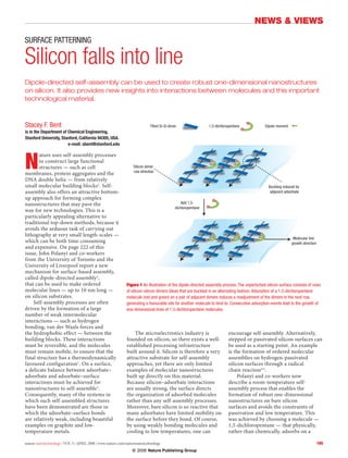
  • 1. NEWS & VIEWS nature nanotechnology | VOL 3 | APRIL 2008 | www.nature.com/naturenanotechnology 185 Stacey F. Bent is in the Department of Chemical Engineering, Stanford University, Stanford, California 94305, USA. e-mail: sbent@stanford.edu N ature uses self-assembly processes to construct large functional structures — such as cell membranes, protein aggregates and the DNA double helix — from relatively small molecular building blocks1 . Self- assembly also offers an attractive bottom- up approach for forming complex nanostructures that may pave the way for new technologies. This is a particularly appealing alternative to traditional top-down methods, because it avoids the arduous task of carrying out lithography at very small length-scales — which can be both time-consuming and expensive. On page 222 of this issue, John Polanyi and co-workers from the University of Toronto and the University of Liverpool report a new mechanism for surface-based assembly, called dipole-directed assembly2 , that can be used to make ordered molecular lines — up to 10 nm long — on silicon substrates. Self-assembly processes are often driven by the formation of a large number of weak intermolecular interactions — such as hydrogen bonding, van der Waals forces and the hydrophobic effect — between the building blocks. These interactions must be reversible, and the molecules must remain mobile, to ensure that the final structure has a thermodynamically favoured configuration1 . On a surface, a delicate balance between adsorbate– adsorbate and adsorbate–surface interactions must be achieved for nanostructures to self-assemble3 . Consequently, many of the systems in which such self-assembled structures have been demonstrated are those in which the adsorbate–surface bonds are relatively weak, including beautiful examples on graphite and low- temperature metals. The microelectronics industry is founded on silicon, so there exists a well- established processing infrastructure built around it. Silicon is therefore a very attractive substrate for self-assembly approaches, yet there are only limited examples of molecular nanostructures built up directly on this material. Because silicon–adsorbate interactions are usually strong, the surface directs the organization of adsorbed molecules rather than any self-assembly processes. Moreover, bare silicon is so reactive that many adsorbates have limited mobility on the surface before they bond. Of course, by using weakly bonding molecules and cooling to low temperatures, one can encourage self-assembly. Alternatively, stepped or passivated silicon surfaces can be used as a starting point. An example is the formation of ordered molecular assemblies on hydrogen-passivated silicon surfaces through a radical chain reaction4,5 . Polanyi and co-workers now describe a room-temperature self- assembly process that enables the formation of robust one-dimensional nanostructures on bare silicon surfaces and avoids the constraints of passivation and low temperature. This was achieved by choosing a molecule — 1,5-dichloropentane — that physically, rather than chemically, adsorbs on a Dipole-directed self-assembly can be used to create robust one-dimensional nanostructures on silicon. It also provides new insights into interactions between molecules and this important technological material. Surface patterning Silicon falls into line Silicon dimer row direction Add 1,5- dichloropentane Molecular line growth direction Buckling induced by adjacent adsorbate Tilted Si-Si dimer 1,5-dichloropentane Dipole moment Figure 1 An illustration of the dipole-directed assembly process. The unperturbed silicon surface consists of rows of silicon–silicon dimers (blue) that are buckled in an alternating fashion. Adsorption of a 1,5-dichloropentane molecule (red and green) on a pair of adjacent dimers induces a readjustment of the dimers in the next row, generating a favourable site for another molecule to bind to. Consecutive adsorption events lead to the growth of one-dimensional lines of 1,5-dichloropentane molecules. © 2008 Nature Publishing Group
  • 2. NEWS VIEWS 186 nature nanotechnology | VOL 3 | APRIL 2008 | www.nature.com/naturenanotechnology silicon substrate at room temperature and does not, therefore, form covalent bonds with the surface that would cause the molecule to break apart. Importantly, this molecule was also chosen because it has a large electric dipole moment — owing to the chlorine atoms at each end of the hydrocarbon chain — and a length that is close to the Si–Si dimer spacing on the Si(100)-(2 × 1) surface. The 1,5-dichloropentane molecules bond to the surface by bridging across two dimers in the same row; both chlorine atoms interact with adjacent silicon atoms. Single 1,5-dichloropentane adsorbates were not observed on the surface, however, suggesting that the individual molecules that did not form part of a larger self-assembled structure were weakly bound and highly mobile. Rather, the molecule assembled into one-dimensional molecular lines that grew orthogonally to the silicon dimer rows (Fig. 1). Interestingly, the direction of line growth was always in the direction opposite to the dipole moment. Theoretical calculations suggested that the energetic driving force for assembly comes from a dipole- induced charge readjustment at the surface. This charge-transfer process causes the adjacent silicon dimers in the next row to buckle in a way that provides a favourable binding site — relative to unaffected dimers — for another 1,5-dichloropentane molecule to adsorb. This effect is the origin of the dipole- directed assembly. An interesting element of this study is that the molecular assembly process involves an interplay between the adsorbate dipole moment and the electronic properties of the surface, leading to self-assembled structures with features influenced by the underlying lattice. The study builds on earlier work that explored the role of surface-charge distribution on molecular bonding to silicon. Theoretical calculations have shown that donation of electronic charge from a nucleophile bonded to the surface spreads to adjacent surface dimers6–8 , and experiments have confirmed that this charge delocalization can be harnessed to direct the assembly of adsorbates6–9 . However, the present study is unusual in that the directed assembly spans across silicon rows, as opposed to the along- row assembly examined in the earlier studies. Moreover, the present study seems to be the first in which criteria for self-assembly are met sufficiently for molecular lines of significant length (up to 10 nm) to be formed. What are the implications and potential of the method for future nanotechnologies? It may offer a new way to ‘set’ a pattern by self-assembly under reasonable temperatures on the silicon substrates. However, this work is just the first step along the road to any future bottom-up nanofabrication process. Subsequent steps are needed to lock the two-dimensional pattern in and propagate it into something more functional, such as nanowires or other three-dimensional structures. What is more significant, however, is that it provides new insight into molecular bonding on silicon substrates and will inspire further studies to determine whether the dipole-directed assembly process is a general one that applies to other molecules, other surfaces, and more complex systems. Undoubtedly, however, silicon will be put firmly in the spotlight to see whether other self- assembly processes lurk on (or beneath) its surface. References 1. Whitesides, G. M. Grzybowski, B. Science 295, 2418–2421 (2002). 2. Harikumar, K. R. et al. Nature Nanotech. 3, 222–228 (2008). 3. Bent, S. F. ACS Nano 1, 10–12 (2007). 4. Lopinski, G. P., Wayner, D. D. M. Wolkow, R. A. Nature 406, 48–51 (2000). 5. Hossain, M. Z., Kato, H. S. Kawai, M. J. Phys. Chem. B 109, 23129–23133 (2005). 6. Queeney, K. T., Chabal, Y. J. Raghavachari, K. Phys. Rev. Lett. 86, 1046–1049 (2001). 7. Widjaja, Y. Musgrave, C. B. Surf. Sci. 469, 9–20 (2000). 8. Wang, Y. Hwang, G. S. J. Chem. Phys. 122, 164706 (2005). 9. Hossain, M. Z., Yamashita, Y. Mukai, K. Yoshinobu, J. Phys. Rev. B 68, 235322 (2003). FUNDAMENTALPHYSICS A most unusual crystal suspended between two platinum electrodes (Nature Physics 4, 314–318; 2008). A Wigner crystal is more likely to be seen in a semiconducting nanotube with large bandgap, but such nanotubes are also more prone to disorder. To overcome this problem Deshpande and Bockrath grew the nanotubes directly from a catalyst on top of one of the electrodes, and measured their transport properties at room temperature to identify devices suitable for more detailed measurements at low temperature. The charge carriers in the nanotubes were ‘holes’ rather than electrons, but the basic physics In 1934, Eugene Wigner — the theoretical physicist who went on to win the Nobel Prize in 1963 — predicted that electrons would enter a novel crystalline phase at low densities when the effects of long-range Coulomb forces between the electrons overwhelmed their kinetic energy. This phase, now known as a Wigner crystal, has been seen in two-dimensional systems but never in one or three dimensions, usually because defects and impurities get in the way. Now Vikram Deshpande and Marc Bockrath of Caltech have seen a one-dimensional Wigner crystal in a single-walled carbon nanotube was the same. The experiment involved cooling the devices to 1.4 K in an applied magnetic field and measuring the number of holes passing through the nanotubes — which were about 500 nm long — as a gate voltage (horizontal axis in the figure above) and the magnetic field strength (vertical axis) were varied; low currents are shown in blue and high currents in red. The Caltech pair actually observed three distinct regimes (separated by the yellow and red lines) with different magnetic and spin properties within the Wigner crystal as the density of holes was varied. Peter Rodgers © 2008 Nature Publishing Group