SlideShare a Scribd company logo
1 of 7
Download to read offline
Dipole-directed assembly of lines of
1,5-dichloropentane on silicon substrates
by displacement of surface charge
K. R. HARIKUMAR1
, TINGBIN LIM1
, IAIN R McNAB1
, JOHN C. POLANYI1
*, LINDA ZOTTI2
,
SERGE AYISSI2 AND WERNER A. HOFER2
1
Department of Chemistry and Institute of Optical Sciences, University of Toronto, 80 St George Street, Toronto, Ontario M5S 3H6, Canada
2
Surface Science Research Centre, University of Liverpool, Liverpool L69 3BX, UK
*e-mail: jpolanyi@chem.utoronto.ca
Published online: 30 March 2008; doi:10.1038/nnano.2008.65
One-dimensional nanostructures at silicon surfaces have potential applications in nanoscale devices. Here we propose a mechanism
of dipole-directed assembly for the growth of lines of physisorbed dipolar molecules. The adsorbate chosen was a halide,
in preparation for the patterned imprinting of halogen atoms. Using scanning tunnelling microscopy, physisorbed
1,5-dichloropentane on Si(100)-231 was shown to self-assemble at room temperature into molecular lines that grew
predominantly perpendicular to the Si-dimer rows. Line formation was triggered by the displacement of surface charge by
the dipolar adsorbate. Experimental and simulated scanning tunnelling microscopy images were in agreement for a range of
positive and negative bias voltages. The geometry of the physisorbed molecules and nature of their binding were evident from
the scanning tunnelling microscopy images, as interpreted by scanning tunnelling microscopy simulation.
Over the last decade many systems have been identified that yield
self-assembled atomic or molecular lines on semiconductors. All
these nanolines were formed as a result of covalent bonding
within or at the surface. Here we describe a method for
the formation of self-assembled molecular lines at room
temperature on a bare Si(100)-2Â1 surface using the novel
approach of dipole-directed assembly (DDA), shown here
for 1,5-dichloropentane (DCP). The adsorbate DCP was chosen
because the Cl...Cl separation in a favoured configuration is
$4 A˚ , closely matching the 3.8 A˚ Si...Si separation between
adjacent Si-dimer pairs, hence offering the possibility of
physisorption in a bridging configuration, with the Cl atoms
located over adjacent Si atoms. The method has also been applied
in initial studies on 1-chloropentane, 1-fluoropentane and
1-chlorododecane.
Earlier works report the study of bismuth nanolines1–6
and rare-
earth silicide nanowires7–16
on Si(100)-2Â1 using scanning
tunnelling microscopy (STM). These lines, of up to 500 nm in
length, grew perpendicular to the Si-dimer rows. The lines were
formed at high substrate temperatures, $600 8C, by sub-surface
reconstruction induced by covalent bonding. Shorter nanolines
formed on Si(100) from group II, III and IV metals (for example,
Mg, Al and Sn) have also been reported17–23
. Lines of physisorbed
molecules have been self-assembled through intermolecular
hydrogen-bonding on smooth graphite (see, for example, ref. 24)
and metal surfaces (see, for example, ref. 25) but not on Si(100).
Chemical chain reactions have also been used to grow
nanolines26–30
. Growth occurred along26–28
and across29,30
the dimer
rows of H-terminated Si(100), initiated from a dangling-bond
site26–30
. Recently, self-assembled molecular lines were formed on a
bare Si(100)-2Â1 surface perpendicular to the dimer rows31
, using
a surface chain reaction initiated by pyrazine.
The adsorbate of the present work, DCP, has been shown by
ab initio calculation to result in a dipole at the surface and to
induce buckling of the Si-dimer pair of an adjacent row. This
buckling favours the adsorption of a molecule at the buckled site.
The second adsorbate molecule induces a further buckling in the
next Si-dimer row and hence a new site favouring molecular
adsorption, and so on, thereby propagating a line of intact
physisorbed molecules, as observed. The direction of line growth is
invariably opposite to the direction of the dipole. The predominant
unidirectionality of the line growth is not explained ab initio; it is
likely to have its origin in the tendency for the relief of surface
strain to take place linearly along an axis of symmetry32–35
.
According to both theory and our STM experiments, the DCP
molecules physisorbed at room temperature with their terminal Cl
atoms interacting with adjacent Si-dimer atoms to one side of the
same dimer row (that is, asymmetrically). The DCP molecular lines
self-assembled unidirectionally in the direction of their asymmetric
point of attachment, and thus opposed to the direction of the C–Cl
dipoles. The direction of line growth was predominantly
perpendicular to the dimer rows.
Simulations matched the STM images for both empty- and
filled-state (positive and negative surface bias) images.
Comparison of the STM images with the simulations yielded the
adsorption geometry of the molecules and therefore the origin of
the likely physisorptive interactions, C–Cl...Si, binding the DCP
to Si atoms at the underlying surface.
A recent theoretical study36,37 of the interactions of dipolar
molecules with Si(100)-2Â1 at high coverages of 0.5 and
ARTICLES
nature nanotechnology | VOL 3 | APRIL 2008 | www.nature.com/naturenanotechnology222
© 2008 Nature Publishing Group
1.0 monolayers predicted four types of important surface effects
resulting in a preference for molecular absorbtion on
neighbouring Si dimers of the row. However, these workers
discounted the possibility of interaction between adjacent dimer
rows, which is central to the present work.
RESULTS AND DISCUSSION
Figure 1a shows an STM image of Si(100)-2Â1 exposed to 1 L
(uncorrected; see Methods for definition of units Langmuir) of
1,5-DCP at room temperature. Intact molecules physisorbed onto
the Si surface and self-assembled to form lines predominantly
perpendicular to the dimer rows. Approximately 5% of the lines
grew diagonally.
The molecule–molecule separation distance was 7.7 A˚ , in
agreement with the long axis of the Si(100)-2Â1 unit cell. The
nanolines consisted of 4–6 molecules on average, 40–50 A˚ long
and 4 A˚ wide. Lines were, however, observed with up to 12
molecules (90–100 A˚ long). Increased line length required low
dose rates (see later). The STM images suggest that the
individual DCP molecules changed their C–Cl bond direction
under the influence of the surface to align their Cl atoms with
two Si-dimer atoms, one from each adjacent dimer pair to one
side of a dimer row, as shown in Fig. 1b. The width of the DCP
lines is comparable with the dimer–dimer distance along a row,
that is, 3.8 A˚ . This structure was confirmed by the ab initio
calculations presented below.
The bright features characteristic of the physisorbed molecules
did not bridge the dimer rows (Fig. 1c,d). This is in contrast to
the molecular lines formed by pyrazine on bare Si(100)-2Â1
midway between two dimer rows, because the pyrazine adsorbate
was bound covalently to the adjacent rows31. The DCP lines
have an experimental height of 0.7 A˚ for 23 V (Fig. 1f). This
agrees with the simulation, which suggests protrusions of $0.8 A˚
in the density contour for this voltage.
The DCP molecules involved in DDA physisorbed and self-
assembled intact. The evidence for physisorption of intact DCP
was that the molecular lines desorbed at elevated temperature
(.$ 200 8C), leaving no residue at the surface. In contrast, a
covalently bound Si–Cl bond formed by reaction at the surface
Diagonal lines
–3.0 V
Distance (Å)
Height(Å)
B
B
A
A
1.8
1.6
1.4
1.2
4 8 12 16
0.7 Å
–3.0 V –3.0 V
Top view
Line
Side view
1,5-DCP
4 Å
Figure 1 Self-assembled molecular nanolines at room temperature. a, A room-temperature STM image (270 Â 270 A˚ ) of a Si(100)-2Â1 surface exposed to
1 L nominally (an uncorrected pressure of 5 Â 1029
torr, 200 s) of DCP. Lines of DCP are imaged as bright features mostly perpendicular to the Si-dimer rows, but
with $5% at 26º to the dimer rows (example circled). The direction of line growth is known, and is shown for several cases by white arrows. Individual DCP features
(bright protrusions) lie to one side of the dimer rows. b, Perspective and top views (left inset). Black dashed lines denote the centre of the Si-dimer rows throughout,
blue spheres denote Cl atoms and blue dotted lines the physisorption interaction. The black arrows indicate the adsorbate dipoles and the long red arrow points in
the direction of line growth. A model of 1,5-DCP is shown in the right inset. c, Close-up (60 Â 40 A˚ ) of the nanoline taken from the white rectangle in a. d, Same
view as in panel c. Red and black ellipses denote dimers and defects, respectively, black-dashed and grey lines indicate the centre of the ridges and the valleys of
the dimer rows. From this picture it is evident that the molecular features (bright protrusions) lie to one side of the dimer rows (to the right as we have oriented
panels c–e). A height profile taken along the blue line in the STM image e is shown in f. The point ‘A’ in the linescan denotes a Si dimer, and the highest point in
profile ‘B’ corresponds to the midpoint of the molecular feature in this line. At this bias (23 V), the average height of the molecular feature with respect to the Si
dimer is 0.7 A˚ . The dark features in the STM images are due mainly to missing-dimer defects.
ARTICLES
nature nanotechnology | VOL 3 | APRIL 2008 | www.nature.com/naturenanotechnology 223
© 2008 Nature Publishing Group
will desorb only above 500 8C (refs 38, 39, 40). Further, DCP
molecular lines were thermally stable up to $200 8C. Above
200 8C, over time, a fraction underwent reaction, severing a
C–Cl bond to give Cl–Si at the surface, characterized by circular
bright spots in the STM image. The bright spots were the Si
dangling bonds adjacent to a reacted Cl (Cl–Si). The remainder
of the DCP adsorbate desorbed from the surface at 200 8C
without chemical reaction, leaving no residue, as expected for a
physisorbed molecule.
As noted, higher dose rates gave shorter lines, and lower dose
rates longer lines; dosing at 1 Â 1029
torr produced lines of 8–10
molecules, whereas 1 Â 1028
torr gave lines of 3–5 molecules.
The STM images indicated that the lines invariably originated in
dimeric DCP, (DCP)2, a characteristic large bright feature evident
at the head of the line in Fig. 2. At the highest dose rate only this
bright feature was observed.
Previously, we found that chloroalkanes on Si(111)-7Â7
predominantly formed dimers at high dose rates, physisorbing
horizontally on Si(111)-7Â7 and Si(100)-2Â1 in contact with
the surface41
. This geometry gave additional binding from the
contact of CH2 with the underlying Si surface, rendering the
horizontal molecules more stable in their adsorbed state42–44
. On
heating, the dimeric (DCP)2 was found, as expected from its
multiple points of attachment, to be more strongly bound to the
surface than the monomer.
In the present experiment, line length was limited by a kinetic
competition between dimer formation (the start of a new line) and
attachment of a monomer to an existing line (resulting in line
growth). Because of the quadratic dependence on monomer
concentration for dimer formation45
, high dose rates favoured the
formation of many dimers, and hence shorter lines.
At room temperature, we observed no features that could be
ascribed to single monomeric DCP molecules in the adsorbed
state, due, presumably, to their high mobility. The observed
molecular lines originated in a stable (DCP)2 dimer—the ‘anchor’
for that line. The lines propagated through linear self-assembly of
a succession of DCP monomers, which, although unstable
individually, were highly stable when self-assembled, even at
elevated temperatures up to $200 8C. At high resolution the lines
in the room-temperature images gave evidence of terminating in
a raised surface feature (Fig. 2), in agreement with expectations
from the DDA model, presented in the following sections.
In other experiments DCP was dosed at a 100 8C Si(100)-2Â1
surface using the same dose rate as in the room-temperature
experiments. No nanolines were observed. Instead, reaction took
place to yield exclusively halogen atoms. Once again, the
remainder of the DCP molecule desorbed. Dosing at 100 8C gave
a smaller coverage, in this case of Cl–Si, by a factor of between
10 and 12, than an equivalent dose at room temperature,
indicating that the sticking probability was lower by this amount
as compared with that at room temperature.
In Fig. 2a we show a high-resolution image of a single DCP line.
The anchor, the DCP dimer (DCP)2, is clearly visible, as are the
individual DCP molecules in the line, and also the Si surface
dimers and back bonds. The end of the line shows a severe
perturbation of the Si dimers. Theory suggests that this
perturbation is due to buckling of the surface originating in the
dipole of the adsorbate (hence ‘dipole-directed assembly’)
encouraging the adsorbtion of a further DCP molecule and
so continuing line growth. Line growth is limited here by
DCP coverage.
Figure 2c to f shows STM images of another DCP line, obtained
with different negative and positive sample biases (left and right,
respectively). The appearance of the line can be seen to be highly
voltage-dependent. The corresponding left and right images were
taken simultaneously with opposite biases in alternate line scans.
In the filled state (negative surface bias, Fig. 2d and f), as the
magnitude of bias was increased the lines brightened. At
sufficiently high negative bias, starting at 22 V (not shown), the
molecular lines were brighter than the Si-dimer rows; at lower
negative biases they appeared darker than the Si-dimer rows. The
+1.0 V
Direction of line growth
B
Xʹ
B
40
X (Å)
Z (Å) 30
20
10
0
1.2
0.8
0.4
0
X
+1.0 V
+0.6 V
+1.5 V –1.5 V
–0.6 V
A
B
Aʹ
Bʹ
A
A
B
B
A
B
Aʹ
Bʹ
Aʹ
Bʹ
Aʹ
Bʹ
DCP2
DCP2DCP2
DCP2
Figure 2 STM images of single nanolines. a, High-resolution image
(50 Â 30 A˚ ) of a single DCP line with a line height profile (inset) taken along the
line X–X0
; the circled feature ‘B’ is the perturbation at the end of the line due to
surface buckling. b, The image of panel a reproduced with ball and stick
molecules superimposed, to scale, of (DCP)2 and DCP over the corresponding
features of the image. c–f, STM images (85 Â 60 A˚ ) of a further single DCP line
at positive and negative voltages; panels c and d were recorded simultaneously
as were panels e and f. An additional DCP dimer (unlabelled) is visible at the
left, adjacent to the line. The white lines A–A0
and B–B0
marked in each image
represent the same features, the ridges of adjacent dimer rows in c–f. In
positive bias the DCP line always appears bright relative to the dimer rows. The
positive-bias images (c and e) show the well-known contrast reversal at and
above þ1.5 V bias; A–A0
and B–B0
then appear as valleys rather than ridges. In
negative-bias images the DCP line appears dark relative to the dimer rows,
brightening as the bias goes to larger negative values. The direction of line
growth is indicated by white arrows; line growth can be seen to begin with a
DCP dimer (DCP)2. Dark trenches are observed to both sides of the DCP lines of
bright molecules; this is due to pinning of adjacent dimers (see text and Fig. 4).
At high bias (positive and negative), the DCP dimers can be seen to be almost
indistinguishable from individual DCP molecules.
ARTICLES
nature nanotechnology | VOL 3 | APRIL 2008 | www.nature.com/naturenanotechnology224
© 2008 Nature Publishing Group
bright features comprising the lines of DCP in the STM images are
calculated to be primarily due to the contribution from the alkyl
chains made visible by the attached halogen atoms46,47
.
Figure 2c,e shows the well-known contrast reversal, in which the
ridge of a dimer row appears bright below 1.5 V and dark above
1.5 V surface bias48–50
.
DENSITY FUNCTIONAL THEORY CALCULATIONS
To understand the formation of molecular lines on the surface we
performed extensive density functional theory (DFT) simulations
(see Methods). In Fig. 3 we show the details of the computed
mechanism for line propagation. Figure 3b shows the state of the
Si dimers p(2Â2) on Si(100), which is in an unperturbed up–
down Si-dimer pair configuration. The up and down Si atoms in
the Si dimers are colour-coded red (up) and dark green (down).
Generally, this configuration corresponds to an excess (up) and a
depletion (down) of electron charge (see, for example, ref. 51).
The two Si-dimer pairs of interest, on which the Cl atoms of the
first DCP will physisorb, are labelled 1B0
and 1C0
. The adsorption
energy using a linear molecule in vacuum as the reference is
2.6 eV per molecule. The energy required to change the C–Cl
bond direction from that in the gas-phase molecule to the
configuration on the surface is approximately 0.2 eV. Calculation
of a DCP dimer clearly showed buckling of the adjacent Si-dimer
pair, as for the DCP monomer. Details of (DCP)2 interaction
with the surface will be published as part of a study of dimeric
adsorbates and their DDA. The present discussion focuses on the
(novel) mechanism of DCP monomer line propagation.
The attachment of a single DCP molecule at 1B0
and 1C0
on row
1 leads to a dipole, both because of a charge transfer from the Cl
atoms of the DCP to adjacent Si dimers and the induced dipole
of the molecule in its adsorbed configuration. This net dipole is
directed perpendicular to the Si-dimer rows with a dipole
strength of 4.85 D (debye) indicated by black arrows in Fig. 3 (we
use the convention that the arrows point from positive to negative
in the dipole). Figure 3c shows buckling of the Si dimers resulting
from the adsorption of this first molecule. The computed charge
redistribution consequent on DCP physisorption is shown in
Fig. 3e; electron density has moved from the Cl atoms (adsorbed
at Si atoms 1B0
and 1C0
) to the other Si atoms of the same dimer
pairs, 1B and 1C, which, consequently, are raised to the ‘up’
configuration (see previous paragraph). Owing to the electrostatic
interaction between the dipole and the Si atoms of the adjacent
row, no. 2 in Fig. 3, dimers 2A, 2A0
; 2B, 2B0
and 2C, 2C0
flip as
shown in Fig. 3c. This may be assisted by the inter-row charge
transfer evident as ‘tails’ in the negative charge gain (G) at the
right of Fig. 3e (ii). The Si-dimer reorientation leads to an energy
gain of 140 meV and provides a preferential adsorption site for
the next molecule in its mobile precursor state.
Supercell
1,5-DCP
Si dimer
Up
1A
1B
1Aʹ
1Bʹ 2B 2Bʹ
2A 2Aʹ 3A
3B
3Aʹ
3Bʹ
1C 1Cʹ 2C 2Cʹ 3C 3Cʹ
1A
1B
1Aʹ
1Bʹ 2B 2Bʹ
2A 2Aʹ 3A
3B
3Aʹ
3Bʹ
1C 1Cʹ
2C 2Cʹ 3C 3Cʹ
1A
1B
1Aʹ
1Bʹ
2B
2Bʹ
2A 2Aʹ 3A
3B
3Aʹ
3Bʹ
1C
1Cʹ
L
i ii
Loss (L) Gain (G)
CI DB
L
1B
1C
G G
G G
2C
2Cʹ
3C 3Cʹ
Down
Figure 3 Mechanism of formation of the molecular line (theory). a,
Schematic representation of the dipoles (short black arrows) responsible for
buckling of the dimers. The locations of the molecules are represented by
golden ellipses. The grey box represents the supercell slab used for the
calculation. The black dashed lines denote the centres of the Si-dimer rows. The
1,5-DCP molecule and the colour-coded ‘up’ and ‘down’ Si dimer atoms are
shown. b, Ground-state Si(100)-p2Â2 surface. The dimer pairs are numbered
1A–1A0
, 1B–1B0
and 1C–1C0
in the left dimer row, 2A–2A0
, 2B–2B0
and
2C–2C0
in the adjacent dimer row and 3A–3A0
, 3B–3B0
and 3C–3C0
in the third
dimer row. The ‘up’ and ‘down’ dimers are colour-coded red and green. c, The
computed buckling due to adsorption of a single molecule on row 1. The bonded
Si atoms 1B0
and 1C0
are down, and 1B and 1C are up. In row 2, 2B0
and 2C0
are up, 2B and 2C are down. The brackets indicate favoured pairs of adsorption
sites for the second DCP molecule. d, Attachment of the second molecule in row
2 repeats for rows 2 and 3 the process of surface-buckling shown for rows 1
and 2 in c. The third adsorbate molecule (not shown) will attach to the
bracketed Si atoms collinear with the first two dipolar adsorbate molecules. e,
Charge redistribution on adsorption of a DCP molecule. (i) Loss (L) in electronic
density within the white contour shown (20.004e A˚ 23
) and (ii) gain (G) in
electronic density within the white contour (þ0.004e A˚ 23
). Colour coding is as
in the other panels. Cl indicates the approximate location of the halogen atom
losing negative charge, and DB the location of the Si dangling bond (1B and 1C)
gaining charge. The black dashed line denotes the centres of the Si dimer rows.
ARTICLES
nature nanotechnology | VOL 3 | APRIL 2008 | www.nature.com/naturenanotechnology 225
© 2008 Nature Publishing Group
The second DCP molecule can only attach at the elevated Si
atoms (2B0
, 2C0
) due to steric hindrance from the first DCP.
Subsequently the pair of Si atoms 2B0
, 2C0
move down (Fig. 3d,
green). This is accompanied by further reorientation at the
adjacent Si-dimer row 3, with elevation of Si atoms 3B0
and 3C0
,
preparing a raised site for attachment of a third DCP (Fig. 3d,
bracketed red atoms). The sequence then continues until the
system either runs out of adsorbate or encounters a defect.
A second DCP molecule migrating across the surface could,
alternatively (Fig. 3c) attach at the pair of Si atoms labelled 2A0
(raised) and 2B0
(raised). A growth direction perpendicular to
the dimer rows is energetically favoured due to dipole
interactions by about 80 meV per molecule relative to diagonal
line growth. The difference in the adsorption energy is sufficient
to make diagonal growth only $5% as likely as perpendicular
growth, at room temperature, as is observed.
In the presence of two adsorbate molecules (Fig. 3d), line
growth in general proceeds collinearly with these molecules; that
is, the lines rarely wander from their initial propagation
direction. A likely explanation is a tendency for strain to relieve
itself linearly in the surface34–37. However, the growth of the line
beyond two DCP molecules is beyond the limit of our supercell,
and hence not calculable.
In summary, adsorbed molecules induce substantial dipoles
(shown as black arrows pointing to the left in Fig. 3), which
result from charge transfer to the surface and the dipole of the
distorted DCP. Electrostatic interactions with this net dipole pin
the Si dimers on the adjacent Si-dimer row, to the right in the
figure, into their new configuration as detailed above, and
propagate the line through self-assembly of additional DCP
monomer molecules away from the direction of the initial
induced dipole. This is the mechanism for DDA.
STM SIMULATIONS
In Fig. 4 we compare the simulated STM image with the
experimental constant-current (0.2 nA) STM images at a sample
bias of +0.6 V. The calculated images reproduce the observation
of a tip–surface distance of 6–7 A˚ . Images were simulated using
a metal tip with a mono-atomic apex at a current of 0.2 nA
(negative bias) and 0.1 nA (positive bias). The current contour in
the positive regime is closer to the surface, so we had to decrease
the contour value to obtain a closed contour surface (see
Methods). Because the 4 Â 4 supercell is too small to describe
the boundary between the molecular lines and the dimer rows,
we used a 4 Â 6 supercell in all simulations. To analyse the effect
of dimer buckling adjacent to the molecular rows we varied the
supercell boundary. The Si dimers have the correct up–down
orientation on one side (above, in the simulations of Fig. 4), but
are flipped in the opposite direction on the other side (below, in
the simulations of Fig. 4). At higher negative bias voltages
(images not shown) we find that the protrusion due to the
adsorbed molecules had its maximum at the position of the
Cl atoms.
The computed images in Fig. 4d have darkness above
the molecular line (X–X0
) and brightness below (Y–Y0
). The
calculated darkness is due to the Si dimer being buckled in the
opposite sense to the rest of its row, as shown in the blue-
bounded insert. Brightness indicates that the Si dimer is buckled
in the same sense as the rest of its row. Experimentally, in both
positive and negative STM images at low bias (+0.6 V; Fig. 4b,e),
we observed darkness at both sides of the line. It would appear
that the dimers on both sides of the molecular rows are pinned,
and the rest of the rows appear bright due to averaging of dimer
positions at room temperature.
+0.6 V, 0.1 nA
–0.6 V, 0.2 nA –0.6 V, 0.2 nA
+0.6 V, 0.2 nA
X
Y
Xʹ
Yʹ
Theory Experiment Experiment + Theory
Figure 4 Comparison between theoretical and experimental images. a,d, Simulated STM images of DCP molecules arranged in lines on Si(100)-p(2Â2) at þ0.6 V
(a) and 20.6 V (d) bias. Each rectangle in the grid represents a 2 Â 1 unit cell (two of which are highlighted by blue rectangles in d, with up and down Si atoms
coloured red and green); DCP molecules are drawn to scale at the right in the simulated images. The centres of the dimer rows in the simulated images are indicated by
dashed lines (corresponding to the ridges of the dimer rows in the experimental images). In the simulated image of the empty state (a), bright protrusions are visible at
the location of the Cl atoms. b,e, Images recorded at the same bias as the simulations (a,d); the appearance of the lines in the simulated images matches well with the
appearance of the lines in the experimental STM images at the same bias. For the positive-bias image, theoretical simulations were made at half the experimental
current (0.1 nA rather than 0.2 nA) so the features due to DCP appear enlarged relative to the experimental image. c,f, The simulated lines are shown superimposed on
the experimental images. The dark arrows X–X0
and Y–Y0
in d show a line of darkness above the molecular line and a line of brightness below the molecular line (see
text). The filled-state STM image at 20.6 V is shown in e; the lines appear darker at this bias, which matches the simulated image d.
ARTICLES
nature nanotechnology | VOL 3 | APRIL 2008 | www.nature.com/naturenanotechnology226
© 2008 Nature Publishing Group
CONCLUSIONS
We report a novel DDA mechanism for the formation of physisorbed
molecular lines at room temperature on a Si(100)-2Â1 surface, as
observed by STM and modelled by DFT calculation. Self-assembly
resulted in lines of intact 1,5-DCP monomers of up to 12
molecules aligned predominantly perpendicular to the dimer
rows, with a 5% minority at a 268 angle to the rows. Once a pair
of molecules established a line direction, that direction was
generally observed to be maintained invariable for all subsequent
molecules in the line.
The mechanism of line propagation of DCP monomers was
shown by DFT calculation to originate in the dipole of an
adsorbed molecule, molecule 1, attached by its two halogen
atoms to adjacent Si atoms along a dimer row. The dipole-
induced charge transfer in the surface is perpendicular to the
Si-dimer row. This transfer of charge resulted in buckling of
adjacent dimer pairs in row 2, giving rise to an attractive site for
molecule 2. A second DCP monomer was adsorbed adjacent to
the first, further shifting the surface charge, thereby buckling row
3 and capturing a third DCP molecule along the extension of the
line formed by the first two, so propagating the line.
At room temperature, DCP monomers are mobile on
Si(100)-2Â1. Line growth originated in a single dimer of (DCP)2
(the anchor) through subsequent collinear assembly of the mobile
DCP monomers. In the STM images the constituent DCP
molecules of the line were displaced to the same side of successive
Si-dimer rows as the direction of line growth, in agreement with
theory. This direction of line growth by DDA is opposite to the
direction of the individual DCP dipoles. Where line growth was
limited by coverage, surface-buckling could be seen by STM in the
Si-dimer row beyond the final DCP molecule of the line. Line
termination was also observed to occur due to defective assembly,
occasioned by a second dimer or by a surface defect.
A requirement for DDA is that the initial adsorbate molecule
has a preferred adsorbate alignment on the surface and a dipole
moment when adsorbed. The orientation of the adsorbate dipole,
through the mediation of surface charge transfer, is opposite to
the propagation direction of the self-assembled line. Further
requirements are that the substrate be electrically polarizable, and
that subsequent molecules to the first be sufficiently mobile to
self-assemble. Charge transfer in the surface manifests itself, in
the present case, as a buckling of the Si atoms of an adjacent
dimer row of Si(100)-2Â1.
The physisorbed dipolar molecular lines observed in this work
were stable up to temperatures of $200 8C, without desorption or
chemical reaction. The finding that mobile dipolar adsorbates can
self-assemble into such robust lines under the influence of charge
transfer to or from the substrate should be of interest in contexts
ranging from nanoscale electronics to molecular biology.
METHODS
EXPERIMENTAL METHODS
Experiments were carried out at room temperature in ultrahigh vacuum (UHV)
using two STM instruments (RHK400 and Omicron-VT) using phosphorous-
doped (n-type, 0.01–0.02 V.cm, 250+25 mm thick) Si(100) reconstructed to
give Si(100)-2Â1. The adsorbate 1,5-DCP (99.9 % pure, Aldrich) was subjected
to repeated freeze–pump–thaw cycles before being introduced to the UHV
chamber through a leak valve for background dosing. Exposures are reported in
Langmuir (1 L ¼ 1 Â 1026
torr s) measured with an uncorrected ion-gauge
calibrated for N2. The corrected doses would be $10 times lower than the stated
doses52. The STM tips were made by a d.c. electrochemical etch of polycrystalline
tungsten wire in a 2 M NaOH solution.
The scanning tunnelling microscopes were operated in the constant-current
mode. All measurements were made with a tunnelling current of 0.2 nA. Samples
were cleaned in UHV by several cycles of d.c. heating to 1,240 8C for $1 min.
The STM images of the surface cleaned in this way showed a (2 Â 1)
reconstruction and , 0.2% surface defects.
ELECTRONIC STRUCTURE SIMULATIONS
The ground-state electronic structure of one or two molecules on Si(100) was
simulated with the Vienna Ab initio Simulation Package (VASP)53,54 using
ultrasoft pseudopotentials and the PW91 parameterization55
of the exchange-
correlation potential. The Si(100) slab contained eight layers, the bottom layer of
which was passivated with hydrogen. We simulated 4 Â 4 and 4 Â 6 supercells,
retaining the p(2Â2) arrangement of the buckled dimers. The high number of
layers was necessary to represent the high elasticity of the silicon lattice. Owing to
the large number of atoms, we limited the simulations of the relaxed geometry to
one k-point at the centre of the surface brillouin zone. The molecular adsorption
site was determined by placing the bent molecules about 3 A˚´
above the surface
plane, with the molecular backbone parallel to the surface. The molecule, as well
as three surface layers, were then fully relaxed until the forces on individual ions
were less than 0.02 eVA˚´ 21
.
The molecular adsorption sites for one- and two-monomer DCP molecules
in a 4 Â 4 and 4 Â 6 Si(100) supercell were calculated using several supercells:
a single DCP molecule in a 4 Â 4 supercell, two molecules in alignment
perpendicular to the dimer rows, two molecules in diagonal alignment, and the
same three arrangements of molecules in a 4 Â 6 supercell. The alignment of
adsorbate molecular dipoles is shown schematically in Fig. 3a. The grey box
represents the supercell slab used for the calculation (not the surface unit cell).
CALCULATION OF DIPOLES
DFT calculation gives a zero dipole for the symmetric linear DCP molecule in the
gas. The dipoles were calculated for a single molecule on the Si(100)-4Â4
supercell using the dipole corrections implemented in our electronic structure
code. For this simulation we first calculated the electron density of the molecules
in the vacuum, then the density of the clean Si surface and finally the density of the
complete system. Subtracting the density of the components from the density of
the complete system yielded the charge transfer due to adsorption. The position
of the dipole was subsequently placed at the median position between positive
and negative charge accumulation, and the dipole moment was calculated using
dipole corrections in (only) two dimensions along the surface plane. We found a
dipole moment of 4.85 D per molecule perpendicular to the dimer rows.
SIMULATION OF STM IMAGES
The STM images for a current of 200 pA (negative bias) or 100 pA (positive bias)
and a range of bias voltages were simulated using the electronic structure of the
converged system, and the multiple scattering approach implemented in
bSKAN56,57
. To improve the accuracy we used a k-point set of 3 Â 3 special
k-points in the final electronic structure simulations, as also for the STM
simulations. To obtain a closed contour surface in the simulation, the current
value in the positive bias regime had to be reduced.
Received 20 September 2007; accepted 27 February 2008;
published 30 March 2008.
References
1. Naitoh, M., Shimaya, H., Nishigaki, S., Oishi, N. & Shoji, F. Scanning tunneling microscopy
observation of bismuth growth on Si(100) surfaces. Surf. Sci. 377–379, 899–903 (1997).
2. Naitoh, M., Shimaya, H., Nishigaki, S., Oishi, N. & Shoji, F. Scanning tunneling microscopy
observation of Bi-induced surface structures on the Si(100) surface. Surf. Sci. 482–485,
1440–1444 (2001).
3. Owen, J. H. G., Miki, K. & Bowler, D. R. Self-assembled nanowires on semiconductor surfaces.
J. Mater. Sci. 41, 4568–4603 (2006).
4. MacLeod, J. M. & McLean, A. B. Single 2 Â 1 domain orientation on Si(100) surfaces using a
periodic Bi line arrays. Phys. Rev B 70, 041306 (2004).
5. MacLeod, J. M., Miwa, R. H., Srivastava, G. P. & McLean, A. B. The electronic origin of contrast
reversal in bias-dependent STM images of nanolines. Surf. Sci. 576, 116–122 (2005).
6. Preinesberger, C., Vandre, S., Kalka, T. & Dahne-Preitsch, M. Formation of dysprosium silicide wires
on Si(001) . J. Phys. D 31, L43–L45 (1998).
7. Chen, Y., Ohlberg, D. A. A. & Williams, R. S. Nanowires of four epitaxial hexagonal silicides grown
on Si(001). J. Appl. Phys. 91, 3213–3218 (2002).
8. Nogami, J., Liu, B. Z., Katkov, M. V., Ohbuchi, C. & Birge, N. O. Self-assembled rare earth silicide
nanowires on Si(001). Phys. Rev. B 63, 233305 (2001).
9. Liu, B. Z. & Nogami, J. Growth of parallel rare earth silicide nanowire arrays on vicinal Si(001).
Nanotechnology 14, 873–877 (2003).
10. Liu, B. Z. & Nogami, J. An STM study of the Si(001)(2Â4)-Dy surface. Surf. Sci. 488,
399–405 (2001).
11. Ohbuchi, C. & Nogami, J. Holmium growth on Si(001): Surface reconstructions and nanowire
formation. Phys. Rev. B 66, 165323 (2002).
12. Katkov, M. V. & Nogami, J. Yb and Nd growth on Si(001). Surf. Sci. 524, 129–136 (2003).
ARTICLES
nature nanotechnology | VOL 3 | APRIL 2008 | www.nature.com/naturenanotechnology 227
© 2008 Nature Publishing Group
13. Ohbuchi, C. & Nogami, J. Samarium induced surface reconstructions of Si(001). Surf. Sci. 579,
157–165 (2005).
14. Harrison, B. C. & Boland, J. J. Real-time STM study of inter-nanowire reactions: GdSi2 nanowires on
Si(100). Surf. Sci. 594, 93–98 (2005).
15. Evans, M. M. R. & Nogami, J. Indium and gallium on Si(001): A closer look at the parallel dimer
structure . Phys. Rev. B 59, 7644–7648 (1999).
16. Nogami, J., Baski, A. A. & Quate, C. F. Aluminum on the Si(100) surface: Growth of the first
monolayer. Phys. Rev. B 44, 1415–1418 (1991).
17. Glueckstein, J. C., Evans, M. M. R. & Nogami, J. Growth of Sn on Si(001) at room temperature.
Surf. Sci. 415, 80–94 (1998).
18. Itoh, H., Tanabe, H., Winau, D., Schmid, A. K. & Ichinokawa, T. Growth mode and surface structures
of the Pb/Si(001) system observed by scanning tunneling microscopy. J. Vac. Sci. Tech. B 12,
2086–2089 (1994).
19. Tomatsu, K., Nakatsuji, K., Iimori, T. & Komori, F. STM observation of initial growth of Sn atoms on
Ge(001) surface. Surf. Sci. 601, 1736–1746 (2007).
20. Hutchison, P., Evans, M. M. R. & Nogami, J. Mg growth on the Si(001) surface: An STM study.
Surf. Sci. 411, 99–110 (1998).
21. Bakhtizin, R. Z., Kishimoto, J., Hashizume, T. & Sakurai, T. STM study of Sr adsorption on Si(100)
surface. Appl. Surf. Sci. 94, 478–484 (1996).
22. Bird, C. F. & Bowler, D. R. A spin polarized first-principles study of short dangling bond wires on
Si(001). Surf. Sci. 531, L351–L355 (2003).
23. Chen, T. C. et al. Atomic-scale desorption through electronic and vibrational excitation mechanisms.
Science 268, 1590–1592 (1995).
24. Cyr, C. M., Venkataraman, B. & Flynn, G. W. Functional group identification in scanning tunneling
microscopy of molecular adsorbates. J. Phys. Chem. 100, 13747–13759 (1996).
25. Canas-Ventura, M. E. et al. Coexistence of one- and two-dimensional supramolecular assemblies of
terephthalic acid on Pd(111) due to self-limiting deprotonation. J. Chem Phys. 125, 184710 (2006).
26. Lopinski, G. P., Wayner, D. D. M. & Wolkow, R. A. Self-directed growth of molecular nanostructures
on silicon. Nature 406, 48–51 (2000).
27. DiLabio, G. A., Piva, P. G., Kruse, P. & Wolkow, R. A. Dispersion interactions enable the self-directed
growth of linear alkane nanostructures covalently bound to silicon. J. Am. Chem. Soc.
126, 16048–16050 (2004).
28. Kruse, P., Johnson, E. R., DiLabio, G. A. & Wolkow, R. A. Patterning of vinylferrocene on H–Si(100)
via self-directed growth of molecular lines and STM-induced decomposition. Nano Lett. 2,
807–810 (2002).
29. Hossain, M. Z., Kato, H. S. & Kawai, M. Controlled fabrication of 1D molecular lines across the
dimer rows on the Si(100)-(2 Â 1)-H surface through the radical chain reaction. J. Am. Soc. Chem.
127, 15030–15031 (2005).
30. Hossain, M. Z., Kato, H. S. & Kawai, M. Fabrication of interconnected 1D molecular lines along
and across the dimer rows on the Si(100)-(2 Â 1)-H surface through the radical chain reaction.
J. Phys. Chem. B 109, 23129–23133 (2005).
31. Shimomura, M. et al. Formation of one-dimensional molecular chains on a solid surface:
Pyrazine/Si(001). Phys. Rev. B 72, 033303 (2005).
32. Wang, Y., Chen, X. & Hamers, R. J. Atomic-resolution study of overlayer formation and interfacial
mixing in the interaction of phosphorus with Si(001). Phys. Rev. B 50, 4534–4547 (1994).
33. Kipp, L. et al. Adsorption and decomposition on Si(100) 2 Â 1 studied by STM . Phys. Rev. B 52,
5843–5850 (1995).
34. Knall, J. & Pethica, J. B. Growth of Ge on Si(100) and Si(113) studied by STM. Surf. Sci. 265,
156–167 (1992).
35. Park, Ch., Bakhizin, R. Z., Hashizume, T. & Sakurai, T. Strain relief and ordering of (2 Â n)-Bi
structure on Si(100). J. Vac. Sci. Technol. B 12, 2049–2051 (1994).
36. Wang, Y. & Hwang, G. S. Two-dimension arrangement of CH3NH2 adsorption on Si(001)-2Â1.
Chem. Phys. Lett. 385, 144–148 (2004).
37. Wang, Y. & Hwang, G. S. Origin of nonlocal interactions in adsorption of polar molecules on
Si(001)-2Â1. J. Chem. Phys. 122, 164706 (2005).
38. Gao, Q., Cheng, C. C., Chen, P. J., Choyke, W. J. & Yates, J. T. Jr. Chlorine bonding sites and bonding
configurations on Si(100)-2 Â 1. J. Chem. Phys. 98, 8308–8323 (1993).
39. Szabo, A., Farrall, P. D. & Engel, T. Reactions of chlorine with Si(100) and Si(111): Adsorption and
desorption kinetics. Surf. Sci. 312, 284–300 (1994).
40. Gupta, P., Coon, P. A., Koehler, B. G. & George, S. M. Desorption product yields following Cl2
adsorption on Si(111)-7 Â 7: Coverage and temperature dependence. Surf. Sci. 249, 92–104 (1991).
41. Dobrin, S. et al. Self-assembled molecular corrals on a semiconductor surface. Surf. Sci.
600, 43–47 (2006).
42. Dubois, M., Delerue, C. & Rubio, A. Adsorption and electronic excitation of biphenyl on Si(100):
a theoretical STM analysis. Phys. Rev. B 75, 041302 (2004).
43. Grandidier, B. et al. Effect of alkyl substituents on the adsorption of thienylenevinylene oligomers on
the Si(100) surface. Surf. Sci. 473, 1–7 (2001).
44. Lei, R. Z., Gellman, A. J. & Koel, B. E. Desorption energies of linear and cyclic alkanes on surfaces:
Anomalous scaling with length. Surf. Sci. 554, 125–140 (2004).
45. Dobrin, S. et al. Molecular dynamics of haloalkane corral-formation and surface halogenation at
Si(111)-7 Â 7. J. Chem. Phys. 125, 133407 (2006).
46. Grandidier, B. et al. Effect of alkyl substituents on the adsorption of thienylenevinylene oligomers on
the Si(100) surface. Surf. Sci. 473, 1–7 (2001).
47. Dubois, M., Delerue, C. & Allan G. Scanning tunneling microscopy and spectroscopy of conjugated
oligomers weakly bonded to Si(100) surfaces: A theoretical study. Phys. Rev. B 71, 165435 (2005).
48. Kondo, Y., Amakusa, T., Iwatsuki, M. & Tokomoto, H. Phase transition of the Si(001) surface below
100 K. Surf. Sci. 453, L318–L322 (2000).
49. Lyubinetsky, I., Dohnalek, Z., Choyke, W. J. & Yates, J. T. Jr. Cl2 dissociation on Si(100)-(2 Â 1):
A statistical study by scanning tunneling microscopy. Phys. Rev. B 58, 7950–7957 (1998).
50. Okada, H., Fujimoto, Y., Endo, K., Hirose, K. & Mori, Y. Detailed analysis of scanning tunneling
microscopy images of the Si(001) reconstructed surface with buckled dimers. Phys. Rev. B 63,
195324 (2001).
51. Oura, K., Lifshits, V. G., Saranin, A. A., Zotov, A. V. & Katayama, M. Surface Science: An Introduction
181–183 (Springer-Verlag, Berlin, 2003).
52. Bartmess, J. E. & Georgiadis, R. M. Empirical methods for determination of ion gauge sensitivities
for different gases. Vacuum 33, 149–153 (1983).
53. Kresse, G. & Hafner, J. Ab initio molecular dynamics for liquid metals. Phys. Rev. B
47, 558–561 (1993).
54. Kresse, G. & Furthmu¨ller, J. Efficient iterative schemes for ab initio total-energy calculations using a
plane-wave basis set. Phys. Rev. B 54, 11169–11186 (1996).
55. Perdew, J. P. et al. Atoms, molecules, solids, and surfaces: Applications of the generalized gradient
approximation for exchange and correlation. Phys. Rev. B 46, 6671–6687 (1992).
56. Hofer, W. A. & Redinger, J. STM of binary alloys: First principles calculation of the current for
PtX(100) surfaces. Surf. Sci. 447, 51–61 (2000).
57. Palotas, K. & Hofer, W. A. Multiple scattering in a vacuum barrier obtained from real-space
wavefunctions. J. Phys. Condens. Matter 17, 2705–2713 (2005).
Acknowledgements
The authors are indebted to the Natural Sciences and Engineering Research Council of Canada (NSERC),
the Ontario Centers of Excellence (OCE) Centre for Photonics, the Canadian Institute for Photonic
Innovation (CIPI), and the Canadian Institute For Advanced Research (CIFAR) for their support. We
thank L. Leung for helpful discussions. W.A.H. thanks the Royal Society for financial support.
Correspondence and requests for materials should be addressed to J.C.P.
Author contributions
The experiments were performed jointly by K.R.H., T.L., I.R.M. and J.C.P. at the University of Toronto,
and the computations by L.Z., S.A. and W.A.H. at the University of Liverpool.
Reprints and permission information is available online at http://npg.nature.com/reprintsandpermissions/
ARTICLES
nature nanotechnology | VOL 3 | APRIL 2008 | www.nature.com/naturenanotechnology228
© 2008 Nature Publishing Group

More Related Content

What's hot

INORG CHEM Cu-S Ist paper Prashant
INORG CHEM Cu-S Ist paper PrashantINORG CHEM Cu-S Ist paper Prashant
INORG CHEM Cu-S Ist paper PrashantPrashant Sharma
 
Chapter 03 organic compounds alkanes and cycloalkanes
Chapter 03 organic compounds alkanes and cycloalkanesChapter 03 organic compounds alkanes and cycloalkanes
Chapter 03 organic compounds alkanes and cycloalkanesWong Hsiung
 
Chapter 05 stereochemistry at tetrahedral centers
Chapter 05 stereochemistry at tetrahedral centersChapter 05 stereochemistry at tetrahedral centers
Chapter 05 stereochemistry at tetrahedral centersWong Hsiung
 
2010 cu c fiber hybrids carbon 2106
2010 cu c fiber hybrids carbon 21062010 cu c fiber hybrids carbon 2106
2010 cu c fiber hybrids carbon 2106Nourre
 
Chapter 2 polar covalent bonds acids and bases
Chapter 2 polar covalent bonds acids and basesChapter 2 polar covalent bonds acids and bases
Chapter 2 polar covalent bonds acids and basesWong Hsiung
 
Size control of Nanoparticles
Size control of NanoparticlesSize control of Nanoparticles
Size control of NanoparticlesOscar1Miranda2
 
Conformation and configuration sujith
Conformation and configuration   sujithConformation and configuration   sujith
Conformation and configuration sujithSUJITH KP
 
Stereochemistry of Alkanes and Cycloalkanes
Stereochemistry of Alkanes and CycloalkanesStereochemistry of Alkanes and Cycloalkanes
Stereochemistry of Alkanes and CycloalkanesNilesh Thakare
 

What's hot (11)

INORG CHEM Cu-S Ist paper Prashant
INORG CHEM Cu-S Ist paper PrashantINORG CHEM Cu-S Ist paper Prashant
INORG CHEM Cu-S Ist paper Prashant
 
Stereochemistry
StereochemistryStereochemistry
Stereochemistry
 
Ch03.alkanes
Ch03.alkanesCh03.alkanes
Ch03.alkanes
 
Chapter 03 organic compounds alkanes and cycloalkanes
Chapter 03 organic compounds alkanes and cycloalkanesChapter 03 organic compounds alkanes and cycloalkanes
Chapter 03 organic compounds alkanes and cycloalkanes
 
Chapter 05 stereochemistry at tetrahedral centers
Chapter 05 stereochemistry at tetrahedral centersChapter 05 stereochemistry at tetrahedral centers
Chapter 05 stereochemistry at tetrahedral centers
 
2010 cu c fiber hybrids carbon 2106
2010 cu c fiber hybrids carbon 21062010 cu c fiber hybrids carbon 2106
2010 cu c fiber hybrids carbon 2106
 
Chapter 2 polar covalent bonds acids and bases
Chapter 2 polar covalent bonds acids and basesChapter 2 polar covalent bonds acids and bases
Chapter 2 polar covalent bonds acids and bases
 
Size control of Nanoparticles
Size control of NanoparticlesSize control of Nanoparticles
Size control of Nanoparticles
 
Conformation and configuration sujith
Conformation and configuration   sujithConformation and configuration   sujith
Conformation and configuration sujith
 
Stereochemistry of Alkanes and Cycloalkanes
Stereochemistry of Alkanes and CycloalkanesStereochemistry of Alkanes and Cycloalkanes
Stereochemistry of Alkanes and Cycloalkanes
 
Ch5
Ch5Ch5
Ch5
 

Similar to Dipole-directed Assembly of Lines of Dichloropentane on Silicon Substrates by Displacement of Surface Charge

1997 nucleation of homoepitaxial si chains on si(001) at room temperature
1997 nucleation of homoepitaxial si chains on si(001) at room temperature1997 nucleation of homoepitaxial si chains on si(001) at room temperature
1997 nucleation of homoepitaxial si chains on si(001) at room temperaturepmloscholte
 
A molecular-dynamics-simulation-of-the-structure-and-properties-of-a-self-ass...
A molecular-dynamics-simulation-of-the-structure-and-properties-of-a-self-ass...A molecular-dynamics-simulation-of-the-structure-and-properties-of-a-self-ass...
A molecular-dynamics-simulation-of-the-structure-and-properties-of-a-self-ass...Darren Martin Leith
 
1998 epitaxial film growth of the charge density-wave conductor rb0.30 moo3 o...
1998 epitaxial film growth of the charge density-wave conductor rb0.30 moo3 o...1998 epitaxial film growth of the charge density-wave conductor rb0.30 moo3 o...
1998 epitaxial film growth of the charge density-wave conductor rb0.30 moo3 o...pmloscholte
 
Molecular dynamics-of-ions-in-two-forms-of-an-electroactive-polymer
Molecular dynamics-of-ions-in-two-forms-of-an-electroactive-polymerMolecular dynamics-of-ions-in-two-forms-of-an-electroactive-polymer
Molecular dynamics-of-ions-in-two-forms-of-an-electroactive-polymerDarren Martin Leith
 
Origami conductivity and structural stability
Origami conductivity and structural stabilityOrigami conductivity and structural stability
Origami conductivity and structural stabilitydodo5575
 
Characterization of expanded austenite in stainless steels by ion carburizati...
Characterization of expanded austenite in stainless steels by ion carburizati...Characterization of expanded austenite in stainless steels by ion carburizati...
Characterization of expanded austenite in stainless steels by ion carburizati...Javier García Molleja
 
Self-Assembled Molecular Corrals on a Semiconductor Surface
Self-Assembled Molecular Corrals on a Semiconductor SurfaceSelf-Assembled Molecular Corrals on a Semiconductor Surface
Self-Assembled Molecular Corrals on a Semiconductor Surfaceioneec
 
1997 sodium doped dimer rows on si(001)
1997 sodium doped dimer rows on si(001)1997 sodium doped dimer rows on si(001)
1997 sodium doped dimer rows on si(001)pmloscholte
 
4.2.cappelli 06(3)
4.2.cappelli 06(3)4.2.cappelli 06(3)
4.2.cappelli 06(3)ELIMENG
 
4.2.cappelli 06(2)
4.2.cappelli 06(2)4.2.cappelli 06(2)
4.2.cappelli 06(2)ELIMENG
 
4.2.cappelli 06(1)
4.2.cappelli 06(1)4.2.cappelli 06(1)
4.2.cappelli 06(1)ELIMENG
 
4.2.cappelli 06
4.2.cappelli 064.2.cappelli 06
4.2.cappelli 06ELIMENG
 
Temperature Dependence of the Band-Edge Transitions of ZnCdBeSe
Temperature Dependence of the Band-Edge Transitions of ZnCdBeSeTemperature Dependence of the Band-Edge Transitions of ZnCdBeSe
Temperature Dependence of the Band-Edge Transitions of ZnCdBeSeOleg Maksimov
 
michele_romeo_phd_final_exam_presentation
michele_romeo_phd_final_exam_presentationmichele_romeo_phd_final_exam_presentation
michele_romeo_phd_final_exam_presentationMichele Romeo
 
XRD principle and application
XRD principle and applicationXRD principle and application
XRD principle and applicationTechef In
 
Report_Paulo_Melo_LabI
Report_Paulo_Melo_LabIReport_Paulo_Melo_LabI
Report_Paulo_Melo_LabIPaulo Melo
 

Similar to Dipole-directed Assembly of Lines of Dichloropentane on Silicon Substrates by Displacement of Surface Charge (20)

1997 nucleation of homoepitaxial si chains on si(001) at room temperature
1997 nucleation of homoepitaxial si chains on si(001) at room temperature1997 nucleation of homoepitaxial si chains on si(001) at room temperature
1997 nucleation of homoepitaxial si chains on si(001) at room temperature
 
1601.02214
1601.022141601.02214
1601.02214
 
A molecular-dynamics-simulation-of-the-structure-and-properties-of-a-self-ass...
A molecular-dynamics-simulation-of-the-structure-and-properties-of-a-self-ass...A molecular-dynamics-simulation-of-the-structure-and-properties-of-a-self-ass...
A molecular-dynamics-simulation-of-the-structure-and-properties-of-a-self-ass...
 
1998 epitaxial film growth of the charge density-wave conductor rb0.30 moo3 o...
1998 epitaxial film growth of the charge density-wave conductor rb0.30 moo3 o...1998 epitaxial film growth of the charge density-wave conductor rb0.30 moo3 o...
1998 epitaxial film growth of the charge density-wave conductor rb0.30 moo3 o...
 
Molecular dynamics-of-ions-in-two-forms-of-an-electroactive-polymer
Molecular dynamics-of-ions-in-two-forms-of-an-electroactive-polymerMolecular dynamics-of-ions-in-two-forms-of-an-electroactive-polymer
Molecular dynamics-of-ions-in-two-forms-of-an-electroactive-polymer
 
Adv Mat 2015
Adv Mat 2015Adv Mat 2015
Adv Mat 2015
 
IITJEE - Physics 2011-i
IITJEE - Physics   2011-iIITJEE - Physics   2011-i
IITJEE - Physics 2011-i
 
Origami conductivity and structural stability
Origami conductivity and structural stabilityOrigami conductivity and structural stability
Origami conductivity and structural stability
 
Characterization of expanded austenite in stainless steels by ion carburizati...
Characterization of expanded austenite in stainless steels by ion carburizati...Characterization of expanded austenite in stainless steels by ion carburizati...
Characterization of expanded austenite in stainless steels by ion carburizati...
 
Self-Assembled Molecular Corrals on a Semiconductor Surface
Self-Assembled Molecular Corrals on a Semiconductor SurfaceSelf-Assembled Molecular Corrals on a Semiconductor Surface
Self-Assembled Molecular Corrals on a Semiconductor Surface
 
Ijetr021521
Ijetr021521Ijetr021521
Ijetr021521
 
1997 sodium doped dimer rows on si(001)
1997 sodium doped dimer rows on si(001)1997 sodium doped dimer rows on si(001)
1997 sodium doped dimer rows on si(001)
 
4.2.cappelli 06(3)
4.2.cappelli 06(3)4.2.cappelli 06(3)
4.2.cappelli 06(3)
 
4.2.cappelli 06(2)
4.2.cappelli 06(2)4.2.cappelli 06(2)
4.2.cappelli 06(2)
 
4.2.cappelli 06(1)
4.2.cappelli 06(1)4.2.cappelli 06(1)
4.2.cappelli 06(1)
 
4.2.cappelli 06
4.2.cappelli 064.2.cappelli 06
4.2.cappelli 06
 
Temperature Dependence of the Band-Edge Transitions of ZnCdBeSe
Temperature Dependence of the Band-Edge Transitions of ZnCdBeSeTemperature Dependence of the Band-Edge Transitions of ZnCdBeSe
Temperature Dependence of the Band-Edge Transitions of ZnCdBeSe
 
michele_romeo_phd_final_exam_presentation
michele_romeo_phd_final_exam_presentationmichele_romeo_phd_final_exam_presentation
michele_romeo_phd_final_exam_presentation
 
XRD principle and application
XRD principle and applicationXRD principle and application
XRD principle and application
 
Report_Paulo_Melo_LabI
Report_Paulo_Melo_LabIReport_Paulo_Melo_LabI
Report_Paulo_Melo_LabI
 

More from ioneec

IONEEC - How To Stimulate Your Art?
IONEEC - How To Stimulate Your Art?IONEEC - How To Stimulate Your Art?
IONEEC - How To Stimulate Your Art?ioneec
 
Monte Carlo Simulation Methods
Monte Carlo Simulation MethodsMonte Carlo Simulation Methods
Monte Carlo Simulation Methodsioneec
 
Iron Doped Titania Nanostructures Synthesis, DFT modelling and Photocatalysis
Iron Doped Titania Nanostructures Synthesis, DFT modelling and PhotocatalysisIron Doped Titania Nanostructures Synthesis, DFT modelling and Photocatalysis
Iron Doped Titania Nanostructures Synthesis, DFT modelling and Photocatalysisioneec
 
Silicon Falls Into Line
Silicon Falls Into LineSilicon Falls Into Line
Silicon Falls Into Lineioneec
 
Maskless Nanopattering and Formation of Nanocorrals and Switches for Haloalka...
Maskless Nanopattering and Formation of Nanocorrals and Switches for Haloalka...Maskless Nanopattering and Formation of Nanocorrals and Switches for Haloalka...
Maskless Nanopattering and Formation of Nanocorrals and Switches for Haloalka...ioneec
 
Electronic Switching of Single Silicon Atoms by Molecular Field Effects
Electronic Switching of Single Silicon Atoms by Molecular Field EffectsElectronic Switching of Single Silicon Atoms by Molecular Field Effects
Electronic Switching of Single Silicon Atoms by Molecular Field Effectsioneec
 
5 Reasons to use IONEEC
5 Reasons to use IONEEC5 Reasons to use IONEEC
5 Reasons to use IONEECioneec
 
Last jp403835m
Last jp403835mLast jp403835m
Last jp403835mioneec
 
Acs ejpcc-e5b01406
Acs ejpcc-e5b01406Acs ejpcc-e5b01406
Acs ejpcc-e5b01406ioneec
 

More from ioneec (9)

IONEEC - How To Stimulate Your Art?
IONEEC - How To Stimulate Your Art?IONEEC - How To Stimulate Your Art?
IONEEC - How To Stimulate Your Art?
 
Monte Carlo Simulation Methods
Monte Carlo Simulation MethodsMonte Carlo Simulation Methods
Monte Carlo Simulation Methods
 
Iron Doped Titania Nanostructures Synthesis, DFT modelling and Photocatalysis
Iron Doped Titania Nanostructures Synthesis, DFT modelling and PhotocatalysisIron Doped Titania Nanostructures Synthesis, DFT modelling and Photocatalysis
Iron Doped Titania Nanostructures Synthesis, DFT modelling and Photocatalysis
 
Silicon Falls Into Line
Silicon Falls Into LineSilicon Falls Into Line
Silicon Falls Into Line
 
Maskless Nanopattering and Formation of Nanocorrals and Switches for Haloalka...
Maskless Nanopattering and Formation of Nanocorrals and Switches for Haloalka...Maskless Nanopattering and Formation of Nanocorrals and Switches for Haloalka...
Maskless Nanopattering and Formation of Nanocorrals and Switches for Haloalka...
 
Electronic Switching of Single Silicon Atoms by Molecular Field Effects
Electronic Switching of Single Silicon Atoms by Molecular Field EffectsElectronic Switching of Single Silicon Atoms by Molecular Field Effects
Electronic Switching of Single Silicon Atoms by Molecular Field Effects
 
5 Reasons to use IONEEC
5 Reasons to use IONEEC5 Reasons to use IONEEC
5 Reasons to use IONEEC
 
Last jp403835m
Last jp403835mLast jp403835m
Last jp403835m
 
Acs ejpcc-e5b01406
Acs ejpcc-e5b01406Acs ejpcc-e5b01406
Acs ejpcc-e5b01406
 

Recently uploaded

SOLUBLE PATTERN RECOGNITION RECEPTORS.pptx
SOLUBLE PATTERN RECOGNITION RECEPTORS.pptxSOLUBLE PATTERN RECOGNITION RECEPTORS.pptx
SOLUBLE PATTERN RECOGNITION RECEPTORS.pptxkessiyaTpeter
 
Animal Communication- Auditory and Visual.pptx
Animal Communication- Auditory and Visual.pptxAnimal Communication- Auditory and Visual.pptx
Animal Communication- Auditory and Visual.pptxUmerFayaz5
 
Unlocking the Potential: Deep dive into ocean of Ceramic Magnets.pptx
Unlocking  the Potential: Deep dive into ocean of Ceramic Magnets.pptxUnlocking  the Potential: Deep dive into ocean of Ceramic Magnets.pptx
Unlocking the Potential: Deep dive into ocean of Ceramic Magnets.pptxanandsmhk
 
Formation of low mass protostars and their circumstellar disks
Formation of low mass protostars and their circumstellar disksFormation of low mass protostars and their circumstellar disks
Formation of low mass protostars and their circumstellar disksSérgio Sacani
 
Artificial Intelligence In Microbiology by Dr. Prince C P
Artificial Intelligence In Microbiology by Dr. Prince C PArtificial Intelligence In Microbiology by Dr. Prince C P
Artificial Intelligence In Microbiology by Dr. Prince C PPRINCE C P
 
Boyles law module in the grade 10 science
Boyles law module in the grade 10 scienceBoyles law module in the grade 10 science
Boyles law module in the grade 10 sciencefloriejanemacaya1
 
Biopesticide (2).pptx .This slides helps to know the different types of biop...
Biopesticide (2).pptx  .This slides helps to know the different types of biop...Biopesticide (2).pptx  .This slides helps to know the different types of biop...
Biopesticide (2).pptx .This slides helps to know the different types of biop...RohitNehra6
 
All-domain Anomaly Resolution Office U.S. Department of Defense (U) Case: “Eg...
All-domain Anomaly Resolution Office U.S. Department of Defense (U) Case: “Eg...All-domain Anomaly Resolution Office U.S. Department of Defense (U) Case: “Eg...
All-domain Anomaly Resolution Office U.S. Department of Defense (U) Case: “Eg...Sérgio Sacani
 
CALL ON ➥8923113531 🔝Call Girls Kesar Bagh Lucknow best Night Fun service 🪡
CALL ON ➥8923113531 🔝Call Girls Kesar Bagh Lucknow best Night Fun service  🪡CALL ON ➥8923113531 🔝Call Girls Kesar Bagh Lucknow best Night Fun service  🪡
CALL ON ➥8923113531 🔝Call Girls Kesar Bagh Lucknow best Night Fun service 🪡anilsa9823
 
Presentation Vikram Lander by Vedansh Gupta.pptx
Presentation Vikram Lander by Vedansh Gupta.pptxPresentation Vikram Lander by Vedansh Gupta.pptx
Presentation Vikram Lander by Vedansh Gupta.pptxgindu3009
 
G9 Science Q4- Week 1-2 Projectile Motion.ppt
G9 Science Q4- Week 1-2 Projectile Motion.pptG9 Science Q4- Week 1-2 Projectile Motion.ppt
G9 Science Q4- Week 1-2 Projectile Motion.pptMAESTRELLAMesa2
 
Work, Energy and Power for class 10 ICSE Physics
Work, Energy and Power for class 10 ICSE PhysicsWork, Energy and Power for class 10 ICSE Physics
Work, Energy and Power for class 10 ICSE Physicsvishikhakeshava1
 
PossibleEoarcheanRecordsoftheGeomagneticFieldPreservedintheIsuaSupracrustalBe...
PossibleEoarcheanRecordsoftheGeomagneticFieldPreservedintheIsuaSupracrustalBe...PossibleEoarcheanRecordsoftheGeomagneticFieldPreservedintheIsuaSupracrustalBe...
PossibleEoarcheanRecordsoftheGeomagneticFieldPreservedintheIsuaSupracrustalBe...Sérgio Sacani
 
Call Girls in Mayapuri Delhi 💯Call Us 🔝9953322196🔝 💯Escort.
Call Girls in Mayapuri Delhi 💯Call Us 🔝9953322196🔝 💯Escort.Call Girls in Mayapuri Delhi 💯Call Us 🔝9953322196🔝 💯Escort.
Call Girls in Mayapuri Delhi 💯Call Us 🔝9953322196🔝 💯Escort.aasikanpl
 
Biological Classification BioHack (3).pdf
Biological Classification BioHack (3).pdfBiological Classification BioHack (3).pdf
Biological Classification BioHack (3).pdfmuntazimhurra
 
Natural Polymer Based Nanomaterials
Natural Polymer Based NanomaterialsNatural Polymer Based Nanomaterials
Natural Polymer Based NanomaterialsAArockiyaNisha
 
Labelling Requirements and Label Claims for Dietary Supplements and Recommend...
Labelling Requirements and Label Claims for Dietary Supplements and Recommend...Labelling Requirements and Label Claims for Dietary Supplements and Recommend...
Labelling Requirements and Label Claims for Dietary Supplements and Recommend...Lokesh Kothari
 
Discovery of an Accretion Streamer and a Slow Wide-angle Outflow around FUOri...
Discovery of an Accretion Streamer and a Slow Wide-angle Outflow around FUOri...Discovery of an Accretion Streamer and a Slow Wide-angle Outflow around FUOri...
Discovery of an Accretion Streamer and a Slow Wide-angle Outflow around FUOri...Sérgio Sacani
 
Spermiogenesis or Spermateleosis or metamorphosis of spermatid
Spermiogenesis or Spermateleosis or metamorphosis of spermatidSpermiogenesis or Spermateleosis or metamorphosis of spermatid
Spermiogenesis or Spermateleosis or metamorphosis of spermatidSarthak Sekhar Mondal
 
Hubble Asteroid Hunter III. Physical properties of newly found asteroids
Hubble Asteroid Hunter III. Physical properties of newly found asteroidsHubble Asteroid Hunter III. Physical properties of newly found asteroids
Hubble Asteroid Hunter III. Physical properties of newly found asteroidsSérgio Sacani
 

Recently uploaded (20)

SOLUBLE PATTERN RECOGNITION RECEPTORS.pptx
SOLUBLE PATTERN RECOGNITION RECEPTORS.pptxSOLUBLE PATTERN RECOGNITION RECEPTORS.pptx
SOLUBLE PATTERN RECOGNITION RECEPTORS.pptx
 
Animal Communication- Auditory and Visual.pptx
Animal Communication- Auditory and Visual.pptxAnimal Communication- Auditory and Visual.pptx
Animal Communication- Auditory and Visual.pptx
 
Unlocking the Potential: Deep dive into ocean of Ceramic Magnets.pptx
Unlocking  the Potential: Deep dive into ocean of Ceramic Magnets.pptxUnlocking  the Potential: Deep dive into ocean of Ceramic Magnets.pptx
Unlocking the Potential: Deep dive into ocean of Ceramic Magnets.pptx
 
Formation of low mass protostars and their circumstellar disks
Formation of low mass protostars and their circumstellar disksFormation of low mass protostars and their circumstellar disks
Formation of low mass protostars and their circumstellar disks
 
Artificial Intelligence In Microbiology by Dr. Prince C P
Artificial Intelligence In Microbiology by Dr. Prince C PArtificial Intelligence In Microbiology by Dr. Prince C P
Artificial Intelligence In Microbiology by Dr. Prince C P
 
Boyles law module in the grade 10 science
Boyles law module in the grade 10 scienceBoyles law module in the grade 10 science
Boyles law module in the grade 10 science
 
Biopesticide (2).pptx .This slides helps to know the different types of biop...
Biopesticide (2).pptx  .This slides helps to know the different types of biop...Biopesticide (2).pptx  .This slides helps to know the different types of biop...
Biopesticide (2).pptx .This slides helps to know the different types of biop...
 
All-domain Anomaly Resolution Office U.S. Department of Defense (U) Case: “Eg...
All-domain Anomaly Resolution Office U.S. Department of Defense (U) Case: “Eg...All-domain Anomaly Resolution Office U.S. Department of Defense (U) Case: “Eg...
All-domain Anomaly Resolution Office U.S. Department of Defense (U) Case: “Eg...
 
CALL ON ➥8923113531 🔝Call Girls Kesar Bagh Lucknow best Night Fun service 🪡
CALL ON ➥8923113531 🔝Call Girls Kesar Bagh Lucknow best Night Fun service  🪡CALL ON ➥8923113531 🔝Call Girls Kesar Bagh Lucknow best Night Fun service  🪡
CALL ON ➥8923113531 🔝Call Girls Kesar Bagh Lucknow best Night Fun service 🪡
 
Presentation Vikram Lander by Vedansh Gupta.pptx
Presentation Vikram Lander by Vedansh Gupta.pptxPresentation Vikram Lander by Vedansh Gupta.pptx
Presentation Vikram Lander by Vedansh Gupta.pptx
 
G9 Science Q4- Week 1-2 Projectile Motion.ppt
G9 Science Q4- Week 1-2 Projectile Motion.pptG9 Science Q4- Week 1-2 Projectile Motion.ppt
G9 Science Q4- Week 1-2 Projectile Motion.ppt
 
Work, Energy and Power for class 10 ICSE Physics
Work, Energy and Power for class 10 ICSE PhysicsWork, Energy and Power for class 10 ICSE Physics
Work, Energy and Power for class 10 ICSE Physics
 
PossibleEoarcheanRecordsoftheGeomagneticFieldPreservedintheIsuaSupracrustalBe...
PossibleEoarcheanRecordsoftheGeomagneticFieldPreservedintheIsuaSupracrustalBe...PossibleEoarcheanRecordsoftheGeomagneticFieldPreservedintheIsuaSupracrustalBe...
PossibleEoarcheanRecordsoftheGeomagneticFieldPreservedintheIsuaSupracrustalBe...
 
Call Girls in Mayapuri Delhi 💯Call Us 🔝9953322196🔝 💯Escort.
Call Girls in Mayapuri Delhi 💯Call Us 🔝9953322196🔝 💯Escort.Call Girls in Mayapuri Delhi 💯Call Us 🔝9953322196🔝 💯Escort.
Call Girls in Mayapuri Delhi 💯Call Us 🔝9953322196🔝 💯Escort.
 
Biological Classification BioHack (3).pdf
Biological Classification BioHack (3).pdfBiological Classification BioHack (3).pdf
Biological Classification BioHack (3).pdf
 
Natural Polymer Based Nanomaterials
Natural Polymer Based NanomaterialsNatural Polymer Based Nanomaterials
Natural Polymer Based Nanomaterials
 
Labelling Requirements and Label Claims for Dietary Supplements and Recommend...
Labelling Requirements and Label Claims for Dietary Supplements and Recommend...Labelling Requirements and Label Claims for Dietary Supplements and Recommend...
Labelling Requirements and Label Claims for Dietary Supplements and Recommend...
 
Discovery of an Accretion Streamer and a Slow Wide-angle Outflow around FUOri...
Discovery of an Accretion Streamer and a Slow Wide-angle Outflow around FUOri...Discovery of an Accretion Streamer and a Slow Wide-angle Outflow around FUOri...
Discovery of an Accretion Streamer and a Slow Wide-angle Outflow around FUOri...
 
Spermiogenesis or Spermateleosis or metamorphosis of spermatid
Spermiogenesis or Spermateleosis or metamorphosis of spermatidSpermiogenesis or Spermateleosis or metamorphosis of spermatid
Spermiogenesis or Spermateleosis or metamorphosis of spermatid
 
Hubble Asteroid Hunter III. Physical properties of newly found asteroids
Hubble Asteroid Hunter III. Physical properties of newly found asteroidsHubble Asteroid Hunter III. Physical properties of newly found asteroids
Hubble Asteroid Hunter III. Physical properties of newly found asteroids
 

Dipole-directed Assembly of Lines of Dichloropentane on Silicon Substrates by Displacement of Surface Charge

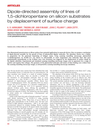
  • 1. Dipole-directed assembly of lines of 1,5-dichloropentane on silicon substrates by displacement of surface charge K. R. HARIKUMAR1 , TINGBIN LIM1 , IAIN R McNAB1 , JOHN C. POLANYI1 *, LINDA ZOTTI2 , SERGE AYISSI2 AND WERNER A. HOFER2 1 Department of Chemistry and Institute of Optical Sciences, University of Toronto, 80 St George Street, Toronto, Ontario M5S 3H6, Canada 2 Surface Science Research Centre, University of Liverpool, Liverpool L69 3BX, UK *e-mail: jpolanyi@chem.utoronto.ca Published online: 30 March 2008; doi:10.1038/nnano.2008.65 One-dimensional nanostructures at silicon surfaces have potential applications in nanoscale devices. Here we propose a mechanism of dipole-directed assembly for the growth of lines of physisorbed dipolar molecules. The adsorbate chosen was a halide, in preparation for the patterned imprinting of halogen atoms. Using scanning tunnelling microscopy, physisorbed 1,5-dichloropentane on Si(100)-231 was shown to self-assemble at room temperature into molecular lines that grew predominantly perpendicular to the Si-dimer rows. Line formation was triggered by the displacement of surface charge by the dipolar adsorbate. Experimental and simulated scanning tunnelling microscopy images were in agreement for a range of positive and negative bias voltages. The geometry of the physisorbed molecules and nature of their binding were evident from the scanning tunnelling microscopy images, as interpreted by scanning tunnelling microscopy simulation. Over the last decade many systems have been identified that yield self-assembled atomic or molecular lines on semiconductors. All these nanolines were formed as a result of covalent bonding within or at the surface. Here we describe a method for the formation of self-assembled molecular lines at room temperature on a bare Si(100)-2Â1 surface using the novel approach of dipole-directed assembly (DDA), shown here for 1,5-dichloropentane (DCP). The adsorbate DCP was chosen because the Cl...Cl separation in a favoured configuration is $4 A˚ , closely matching the 3.8 A˚ Si...Si separation between adjacent Si-dimer pairs, hence offering the possibility of physisorption in a bridging configuration, with the Cl atoms located over adjacent Si atoms. The method has also been applied in initial studies on 1-chloropentane, 1-fluoropentane and 1-chlorododecane. Earlier works report the study of bismuth nanolines1–6 and rare- earth silicide nanowires7–16 on Si(100)-2Â1 using scanning tunnelling microscopy (STM). These lines, of up to 500 nm in length, grew perpendicular to the Si-dimer rows. The lines were formed at high substrate temperatures, $600 8C, by sub-surface reconstruction induced by covalent bonding. Shorter nanolines formed on Si(100) from group II, III and IV metals (for example, Mg, Al and Sn) have also been reported17–23 . Lines of physisorbed molecules have been self-assembled through intermolecular hydrogen-bonding on smooth graphite (see, for example, ref. 24) and metal surfaces (see, for example, ref. 25) but not on Si(100). Chemical chain reactions have also been used to grow nanolines26–30 . Growth occurred along26–28 and across29,30 the dimer rows of H-terminated Si(100), initiated from a dangling-bond site26–30 . Recently, self-assembled molecular lines were formed on a bare Si(100)-2Â1 surface perpendicular to the dimer rows31 , using a surface chain reaction initiated by pyrazine. The adsorbate of the present work, DCP, has been shown by ab initio calculation to result in a dipole at the surface and to induce buckling of the Si-dimer pair of an adjacent row. This buckling favours the adsorption of a molecule at the buckled site. The second adsorbate molecule induces a further buckling in the next Si-dimer row and hence a new site favouring molecular adsorption, and so on, thereby propagating a line of intact physisorbed molecules, as observed. The direction of line growth is invariably opposite to the direction of the dipole. The predominant unidirectionality of the line growth is not explained ab initio; it is likely to have its origin in the tendency for the relief of surface strain to take place linearly along an axis of symmetry32–35 . According to both theory and our STM experiments, the DCP molecules physisorbed at room temperature with their terminal Cl atoms interacting with adjacent Si-dimer atoms to one side of the same dimer row (that is, asymmetrically). The DCP molecular lines self-assembled unidirectionally in the direction of their asymmetric point of attachment, and thus opposed to the direction of the C–Cl dipoles. The direction of line growth was predominantly perpendicular to the dimer rows. Simulations matched the STM images for both empty- and filled-state (positive and negative surface bias) images. Comparison of the STM images with the simulations yielded the adsorption geometry of the molecules and therefore the origin of the likely physisorptive interactions, C–Cl...Si, binding the DCP to Si atoms at the underlying surface. A recent theoretical study36,37 of the interactions of dipolar molecules with Si(100)-2Â1 at high coverages of 0.5 and ARTICLES nature nanotechnology | VOL 3 | APRIL 2008 | www.nature.com/naturenanotechnology222 © 2008 Nature Publishing Group
  • 2. 1.0 monolayers predicted four types of important surface effects resulting in a preference for molecular absorbtion on neighbouring Si dimers of the row. However, these workers discounted the possibility of interaction between adjacent dimer rows, which is central to the present work. RESULTS AND DISCUSSION Figure 1a shows an STM image of Si(100)-2Â1 exposed to 1 L (uncorrected; see Methods for definition of units Langmuir) of 1,5-DCP at room temperature. Intact molecules physisorbed onto the Si surface and self-assembled to form lines predominantly perpendicular to the dimer rows. Approximately 5% of the lines grew diagonally. The molecule–molecule separation distance was 7.7 A˚ , in agreement with the long axis of the Si(100)-2Â1 unit cell. The nanolines consisted of 4–6 molecules on average, 40–50 A˚ long and 4 A˚ wide. Lines were, however, observed with up to 12 molecules (90–100 A˚ long). Increased line length required low dose rates (see later). The STM images suggest that the individual DCP molecules changed their C–Cl bond direction under the influence of the surface to align their Cl atoms with two Si-dimer atoms, one from each adjacent dimer pair to one side of a dimer row, as shown in Fig. 1b. The width of the DCP lines is comparable with the dimer–dimer distance along a row, that is, 3.8 A˚ . This structure was confirmed by the ab initio calculations presented below. The bright features characteristic of the physisorbed molecules did not bridge the dimer rows (Fig. 1c,d). This is in contrast to the molecular lines formed by pyrazine on bare Si(100)-2Â1 midway between two dimer rows, because the pyrazine adsorbate was bound covalently to the adjacent rows31. The DCP lines have an experimental height of 0.7 A˚ for 23 V (Fig. 1f). This agrees with the simulation, which suggests protrusions of $0.8 A˚ in the density contour for this voltage. The DCP molecules involved in DDA physisorbed and self- assembled intact. The evidence for physisorption of intact DCP was that the molecular lines desorbed at elevated temperature (.$ 200 8C), leaving no residue at the surface. In contrast, a covalently bound Si–Cl bond formed by reaction at the surface Diagonal lines –3.0 V Distance (Å) Height(Å) B B A A 1.8 1.6 1.4 1.2 4 8 12 16 0.7 Å –3.0 V –3.0 V Top view Line Side view 1,5-DCP 4 Å Figure 1 Self-assembled molecular nanolines at room temperature. a, A room-temperature STM image (270 Â 270 A˚ ) of a Si(100)-2Â1 surface exposed to 1 L nominally (an uncorrected pressure of 5 Â 1029 torr, 200 s) of DCP. Lines of DCP are imaged as bright features mostly perpendicular to the Si-dimer rows, but with $5% at 26º to the dimer rows (example circled). The direction of line growth is known, and is shown for several cases by white arrows. Individual DCP features (bright protrusions) lie to one side of the dimer rows. b, Perspective and top views (left inset). Black dashed lines denote the centre of the Si-dimer rows throughout, blue spheres denote Cl atoms and blue dotted lines the physisorption interaction. The black arrows indicate the adsorbate dipoles and the long red arrow points in the direction of line growth. A model of 1,5-DCP is shown in the right inset. c, Close-up (60 Â 40 A˚ ) of the nanoline taken from the white rectangle in a. d, Same view as in panel c. Red and black ellipses denote dimers and defects, respectively, black-dashed and grey lines indicate the centre of the ridges and the valleys of the dimer rows. From this picture it is evident that the molecular features (bright protrusions) lie to one side of the dimer rows (to the right as we have oriented panels c–e). A height profile taken along the blue line in the STM image e is shown in f. The point ‘A’ in the linescan denotes a Si dimer, and the highest point in profile ‘B’ corresponds to the midpoint of the molecular feature in this line. At this bias (23 V), the average height of the molecular feature with respect to the Si dimer is 0.7 A˚ . The dark features in the STM images are due mainly to missing-dimer defects. ARTICLES nature nanotechnology | VOL 3 | APRIL 2008 | www.nature.com/naturenanotechnology 223 © 2008 Nature Publishing Group
  • 3. will desorb only above 500 8C (refs 38, 39, 40). Further, DCP molecular lines were thermally stable up to $200 8C. Above 200 8C, over time, a fraction underwent reaction, severing a C–Cl bond to give Cl–Si at the surface, characterized by circular bright spots in the STM image. The bright spots were the Si dangling bonds adjacent to a reacted Cl (Cl–Si). The remainder of the DCP adsorbate desorbed from the surface at 200 8C without chemical reaction, leaving no residue, as expected for a physisorbed molecule. As noted, higher dose rates gave shorter lines, and lower dose rates longer lines; dosing at 1 Â 1029 torr produced lines of 8–10 molecules, whereas 1 Â 1028 torr gave lines of 3–5 molecules. The STM images indicated that the lines invariably originated in dimeric DCP, (DCP)2, a characteristic large bright feature evident at the head of the line in Fig. 2. At the highest dose rate only this bright feature was observed. Previously, we found that chloroalkanes on Si(111)-7Â7 predominantly formed dimers at high dose rates, physisorbing horizontally on Si(111)-7Â7 and Si(100)-2Â1 in contact with the surface41 . This geometry gave additional binding from the contact of CH2 with the underlying Si surface, rendering the horizontal molecules more stable in their adsorbed state42–44 . On heating, the dimeric (DCP)2 was found, as expected from its multiple points of attachment, to be more strongly bound to the surface than the monomer. In the present experiment, line length was limited by a kinetic competition between dimer formation (the start of a new line) and attachment of a monomer to an existing line (resulting in line growth). Because of the quadratic dependence on monomer concentration for dimer formation45 , high dose rates favoured the formation of many dimers, and hence shorter lines. At room temperature, we observed no features that could be ascribed to single monomeric DCP molecules in the adsorbed state, due, presumably, to their high mobility. The observed molecular lines originated in a stable (DCP)2 dimer—the ‘anchor’ for that line. The lines propagated through linear self-assembly of a succession of DCP monomers, which, although unstable individually, were highly stable when self-assembled, even at elevated temperatures up to $200 8C. At high resolution the lines in the room-temperature images gave evidence of terminating in a raised surface feature (Fig. 2), in agreement with expectations from the DDA model, presented in the following sections. In other experiments DCP was dosed at a 100 8C Si(100)-2Â1 surface using the same dose rate as in the room-temperature experiments. No nanolines were observed. Instead, reaction took place to yield exclusively halogen atoms. Once again, the remainder of the DCP molecule desorbed. Dosing at 100 8C gave a smaller coverage, in this case of Cl–Si, by a factor of between 10 and 12, than an equivalent dose at room temperature, indicating that the sticking probability was lower by this amount as compared with that at room temperature. In Fig. 2a we show a high-resolution image of a single DCP line. The anchor, the DCP dimer (DCP)2, is clearly visible, as are the individual DCP molecules in the line, and also the Si surface dimers and back bonds. The end of the line shows a severe perturbation of the Si dimers. Theory suggests that this perturbation is due to buckling of the surface originating in the dipole of the adsorbate (hence ‘dipole-directed assembly’) encouraging the adsorbtion of a further DCP molecule and so continuing line growth. Line growth is limited here by DCP coverage. Figure 2c to f shows STM images of another DCP line, obtained with different negative and positive sample biases (left and right, respectively). The appearance of the line can be seen to be highly voltage-dependent. The corresponding left and right images were taken simultaneously with opposite biases in alternate line scans. In the filled state (negative surface bias, Fig. 2d and f), as the magnitude of bias was increased the lines brightened. At sufficiently high negative bias, starting at 22 V (not shown), the molecular lines were brighter than the Si-dimer rows; at lower negative biases they appeared darker than the Si-dimer rows. The +1.0 V Direction of line growth B Xʹ B 40 X (Å) Z (Å) 30 20 10 0 1.2 0.8 0.4 0 X +1.0 V +0.6 V +1.5 V –1.5 V –0.6 V A B Aʹ Bʹ A A B B A B Aʹ Bʹ Aʹ Bʹ Aʹ Bʹ DCP2 DCP2DCP2 DCP2 Figure 2 STM images of single nanolines. a, High-resolution image (50 Â 30 A˚ ) of a single DCP line with a line height profile (inset) taken along the line X–X0 ; the circled feature ‘B’ is the perturbation at the end of the line due to surface buckling. b, The image of panel a reproduced with ball and stick molecules superimposed, to scale, of (DCP)2 and DCP over the corresponding features of the image. c–f, STM images (85 Â 60 A˚ ) of a further single DCP line at positive and negative voltages; panels c and d were recorded simultaneously as were panels e and f. An additional DCP dimer (unlabelled) is visible at the left, adjacent to the line. The white lines A–A0 and B–B0 marked in each image represent the same features, the ridges of adjacent dimer rows in c–f. In positive bias the DCP line always appears bright relative to the dimer rows. The positive-bias images (c and e) show the well-known contrast reversal at and above þ1.5 V bias; A–A0 and B–B0 then appear as valleys rather than ridges. In negative-bias images the DCP line appears dark relative to the dimer rows, brightening as the bias goes to larger negative values. The direction of line growth is indicated by white arrows; line growth can be seen to begin with a DCP dimer (DCP)2. Dark trenches are observed to both sides of the DCP lines of bright molecules; this is due to pinning of adjacent dimers (see text and Fig. 4). At high bias (positive and negative), the DCP dimers can be seen to be almost indistinguishable from individual DCP molecules. ARTICLES nature nanotechnology | VOL 3 | APRIL 2008 | www.nature.com/naturenanotechnology224 © 2008 Nature Publishing Group
  • 4. bright features comprising the lines of DCP in the STM images are calculated to be primarily due to the contribution from the alkyl chains made visible by the attached halogen atoms46,47 . Figure 2c,e shows the well-known contrast reversal, in which the ridge of a dimer row appears bright below 1.5 V and dark above 1.5 V surface bias48–50 . DENSITY FUNCTIONAL THEORY CALCULATIONS To understand the formation of molecular lines on the surface we performed extensive density functional theory (DFT) simulations (see Methods). In Fig. 3 we show the details of the computed mechanism for line propagation. Figure 3b shows the state of the Si dimers p(2Â2) on Si(100), which is in an unperturbed up– down Si-dimer pair configuration. The up and down Si atoms in the Si dimers are colour-coded red (up) and dark green (down). Generally, this configuration corresponds to an excess (up) and a depletion (down) of electron charge (see, for example, ref. 51). The two Si-dimer pairs of interest, on which the Cl atoms of the first DCP will physisorb, are labelled 1B0 and 1C0 . The adsorption energy using a linear molecule in vacuum as the reference is 2.6 eV per molecule. The energy required to change the C–Cl bond direction from that in the gas-phase molecule to the configuration on the surface is approximately 0.2 eV. Calculation of a DCP dimer clearly showed buckling of the adjacent Si-dimer pair, as for the DCP monomer. Details of (DCP)2 interaction with the surface will be published as part of a study of dimeric adsorbates and their DDA. The present discussion focuses on the (novel) mechanism of DCP monomer line propagation. The attachment of a single DCP molecule at 1B0 and 1C0 on row 1 leads to a dipole, both because of a charge transfer from the Cl atoms of the DCP to adjacent Si dimers and the induced dipole of the molecule in its adsorbed configuration. This net dipole is directed perpendicular to the Si-dimer rows with a dipole strength of 4.85 D (debye) indicated by black arrows in Fig. 3 (we use the convention that the arrows point from positive to negative in the dipole). Figure 3c shows buckling of the Si dimers resulting from the adsorption of this first molecule. The computed charge redistribution consequent on DCP physisorption is shown in Fig. 3e; electron density has moved from the Cl atoms (adsorbed at Si atoms 1B0 and 1C0 ) to the other Si atoms of the same dimer pairs, 1B and 1C, which, consequently, are raised to the ‘up’ configuration (see previous paragraph). Owing to the electrostatic interaction between the dipole and the Si atoms of the adjacent row, no. 2 in Fig. 3, dimers 2A, 2A0 ; 2B, 2B0 and 2C, 2C0 flip as shown in Fig. 3c. This may be assisted by the inter-row charge transfer evident as ‘tails’ in the negative charge gain (G) at the right of Fig. 3e (ii). The Si-dimer reorientation leads to an energy gain of 140 meV and provides a preferential adsorption site for the next molecule in its mobile precursor state. Supercell 1,5-DCP Si dimer Up 1A 1B 1Aʹ 1Bʹ 2B 2Bʹ 2A 2Aʹ 3A 3B 3Aʹ 3Bʹ 1C 1Cʹ 2C 2Cʹ 3C 3Cʹ 1A 1B 1Aʹ 1Bʹ 2B 2Bʹ 2A 2Aʹ 3A 3B 3Aʹ 3Bʹ 1C 1Cʹ 2C 2Cʹ 3C 3Cʹ 1A 1B 1Aʹ 1Bʹ 2B 2Bʹ 2A 2Aʹ 3A 3B 3Aʹ 3Bʹ 1C 1Cʹ L i ii Loss (L) Gain (G) CI DB L 1B 1C G G G G 2C 2Cʹ 3C 3Cʹ Down Figure 3 Mechanism of formation of the molecular line (theory). a, Schematic representation of the dipoles (short black arrows) responsible for buckling of the dimers. The locations of the molecules are represented by golden ellipses. The grey box represents the supercell slab used for the calculation. The black dashed lines denote the centres of the Si-dimer rows. The 1,5-DCP molecule and the colour-coded ‘up’ and ‘down’ Si dimer atoms are shown. b, Ground-state Si(100)-p2Â2 surface. The dimer pairs are numbered 1A–1A0 , 1B–1B0 and 1C–1C0 in the left dimer row, 2A–2A0 , 2B–2B0 and 2C–2C0 in the adjacent dimer row and 3A–3A0 , 3B–3B0 and 3C–3C0 in the third dimer row. The ‘up’ and ‘down’ dimers are colour-coded red and green. c, The computed buckling due to adsorption of a single molecule on row 1. The bonded Si atoms 1B0 and 1C0 are down, and 1B and 1C are up. In row 2, 2B0 and 2C0 are up, 2B and 2C are down. The brackets indicate favoured pairs of adsorption sites for the second DCP molecule. d, Attachment of the second molecule in row 2 repeats for rows 2 and 3 the process of surface-buckling shown for rows 1 and 2 in c. The third adsorbate molecule (not shown) will attach to the bracketed Si atoms collinear with the first two dipolar adsorbate molecules. e, Charge redistribution on adsorption of a DCP molecule. (i) Loss (L) in electronic density within the white contour shown (20.004e A˚ 23 ) and (ii) gain (G) in electronic density within the white contour (þ0.004e A˚ 23 ). Colour coding is as in the other panels. Cl indicates the approximate location of the halogen atom losing negative charge, and DB the location of the Si dangling bond (1B and 1C) gaining charge. The black dashed line denotes the centres of the Si dimer rows. ARTICLES nature nanotechnology | VOL 3 | APRIL 2008 | www.nature.com/naturenanotechnology 225 © 2008 Nature Publishing Group
  • 5. The second DCP molecule can only attach at the elevated Si atoms (2B0 , 2C0 ) due to steric hindrance from the first DCP. Subsequently the pair of Si atoms 2B0 , 2C0 move down (Fig. 3d, green). This is accompanied by further reorientation at the adjacent Si-dimer row 3, with elevation of Si atoms 3B0 and 3C0 , preparing a raised site for attachment of a third DCP (Fig. 3d, bracketed red atoms). The sequence then continues until the system either runs out of adsorbate or encounters a defect. A second DCP molecule migrating across the surface could, alternatively (Fig. 3c) attach at the pair of Si atoms labelled 2A0 (raised) and 2B0 (raised). A growth direction perpendicular to the dimer rows is energetically favoured due to dipole interactions by about 80 meV per molecule relative to diagonal line growth. The difference in the adsorption energy is sufficient to make diagonal growth only $5% as likely as perpendicular growth, at room temperature, as is observed. In the presence of two adsorbate molecules (Fig. 3d), line growth in general proceeds collinearly with these molecules; that is, the lines rarely wander from their initial propagation direction. A likely explanation is a tendency for strain to relieve itself linearly in the surface34–37. However, the growth of the line beyond two DCP molecules is beyond the limit of our supercell, and hence not calculable. In summary, adsorbed molecules induce substantial dipoles (shown as black arrows pointing to the left in Fig. 3), which result from charge transfer to the surface and the dipole of the distorted DCP. Electrostatic interactions with this net dipole pin the Si dimers on the adjacent Si-dimer row, to the right in the figure, into their new configuration as detailed above, and propagate the line through self-assembly of additional DCP monomer molecules away from the direction of the initial induced dipole. This is the mechanism for DDA. STM SIMULATIONS In Fig. 4 we compare the simulated STM image with the experimental constant-current (0.2 nA) STM images at a sample bias of +0.6 V. The calculated images reproduce the observation of a tip–surface distance of 6–7 A˚ . Images were simulated using a metal tip with a mono-atomic apex at a current of 0.2 nA (negative bias) and 0.1 nA (positive bias). The current contour in the positive regime is closer to the surface, so we had to decrease the contour value to obtain a closed contour surface (see Methods). Because the 4 Â 4 supercell is too small to describe the boundary between the molecular lines and the dimer rows, we used a 4 Â 6 supercell in all simulations. To analyse the effect of dimer buckling adjacent to the molecular rows we varied the supercell boundary. The Si dimers have the correct up–down orientation on one side (above, in the simulations of Fig. 4), but are flipped in the opposite direction on the other side (below, in the simulations of Fig. 4). At higher negative bias voltages (images not shown) we find that the protrusion due to the adsorbed molecules had its maximum at the position of the Cl atoms. The computed images in Fig. 4d have darkness above the molecular line (X–X0 ) and brightness below (Y–Y0 ). The calculated darkness is due to the Si dimer being buckled in the opposite sense to the rest of its row, as shown in the blue- bounded insert. Brightness indicates that the Si dimer is buckled in the same sense as the rest of its row. Experimentally, in both positive and negative STM images at low bias (+0.6 V; Fig. 4b,e), we observed darkness at both sides of the line. It would appear that the dimers on both sides of the molecular rows are pinned, and the rest of the rows appear bright due to averaging of dimer positions at room temperature. +0.6 V, 0.1 nA –0.6 V, 0.2 nA –0.6 V, 0.2 nA +0.6 V, 0.2 nA X Y Xʹ Yʹ Theory Experiment Experiment + Theory Figure 4 Comparison between theoretical and experimental images. a,d, Simulated STM images of DCP molecules arranged in lines on Si(100)-p(2Â2) at þ0.6 V (a) and 20.6 V (d) bias. Each rectangle in the grid represents a 2 Â 1 unit cell (two of which are highlighted by blue rectangles in d, with up and down Si atoms coloured red and green); DCP molecules are drawn to scale at the right in the simulated images. The centres of the dimer rows in the simulated images are indicated by dashed lines (corresponding to the ridges of the dimer rows in the experimental images). In the simulated image of the empty state (a), bright protrusions are visible at the location of the Cl atoms. b,e, Images recorded at the same bias as the simulations (a,d); the appearance of the lines in the simulated images matches well with the appearance of the lines in the experimental STM images at the same bias. For the positive-bias image, theoretical simulations were made at half the experimental current (0.1 nA rather than 0.2 nA) so the features due to DCP appear enlarged relative to the experimental image. c,f, The simulated lines are shown superimposed on the experimental images. The dark arrows X–X0 and Y–Y0 in d show a line of darkness above the molecular line and a line of brightness below the molecular line (see text). The filled-state STM image at 20.6 V is shown in e; the lines appear darker at this bias, which matches the simulated image d. ARTICLES nature nanotechnology | VOL 3 | APRIL 2008 | www.nature.com/naturenanotechnology226 © 2008 Nature Publishing Group
  • 6. CONCLUSIONS We report a novel DDA mechanism for the formation of physisorbed molecular lines at room temperature on a Si(100)-2Â1 surface, as observed by STM and modelled by DFT calculation. Self-assembly resulted in lines of intact 1,5-DCP monomers of up to 12 molecules aligned predominantly perpendicular to the dimer rows, with a 5% minority at a 268 angle to the rows. Once a pair of molecules established a line direction, that direction was generally observed to be maintained invariable for all subsequent molecules in the line. The mechanism of line propagation of DCP monomers was shown by DFT calculation to originate in the dipole of an adsorbed molecule, molecule 1, attached by its two halogen atoms to adjacent Si atoms along a dimer row. The dipole- induced charge transfer in the surface is perpendicular to the Si-dimer row. This transfer of charge resulted in buckling of adjacent dimer pairs in row 2, giving rise to an attractive site for molecule 2. A second DCP monomer was adsorbed adjacent to the first, further shifting the surface charge, thereby buckling row 3 and capturing a third DCP molecule along the extension of the line formed by the first two, so propagating the line. At room temperature, DCP monomers are mobile on Si(100)-2Â1. Line growth originated in a single dimer of (DCP)2 (the anchor) through subsequent collinear assembly of the mobile DCP monomers. In the STM images the constituent DCP molecules of the line were displaced to the same side of successive Si-dimer rows as the direction of line growth, in agreement with theory. This direction of line growth by DDA is opposite to the direction of the individual DCP dipoles. Where line growth was limited by coverage, surface-buckling could be seen by STM in the Si-dimer row beyond the final DCP molecule of the line. Line termination was also observed to occur due to defective assembly, occasioned by a second dimer or by a surface defect. A requirement for DDA is that the initial adsorbate molecule has a preferred adsorbate alignment on the surface and a dipole moment when adsorbed. The orientation of the adsorbate dipole, through the mediation of surface charge transfer, is opposite to the propagation direction of the self-assembled line. Further requirements are that the substrate be electrically polarizable, and that subsequent molecules to the first be sufficiently mobile to self-assemble. Charge transfer in the surface manifests itself, in the present case, as a buckling of the Si atoms of an adjacent dimer row of Si(100)-2Â1. The physisorbed dipolar molecular lines observed in this work were stable up to temperatures of $200 8C, without desorption or chemical reaction. The finding that mobile dipolar adsorbates can self-assemble into such robust lines under the influence of charge transfer to or from the substrate should be of interest in contexts ranging from nanoscale electronics to molecular biology. METHODS EXPERIMENTAL METHODS Experiments were carried out at room temperature in ultrahigh vacuum (UHV) using two STM instruments (RHK400 and Omicron-VT) using phosphorous- doped (n-type, 0.01–0.02 V.cm, 250+25 mm thick) Si(100) reconstructed to give Si(100)-2Â1. The adsorbate 1,5-DCP (99.9 % pure, Aldrich) was subjected to repeated freeze–pump–thaw cycles before being introduced to the UHV chamber through a leak valve for background dosing. Exposures are reported in Langmuir (1 L ¼ 1 Â 1026 torr s) measured with an uncorrected ion-gauge calibrated for N2. The corrected doses would be $10 times lower than the stated doses52. The STM tips were made by a d.c. electrochemical etch of polycrystalline tungsten wire in a 2 M NaOH solution. The scanning tunnelling microscopes were operated in the constant-current mode. All measurements were made with a tunnelling current of 0.2 nA. Samples were cleaned in UHV by several cycles of d.c. heating to 1,240 8C for $1 min. The STM images of the surface cleaned in this way showed a (2 Â 1) reconstruction and , 0.2% surface defects. ELECTRONIC STRUCTURE SIMULATIONS The ground-state electronic structure of one or two molecules on Si(100) was simulated with the Vienna Ab initio Simulation Package (VASP)53,54 using ultrasoft pseudopotentials and the PW91 parameterization55 of the exchange- correlation potential. The Si(100) slab contained eight layers, the bottom layer of which was passivated with hydrogen. We simulated 4 Â 4 and 4 Â 6 supercells, retaining the p(2Â2) arrangement of the buckled dimers. The high number of layers was necessary to represent the high elasticity of the silicon lattice. Owing to the large number of atoms, we limited the simulations of the relaxed geometry to one k-point at the centre of the surface brillouin zone. The molecular adsorption site was determined by placing the bent molecules about 3 A˚´ above the surface plane, with the molecular backbone parallel to the surface. The molecule, as well as three surface layers, were then fully relaxed until the forces on individual ions were less than 0.02 eVA˚´ 21 . The molecular adsorption sites for one- and two-monomer DCP molecules in a 4 Â 4 and 4 Â 6 Si(100) supercell were calculated using several supercells: a single DCP molecule in a 4 Â 4 supercell, two molecules in alignment perpendicular to the dimer rows, two molecules in diagonal alignment, and the same three arrangements of molecules in a 4 Â 6 supercell. The alignment of adsorbate molecular dipoles is shown schematically in Fig. 3a. The grey box represents the supercell slab used for the calculation (not the surface unit cell). CALCULATION OF DIPOLES DFT calculation gives a zero dipole for the symmetric linear DCP molecule in the gas. The dipoles were calculated for a single molecule on the Si(100)-4Â4 supercell using the dipole corrections implemented in our electronic structure code. For this simulation we first calculated the electron density of the molecules in the vacuum, then the density of the clean Si surface and finally the density of the complete system. Subtracting the density of the components from the density of the complete system yielded the charge transfer due to adsorption. The position of the dipole was subsequently placed at the median position between positive and negative charge accumulation, and the dipole moment was calculated using dipole corrections in (only) two dimensions along the surface plane. We found a dipole moment of 4.85 D per molecule perpendicular to the dimer rows. SIMULATION OF STM IMAGES The STM images for a current of 200 pA (negative bias) or 100 pA (positive bias) and a range of bias voltages were simulated using the electronic structure of the converged system, and the multiple scattering approach implemented in bSKAN56,57 . To improve the accuracy we used a k-point set of 3 Â 3 special k-points in the final electronic structure simulations, as also for the STM simulations. To obtain a closed contour surface in the simulation, the current value in the positive bias regime had to be reduced. Received 20 September 2007; accepted 27 February 2008; published 30 March 2008. References 1. Naitoh, M., Shimaya, H., Nishigaki, S., Oishi, N. & Shoji, F. Scanning tunneling microscopy observation of bismuth growth on Si(100) surfaces. Surf. Sci. 377–379, 899–903 (1997). 2. Naitoh, M., Shimaya, H., Nishigaki, S., Oishi, N. & Shoji, F. Scanning tunneling microscopy observation of Bi-induced surface structures on the Si(100) surface. Surf. Sci. 482–485, 1440–1444 (2001). 3. Owen, J. H. G., Miki, K. & Bowler, D. R. Self-assembled nanowires on semiconductor surfaces. J. Mater. Sci. 41, 4568–4603 (2006). 4. MacLeod, J. M. & McLean, A. B. Single 2 Â 1 domain orientation on Si(100) surfaces using a periodic Bi line arrays. Phys. Rev B 70, 041306 (2004). 5. MacLeod, J. M., Miwa, R. H., Srivastava, G. P. & McLean, A. B. The electronic origin of contrast reversal in bias-dependent STM images of nanolines. Surf. Sci. 576, 116–122 (2005). 6. Preinesberger, C., Vandre, S., Kalka, T. & Dahne-Preitsch, M. Formation of dysprosium silicide wires on Si(001) . J. Phys. D 31, L43–L45 (1998). 7. Chen, Y., Ohlberg, D. A. A. & Williams, R. S. Nanowires of four epitaxial hexagonal silicides grown on Si(001). J. Appl. Phys. 91, 3213–3218 (2002). 8. Nogami, J., Liu, B. Z., Katkov, M. V., Ohbuchi, C. & Birge, N. O. Self-assembled rare earth silicide nanowires on Si(001). Phys. Rev. B 63, 233305 (2001). 9. Liu, B. Z. & Nogami, J. Growth of parallel rare earth silicide nanowire arrays on vicinal Si(001). Nanotechnology 14, 873–877 (2003). 10. Liu, B. Z. & Nogami, J. An STM study of the Si(001)(2Â4)-Dy surface. Surf. Sci. 488, 399–405 (2001). 11. Ohbuchi, C. & Nogami, J. Holmium growth on Si(001): Surface reconstructions and nanowire formation. Phys. Rev. B 66, 165323 (2002). 12. Katkov, M. V. & Nogami, J. Yb and Nd growth on Si(001). Surf. Sci. 524, 129–136 (2003). ARTICLES nature nanotechnology | VOL 3 | APRIL 2008 | www.nature.com/naturenanotechnology 227 © 2008 Nature Publishing Group
  • 7. 13. Ohbuchi, C. & Nogami, J. Samarium induced surface reconstructions of Si(001). Surf. Sci. 579, 157–165 (2005). 14. Harrison, B. C. & Boland, J. J. Real-time STM study of inter-nanowire reactions: GdSi2 nanowires on Si(100). Surf. Sci. 594, 93–98 (2005). 15. Evans, M. M. R. & Nogami, J. Indium and gallium on Si(001): A closer look at the parallel dimer structure . Phys. Rev. B 59, 7644–7648 (1999). 16. Nogami, J., Baski, A. A. & Quate, C. F. Aluminum on the Si(100) surface: Growth of the first monolayer. Phys. Rev. B 44, 1415–1418 (1991). 17. Glueckstein, J. C., Evans, M. M. R. & Nogami, J. Growth of Sn on Si(001) at room temperature. Surf. Sci. 415, 80–94 (1998). 18. Itoh, H., Tanabe, H., Winau, D., Schmid, A. K. & Ichinokawa, T. Growth mode and surface structures of the Pb/Si(001) system observed by scanning tunneling microscopy. J. Vac. Sci. Tech. B 12, 2086–2089 (1994). 19. Tomatsu, K., Nakatsuji, K., Iimori, T. & Komori, F. STM observation of initial growth of Sn atoms on Ge(001) surface. Surf. Sci. 601, 1736–1746 (2007). 20. Hutchison, P., Evans, M. M. R. & Nogami, J. Mg growth on the Si(001) surface: An STM study. Surf. Sci. 411, 99–110 (1998). 21. Bakhtizin, R. Z., Kishimoto, J., Hashizume, T. & Sakurai, T. STM study of Sr adsorption on Si(100) surface. Appl. Surf. Sci. 94, 478–484 (1996). 22. Bird, C. F. & Bowler, D. R. A spin polarized first-principles study of short dangling bond wires on Si(001). Surf. Sci. 531, L351–L355 (2003). 23. Chen, T. C. et al. Atomic-scale desorption through electronic and vibrational excitation mechanisms. Science 268, 1590–1592 (1995). 24. Cyr, C. M., Venkataraman, B. & Flynn, G. W. Functional group identification in scanning tunneling microscopy of molecular adsorbates. J. Phys. Chem. 100, 13747–13759 (1996). 25. Canas-Ventura, M. E. et al. Coexistence of one- and two-dimensional supramolecular assemblies of terephthalic acid on Pd(111) due to self-limiting deprotonation. J. Chem Phys. 125, 184710 (2006). 26. Lopinski, G. P., Wayner, D. D. M. & Wolkow, R. A. Self-directed growth of molecular nanostructures on silicon. Nature 406, 48–51 (2000). 27. DiLabio, G. A., Piva, P. G., Kruse, P. & Wolkow, R. A. Dispersion interactions enable the self-directed growth of linear alkane nanostructures covalently bound to silicon. J. Am. Chem. Soc. 126, 16048–16050 (2004). 28. Kruse, P., Johnson, E. R., DiLabio, G. A. & Wolkow, R. A. Patterning of vinylferrocene on H–Si(100) via self-directed growth of molecular lines and STM-induced decomposition. Nano Lett. 2, 807–810 (2002). 29. Hossain, M. Z., Kato, H. S. & Kawai, M. Controlled fabrication of 1D molecular lines across the dimer rows on the Si(100)-(2 Â 1)-H surface through the radical chain reaction. J. Am. Soc. Chem. 127, 15030–15031 (2005). 30. Hossain, M. Z., Kato, H. S. & Kawai, M. Fabrication of interconnected 1D molecular lines along and across the dimer rows on the Si(100)-(2 Â 1)-H surface through the radical chain reaction. J. Phys. Chem. B 109, 23129–23133 (2005). 31. Shimomura, M. et al. Formation of one-dimensional molecular chains on a solid surface: Pyrazine/Si(001). Phys. Rev. B 72, 033303 (2005). 32. Wang, Y., Chen, X. & Hamers, R. J. Atomic-resolution study of overlayer formation and interfacial mixing in the interaction of phosphorus with Si(001). Phys. Rev. B 50, 4534–4547 (1994). 33. Kipp, L. et al. Adsorption and decomposition on Si(100) 2 Â 1 studied by STM . Phys. Rev. B 52, 5843–5850 (1995). 34. Knall, J. & Pethica, J. B. Growth of Ge on Si(100) and Si(113) studied by STM. Surf. Sci. 265, 156–167 (1992). 35. Park, Ch., Bakhizin, R. Z., Hashizume, T. & Sakurai, T. Strain relief and ordering of (2 Â n)-Bi structure on Si(100). J. Vac. Sci. Technol. B 12, 2049–2051 (1994). 36. Wang, Y. & Hwang, G. S. Two-dimension arrangement of CH3NH2 adsorption on Si(001)-2Â1. Chem. Phys. Lett. 385, 144–148 (2004). 37. Wang, Y. & Hwang, G. S. Origin of nonlocal interactions in adsorption of polar molecules on Si(001)-2Â1. J. Chem. Phys. 122, 164706 (2005). 38. Gao, Q., Cheng, C. C., Chen, P. J., Choyke, W. J. & Yates, J. T. Jr. Chlorine bonding sites and bonding configurations on Si(100)-2 Â 1. J. Chem. Phys. 98, 8308–8323 (1993). 39. Szabo, A., Farrall, P. D. & Engel, T. Reactions of chlorine with Si(100) and Si(111): Adsorption and desorption kinetics. Surf. Sci. 312, 284–300 (1994). 40. Gupta, P., Coon, P. A., Koehler, B. G. & George, S. M. Desorption product yields following Cl2 adsorption on Si(111)-7 Â 7: Coverage and temperature dependence. Surf. Sci. 249, 92–104 (1991). 41. Dobrin, S. et al. Self-assembled molecular corrals on a semiconductor surface. Surf. Sci. 600, 43–47 (2006). 42. Dubois, M., Delerue, C. & Rubio, A. Adsorption and electronic excitation of biphenyl on Si(100): a theoretical STM analysis. Phys. Rev. B 75, 041302 (2004). 43. Grandidier, B. et al. Effect of alkyl substituents on the adsorption of thienylenevinylene oligomers on the Si(100) surface. Surf. Sci. 473, 1–7 (2001). 44. Lei, R. Z., Gellman, A. J. & Koel, B. E. Desorption energies of linear and cyclic alkanes on surfaces: Anomalous scaling with length. Surf. Sci. 554, 125–140 (2004). 45. Dobrin, S. et al. Molecular dynamics of haloalkane corral-formation and surface halogenation at Si(111)-7 Â 7. J. Chem. Phys. 125, 133407 (2006). 46. Grandidier, B. et al. Effect of alkyl substituents on the adsorption of thienylenevinylene oligomers on the Si(100) surface. Surf. Sci. 473, 1–7 (2001). 47. Dubois, M., Delerue, C. & Allan G. Scanning tunneling microscopy and spectroscopy of conjugated oligomers weakly bonded to Si(100) surfaces: A theoretical study. Phys. Rev. B 71, 165435 (2005). 48. Kondo, Y., Amakusa, T., Iwatsuki, M. & Tokomoto, H. Phase transition of the Si(001) surface below 100 K. Surf. Sci. 453, L318–L322 (2000). 49. Lyubinetsky, I., Dohnalek, Z., Choyke, W. J. & Yates, J. T. Jr. Cl2 dissociation on Si(100)-(2 Â 1): A statistical study by scanning tunneling microscopy. Phys. Rev. B 58, 7950–7957 (1998). 50. Okada, H., Fujimoto, Y., Endo, K., Hirose, K. & Mori, Y. Detailed analysis of scanning tunneling microscopy images of the Si(001) reconstructed surface with buckled dimers. Phys. Rev. B 63, 195324 (2001). 51. Oura, K., Lifshits, V. G., Saranin, A. A., Zotov, A. V. & Katayama, M. Surface Science: An Introduction 181–183 (Springer-Verlag, Berlin, 2003). 52. Bartmess, J. E. & Georgiadis, R. M. Empirical methods for determination of ion gauge sensitivities for different gases. Vacuum 33, 149–153 (1983). 53. Kresse, G. & Hafner, J. Ab initio molecular dynamics for liquid metals. Phys. Rev. B 47, 558–561 (1993). 54. Kresse, G. & Furthmu¨ller, J. Efficient iterative schemes for ab initio total-energy calculations using a plane-wave basis set. Phys. Rev. B 54, 11169–11186 (1996). 55. Perdew, J. P. et al. Atoms, molecules, solids, and surfaces: Applications of the generalized gradient approximation for exchange and correlation. Phys. Rev. B 46, 6671–6687 (1992). 56. Hofer, W. A. & Redinger, J. STM of binary alloys: First principles calculation of the current for PtX(100) surfaces. Surf. Sci. 447, 51–61 (2000). 57. Palotas, K. & Hofer, W. A. Multiple scattering in a vacuum barrier obtained from real-space wavefunctions. J. Phys. Condens. Matter 17, 2705–2713 (2005). Acknowledgements The authors are indebted to the Natural Sciences and Engineering Research Council of Canada (NSERC), the Ontario Centers of Excellence (OCE) Centre for Photonics, the Canadian Institute for Photonic Innovation (CIPI), and the Canadian Institute For Advanced Research (CIFAR) for their support. We thank L. Leung for helpful discussions. W.A.H. thanks the Royal Society for financial support. Correspondence and requests for materials should be addressed to J.C.P. Author contributions The experiments were performed jointly by K.R.H., T.L., I.R.M. and J.C.P. at the University of Toronto, and the computations by L.Z., S.A. and W.A.H. at the University of Liverpool. Reprints and permission information is available online at http://npg.nature.com/reprintsandpermissions/ ARTICLES nature nanotechnology | VOL 3 | APRIL 2008 | www.nature.com/naturenanotechnology228 © 2008 Nature Publishing Group