1. Poster template by ResearchPosters.co.za
Copywrite Digital Printers
Poster Template for a 1189mm x 841mm poster presentation
Your name and the names of the people who have contributed to this presentation go here.
The names and addresses of the associated institutions go here.
Introduction
By combining uniquely structured plasmonic metals with stable metal oxides, hot electrons
can be harvested to drive difficult chemical reactions.1 Silver nanowires were used as light
absorbers because of their unique morphology, yielding broader light absorption. Nanowires
with unique structures were made that absorb light in the visible spectrum. With the ability to
create silver nanowires in different morphologies, we hope to find that the plasmonic effect is
amplified due to increased surface area of the nanowires. This could result in a plasmonic
device with increased efficiency for solar to fuel applications.
Motivation
Synthesis Part 1
Nanopores were formed on aluminum
stubstrate with the following process:
• Oxalic acid anodization
• Chromic acid etch
• Oxalic acid anodization
• Phosphoric acic anodization
• Widened in phosphoric acid
for 45 minutes.
Synthesis Part 2
The alumina template was then etched away
using 5 weight percent phosphoric acid
solution for 45 minutes to leave the nanowires
and silica template.
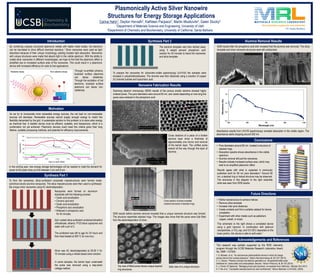
Nanowire Fabrication Results
Alumina Removal Results
Conclusions
Acknowledgements and References
• Refine nanostructure to achieve helices
• Remove silica template
• Increase inter-pore distances
• Create contacts and find a suitable catalyst for device
completion
• Experiment with other metals such as palladium,
copper, cobalt, or nickel
As we try to incorporate more renewable energy sources, the net load on non-renewable
sources will decrease. Renewable sources cannot supply enough energy to match the
flexibility demanded by the grid. A sustainable solution to this problem is to store solar energy
as chemical fuel. A realistic device must be efficient, scalable, and inexpensive, which is a
combination not yet achieved. Plasmonic devices could meet this criteria given their long
lifetime, scalable processing methods, and potential for efficiency improvements.
Plasmonically Active Silver Nanowire
Structures for Energy Storage Applications
Carina Hahn1, Dayton Horvath2, Kathleen Pacpaco2, Martin Moskovits2, Galen Stucky2
1Department of Materials Science and Engineering, University of Utah
2Department of Chemistry and Biochemistry, University of California, Santa Barbara
1. S. Mubeen, et al., “An autonomous photosynthetic device in which all charge
carriers derive from surface plasmons,” Nature Nanotechnology, 8, 247-251 (2013).
To form the nanowires, silica–surfactant composite mesostructures were formed inside
cylindrical anodic alumina nanopores. The silica mesostructures were then used to synthesize
the unique silver nanowires using AC electrodeposition.
Spin coated silica-surfactant contained tetraethyl
orthosilicate, ethanol, P123 block copolymer and
water with a pH of 2.
The surfactant was left to age for 24 hours and
then heat treated at 500 oC for one hour.
Silver was AC electrodeposited at 28.28 V for
10 minutes using a nitrate based silver solution.
This schematic to the right shows a completed device
using a gold nanorod. In combination with platinum
nanoparticles, a TiO2 cap, and CO-OEC deposited on the
lower portion, this device is able to split water.1
SEM results before alumina removal revealed that a unique nanowire structure was formed.
The structure resembles stacked rings. The images also show that the pores were fully filled
from the electrodeposition of silver.
Absorbance results from UV/VIS spectroscopy revealed absorption in the visible region. The
absorbance starts dropping around 550 nm.
SEM results after the phosphoric acid etch revealed that the alumina was removed. The silica
template and silver nanowire structures were left undisturbed.
Through re-emitted photons,
localized surface plasmons
can decay radiatively.
Through the excitation of hot
electrons, localized surface
plasmons can decay non-
radiatively.
In the coming year, new energy storage technologies will be needed to meet the demand for
power at the peak ramp-up time between 4 pm and 8 pm.
This research was partially supported by the RISE internship
program through the UCSB Materials Research Laboratory Award
No. DMR -1121053.
Scanning electron microscopy (SEM) results of the porous anodic alumina showed highly
ordered pores. The pore diameters were around 65 nm, and varied depending on how long the
pores were widened in the phosphoric acid.
Top view of filled pores shows unique layered
ring structures.
Side view of a unique structure.
Cross section of pores revealed
ordered structures of stacked rings.
Cross sections of a piece of a broken
alumina layer show a thickness of
approximately one micron and removal
of the barrier layer. The unfilled pores
extend all the way through the layer of
alumina.
• Pore diameters around 65 nm created a structure of
stacked rings.
• Absorption spectra shows absorbance in the visible
spectrum.
• Alumina removal left just the nanowires
• Results indicate increased surface area, which may
lead to an amplified plasmonic effect
Results agree with what is expected in previously
published work for 60 nm pore diameters.4 Around 60
nm, a stacked ring or helical structure may be observed.
The structures in this diagram to the right resemble
what was seen from SEM results.
Future Directions
4
1
2
3
In some samples, the barrier layer underneath
the pores was removed using a step-down
voltage method.
Radiative decay Non-radiative decay
0.4
0.8
1.2
1.6
300 500 700 900 1100
Absorbance(Au)
Wavelength (nm)
65 nm
2. C. Clavero, “Plasmon-induced hot-electron generation at nanoparticle/metal-oxide
interfaces for photovoltaic and photocatalytic devices,” Nature Photonics, 8, 95-103 (2014).
3. J. Ferrari, M. Backman, “Managing future grid dynamics: an example from California,” Wartsila Tech 2013.
4. Y. Wu et al., “Composite mesostructures by nano-confinement,” Nature Materials, 3, 816-822, (2004).
65 nm
To prepare the nanowires for ultraviolet–visible spectroscopy (UV/VIS) the samples were
encased in polydimethylsiloxane. The alumina was then dissolved using a solution of copper
(II) chloride hydrate and hydochloric acid.