Self-controllable Voltage Level Technique to reduce leakage current in DRAM 4×4
•
0 likes•147 views

As the technology improved to support very large chip sizes, system designers were faced with power consumption problem and leakage current problem. CMOS technology has increased in level of importance to the point where it now clearly holds center stage as the dominant VLSI technology The present work shows the implementation of a DRAM 4×4 (dynamic random access memory) with self controllable voltage level (SVL) technique. SVL technique is leakage current reduction technique. Simulation is done by using a micro wind 3.1 and DSCH 2. By using a SVL technique in DRAM 4×4, 37% of leakage current is reduced.

Recommended
Recommended
More Related Content
What's hot
What's hot (19)
Viewers also liked
Viewers also liked (19)
Similar to Self-controllable Voltage Level Technique to reduce leakage current in DRAM 4×4
Similar to Self-controllable Voltage Level Technique to reduce leakage current in DRAM 4×4 (20)
Recently uploaded
Recently uploaded (20)
Self-controllable Voltage Level Technique to reduce leakage current in DRAM 4×4
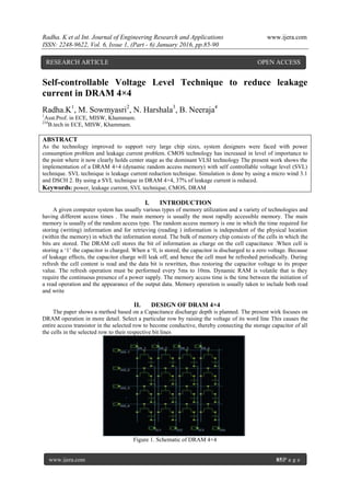
- 1. Radha. K et al Int. Journal of Engineering Research and Applications www.ijera.com ISSN: 2248-9622, Vol. 6, Issue 1, (Part - 6) January 2016, pp.85-90 www.ijera.com 85|P a g e Self-controllable Voltage Level Technique to reduce leakage current in DRAM 4×4 Radha.K1 , M. Sowmyasri2 , N. Harshala3 , B. Neeraja4 1 Asst.Prof. in ECE, MISW, Khammam. 234 B.tech in ECE, MISW, Khammam. ABSTRACT As the technology improved to support very large chip sizes, system designers were faced with power consumption problem and leakage current problem. CMOS technology has increased in level of importance to the point where it now clearly holds center stage as the dominant VLSI technology The present work shows the implementation of a DRAM 4×4 (dynamic random access memory) with self controllable voltage level (SVL) technique. SVL technique is leakage current reduction technique. Simulation is done by using a micro wind 3.1 and DSCH 2. By using a SVL technique in DRAM 4×4, 37% of leakage current is reduced. Keywords: power, leakage current, SVL technique, CMOS, DRAM I. INTRODUCTION A given computer system has usually various types of memory utilization and a variety of technologies and having different access times . The main memory is usually the most rapidly accessible memory. The main memory is usually of the random access type. The random access memory is one in which the time required for storing (writing) information and for retrieving (reading ) information is independent of the physical location (within the memory) in which the information stored. The bulk of memory chip consists of the cells in which the bits are stored. The DRAM cell stores the bit of information as charge on the cell capacitance .When cell is storing a „1‟ the capacitor is charged. When a „0, is stored, the capacitor is discharged to a zero voltage. Because of leakage effects, the capacitor charge will leak off, and hence the cell must be refreshed periodically. During refresh the cell content is read and the data bit is rewritten, thus restoring the capacitor voltage to its proper value. The refresh operation must be performed every 5ms to 10ms. Dynamic RAM is volatile that is they require the continuous presence of a power supply. The memory access time is the time between the initiation of a read operation and the appearance of the output data. Memory operation is usually taken to include both read and write II. DESIGN OF DRAM 4×4 The paper shows a method based on a Capacitance discharge depth is planned. The present wirk focuses on DRAM operation in more detail. Select a particular row by raising the voltage of its word line This causes the entire access transistor in the selected row to become conductive, thereby connecting the storage capacitor of all the cells in the selected row to their respective bit lines Figure 1. Schematic of DRAM 4×4 RESEARCH ARTICLE OPEN ACCESS
- 2. Radha. K et al Int. Journal of Engineering Research and Applications www.ijera.com ISSN: 2248-9622, Vol. 6, Issue 1, (Part - 6) January 2016, pp.85-90 www.ijera.com 86|P a g e Which used a word line 1, 2, 3, 4 as a controlling transistor and bit line 1, 2, 3, 4, as a data information and s1, s2, s3, and s4 as an output lines. Data is access when a word line is high otherwise no written operation is performed. If word line 1 is ON, in that time bit line 1 have some information than s1 output is high and one transistor in the columns is closed compare to other. Similarly to other transistor is in working condition when word line is high with respect to bit line. The Layout of DRAM 4×4 is given in figure 2 which is implemented in microwind 3.1 using a design palette for the design of NMOS, word line, and bit line. The waveform of DRAM 4×4 is shown above. It shows that when a bit line 1 is high in that time first row is activated means gives the information on the bit line. Similarly to bit line 2, bit line 3 , and bit line 4 is high with respect to word line is also high , gives the information which is delivered and write operation is performed. The leakage current responsible for draining the soft-node capacitance over time has two main components, namely, the sub threshold channel current and the reverse conduction current of the drain-substrate junction . The reverse diode leakage occurs when the p n junction between the drain and the bulk of the transistor is reverse-biased. The reverse leakage current of a p n junction is expressed by
- 3. Radha. K et al Int. Journal of Engineering Research and Applications www.ijera.com ISSN: 2248-9622, Vol. 6, Issue 1, (Part - 6) January 2016, pp.85-90 www.ijera.com 87|P a g e Vbias = reverse bias voltage across the junction Js = reverse saturation current density A = junction area Another component of leakage currents in CMOS circuits is the sub threshold current, which is due to carrier diffusion between the source and the drain regions of the transistor in weak inversion. q= electron charge Dn = density for nmos VGS= gate to source voltage VDS = drain to source voltage T = temperature K = Boltzmann‟s constant KT/q = thermal voltage _F = electrical dependent parameter So I leakage = I sub threshold + I reverse The total charge stored in the soft node as the Sum of two main components, as follows. Q = Q j (Vx) + Qin, Where Qin = Cin* Vx. Vx= soft node voltage Cin =input capacitance Cin = Cgb + Cpoly + Cmetal Cgb = gate to bulk capacitance Cpoly= polysilicon capacitance The total leakage current can be expressed as the time derivative of the total soft-node charge Q. The leakage current is shown in figure 4. In this research paper also shows the frequency versus time waveform. Variation of frequency with respect to time gives a different value of frequency in which the data information has met during write capability. The waveform of voltage versus current is shown in figure 5. In the diagram shows a variation of Voltage with respect to current
- 4. Radha. K et al Int. Journal of Engineering Research and Applications www.ijera.com ISSN: 2248-9622, Vol. 6, Issue 1, (Part - 6) January 2016, pp.85-90 www.ijera.com 88|P a g e Now the DRAM 4×4 is implemented with the self controllable voltage level (SVL) technique. By using the self controllable voltage level reduce the leakage current in the DRAM4×4. In the SVL used a NMOS and PMOS that is connected in the bit line and output and controlling by using a world line. Now controlling the leakage current in the circuit the SVL circuit is connected in upper and lower side. The correlation of the map is shown in figure 7 and also shows the layout diagram in figure 8. The layout of any circuit to be manufactured by Using a particular process must confirm to a set of geometric rules which are generally called a layout design rules. These rules usually specify the minimum allowable line width for physical objects on chip such as metal and poly silicon interconnect or diffusion area, minimum feature dimension and minimum allowable separation between two such features. The layout modifications are usually concentrated on the width to length ratio of the transistors (transistorizing). The transistor size is change, the leakage current is affected. Implementation of the DRAM 4×4 with self controllable voltage level reduce the leakage current and output waveform is shown in figure 9. The leakage current reduction shown in figure 10. The leakage current reduces
- 5. Radha. K et al Int. Journal of Engineering Research and Applications www.ijera.com ISSN: 2248-9622, Vol. 6, Issue 1, (Part - 6) January 2016, pp.85-90 www.ijera.com 89|P a g e by using the self controllable voltage level is 37%.Voltage versus current waveform with SVL is also shown in the figure 11. The variation of the frequency versus time shown in figure 12. In this work we presented a DRAM 4×4 with self controllable voltage level. To implement DRAM4×4 with self controllable voltage level gives the advantageous of reduction up to 37%. The layout of Simulation is done by using a microwind 3.1. VDD is used in this 1.2v. Here 0.12μm technology is used. REFERENCES [1.] Frangois Odiot, Hugues Brut, “New Test Structure For High Resozution Leakage Current And Capacitance Measurements In CMOS Imager Appncations,” Proc. 1EEE 2004 Int. Conference On Microelectronic Test Structures, Vol 17, March 2004. [2.] Satoshi Kurihara, Yanuar Z. Arief, Takumi Tsurusaki, Shinya Ohtsuka, “Construction Of Remote Monitoring System For Separative Measurement Of Leakage Current Of Outdoor Insulators,” Proceedings Of The 7th Lntemarional Conference On Properties And Applications Of Dielectric Materials June 1-5 2003 Nagoya.
- 6. Radha. K et al Int. Journal of Engineering Research and Applications www.ijera.com ISSN: 2248-9622, Vol. 6, Issue 1, (Part - 6) January 2016, pp.85-90 www.ijera.com 90|P a g e [3.] Rajeev Rao, Student Member, IEEE, Ashish Srivastava, Student Member, IEEE, David Blaauw, Member, IEEE, And Dennis Sylvester, Member, IEEE, ” Statistical Analysis Of Subthreshold Leakage Current For VLSI Circuits,‟‟ Ieee Transactions On Very Large Scale Integration (Vlsi) Systems, Vol. 12, No. 2, February 2004. [4.] F. Meghnefi, C. Volat And M. Farzaneh, “Temporal And Frequency Analysis Of The Leakage Current Of A Station Post Insulator During Ice Accretion,” IEEE Transactions On Dielectrics And Electrical Insulation Vol. 14, No. 6;December 2007. [5.] Lin Yuan and Gang Qu, “A Combined Gate Replacement and Input Vector Control Approach for Leakage Current Reduction,” Ieee Transactions On Very Large Scale Integration (Vlsi) Systems, Vol. 14, No. 2, February 2006 [6.] Soo Han Choi, Young Hee Park, Chul Hong Park, Sang Hoon Lee, Moon Hyun Yoo1, “Efficient Characterization And Suppression Methodology Of Edge Effects For Leakage Current Reduction Of Sub-40nm DRAM Device,” IEEE International Conference On Microelectronic Test Structures, March 22-25, Hiroshima, Japan 2010. [7.] Dongwoo Lee, Student Member, IEEE, David Blaauw, Member, IEEE, And Dennis Sylvester, Member, IEEE, “Gate Oxide Leakage Current Analysis And Reduction For VLSI Circuits,” IEEE Transactions On Very Large Scale Integration (Vlsi) Systems, Vol. 12, No. 2, February 2004 . [8.] N. H. E. Weste, And K. Eshraghian, Editor. “Principles Of Cmos Vlsi Design”, A Systems Perspective, 2nd Ed. Addison-Wesley, 1993. [9.] Chao-Chi Hong, Chang-Yun Chang, Chaung-Yuan Lee, And Jenn-Gwo Hwu, Senior Member, IEEE, “Reduction In Leakage Current Of Low-Temperature Thin-Gate Oxide By Repeated Spike Oxidation Technique,” IEEE Electron Device Letters, Vol. 23, No. 1, January 2002 [10.] Yutaka Kobayashi, Kyoichiro Asayama, Masayuki Oohayashi, Ryoichi Hori, Goro Kitsukawa, And Kiyoo Itoh, “Bipolar Cmos-Merged Technology For A High-Speed 1 - Mbit Dram,” IEEE Transactions On Electron Devices, Vol. 36, No. 4. April 1989. [11.] Pavan.T.K. Jagannadha Naidu.K Shekar Babu.M,” Implementation Of Delay And Power Monitoring Schemes To Reduce The Power Consumption, Proceedings Of 2011 International Conference On Signal Processing, Communication, Computing And Networking Technologies (ICSCCN 2011). [12.] Mohammad Sharifkhani, Member, IEEE, And Manoj Sachdev, Senior Member, IEEE, “Segmented Virtual Ground Architecture For Low-Power Embedded SRAM, IEEE Transactions On Very Large Scale Integration Systems, Vol. 15, No. 2, February 2007. [13.] Yuh-Fang Tsai, Student, IEEE, David E. Duarte, Member, IEEE, N. Vijaykrishnan, Member, Ieee, And Mary Jane Irwin, Fellow, IEEE, “Characterization And Modeling Of Run- Time Techniques For Leakage Power Reduction,” IEEE Transactions On Very Large Scale Integration (VLSI) Systems, Vol. 12, No. 11, November 2004. [14.] 14.Sung-Mo kang yusef leblebici, Editor. “CMOS Digital Integrated circuit”, Analysis and Design , 3rd Ed. Tata McGraw-hill edition 2003.