SlideShare a Scribd company logo
1 of 8
Download to read offline
International Journal of Electrical and Computer Engineering (IJECE)
Vol. 7, No. 1, February 2017, pp. 144~151
ISSN: 2088-8708, DOI: 10.11591/ijece.v7i1.pp144-151  144
Journal homepage: http://iaesjournal.com/online/index.php/IJECE
Performance Evaluation of GaN Based Thin Film Transistor
using TCAD Simulation
Shashi Kant Dargar, J K Srivastava, Santosh Bharti, Abha Nyati
Department of Electronics and Communication Engineering, Sir Padampat Singhania University, India
Article Info ABSTRACT
Article history:
Received Jul 8, 2016
Revised Oct 26, 2016
Accepted Nov 11, 2017
As reported in past decades, gallium nitride as one of the most capable
compound semiconductor, GaN-based high-electron mobility transistors are
the focus of intense research activities in the area of high power, high-speed,
and high-temperature transistors. In this paper we present a design and
simulation of the GaN based thin film transistor using sentaurus TCAD for
the extracting the electrical performance. The resulting GaN TFTs exhibits
good electrical performance in the simulated results, including, a threshold
voltage of 12-15 V, an on/off current ratio of 6.5×10⁷
~ 8.3×10⁸
, and a sub-
threshold slope of 0.44V/dec. Sentaurus TCAD simulations is the tool which
offers study of comprehensive behavior of semiconductor structures with
ease. The simulation results of the TFT structure based on gallium nitride
active channel have great prospective in the next-generation flat-panel
display applications.
Keyword:
GaN
Mobility
On-off ratio
TCAD
Thin film transistor
Copyright © 2017 Institute of Advanced Engineering and Science.
All rights reserved.
Corresponding Author:
Shashi Kant Dargar,
Department of Electronics and Communication Engineering,
Sir Padampat Singhania University,
FR-4, Flat No. 66 Sir Padampat Singhania University, Bhatewar, Udaipur, India.
Email: shashi.kant@spsu.ac.in
1. INTRODUCTION
A TFT is a special kind of Field effect transistor which is made by depositing thin films of a
semiconductor active layer as well as dielectric layer and metallic contacts over a supporting substrate. A
common substrate is glass, since the primary application of TFTs is in liquid crystal displays (LCD). This
differs from the conventional transistor where substrate is semiconductor material itself, such as a Si wafer.
The basic operation of a TFT is illustrated in Figure 1.
Figure 1. Illustration of TFT Basic Operation
Channel Layer
Insulating Gate
Drain
Contact
Source
Contact
Gate
IJECE ISSN: 2088-8708 
Performance Evaluation of GaN Based Thin Film Transistor Using TCAD Simulation (Shashi Kant Dargar)
145
Hydrogenated amorphous silicon (a-Si:H) is still most popular technology in Thin Film Transistors
(TFTs) for large area electronics such as X-ray imagers, and it is also heavily utilized in photovoltaic
applications. a-Si:H TFTs have low off current and sufficient on/off current ratio for current large area
applications; however, their field effect mobility and stability of threshold voltage. The low mobility limits
not only pixel size but also prohibits complementary circuit implementation using a-Si:H. Since the hole
mobility in a-Si:H is several orders lower than electron mobility, p-type transistor implementation is not
practical which makes designing usable complementary circuit impossible [1]. On the other hand, the drifting
threshold voltage means that a-Si:H TFTs cannot be implemented in column multiplexor and row shift
register circuits [2]. Polycrystalline silicon (Poly-Si) had been proposed to resolve these problems and
replace a-Si:H. However, Poly-Si technology has drawbacks on production side since it requires a large and
expensive laser annealing system.
Over the past several years, the inherent scaling limitations of electron devices have fueled the
exploration of high carrier mobility semiconductors as a Si replacement to further enhance the device
performance. In particular, compound semiconductors heterogeneously integrated on Si substrates have been
actively studied, combining the high mobility of compound semiconductors and the well-established, low
cost processing of Si technology [3].
It can be comprehended that there are three regions of operation. For small gate voltages, the Fermi
level lies in the deep states and it can be assumed that the energy bands are close to flat band condition. With
an increase in the positive gate bias, causes bending near to the gate dielectric interface and this increases
fermi level through the deep states and towards the band tail states [4].
In this state, most of induced electrons are trapped in deep defect states, a small but negligible
amount of electrons may occupy tail states yield a small amount of drain current. This operation region is
called the sub threshold region shown in Figure 1. The sub–threshold region continues until the deep states
are filled up with electrons and the concentration of electrons in tail states exceeds that of trapped electrons in
deep states. As the gate bias continues to increase, it finally exceeds a threshold voltage (Vth) which implies
the Fermi level now lies in the tail states [5-6]. For gate–source bias (Vgs) higher than Vth, the TFT is
operating in the above threshold regime, i.e. ON state.
With the continuous demand in reduction of physical gate lengths of the electronic devices such as
TFTs new device architectures will be required to reach the performance of the future technology
generation [7]. In addition, control of gate leakage current requires the introduction of gate insulators with
high dielectric constants, and the need for increased carrier mobility pushes the use of unconventional
channel materials and processing to induce appropriate stresses. The availability of advanced models and
simulation tools has significant importance to achieve these goals due to following reasons:
1) Early evaluations of the most promising device architectures and materials in terms of performance and
potential for continued scaling.
2) Assessments of processing and design strategies.
3) Reductions of cycle time and of R&D costs. Measurements and tests at the nanoscale tend to be much
more expensive than at the microscale and macroscale [8].
The main aim of this paper is to simulate the thin–film transistor using GaN as an active channel
layer. This involves the generation of the thin film based TFT structures using Sentaurus TCAD software.
Simulations of the same to obtain the electrical characteristics and hence the extraction of electrical
parameters like threshold voltage, mobility and ON/OFF ratio will enable in determining the functioning
characteristics of the device.
2. ELECTRICAL PROPERTIES AND CHARACTERISTICS OF TFT
The uniqueness of the thin film transistor technology lies in the composing materials and structure
with few parameters on the substrate material and size. Vth measured in Volts, Ion/off, field effect mobility in
cm2
/Vs and subthreshold voltage in V/decade are the parameters which conclude the electrical performance
of the device.
2.1. Threshold Voltage
Vth is the gate voltage necessary to turn on the transistor. It should be low so that it takes low voltage
to turn TFT on or off. It is measured in the saturation region i.e. VDS ≥ VGS – VT.
Ids using square law model of TFT can be given by [9]:
( ) ( ) (1)
 ISSN: 2088-8708
IJECE Vol. 7, No. 1, February 2017 : 144 – 151
146
where W, L, CG and μ are the TFT channel width, length, gate capacitance and field-effect mobility
respectively. To measure Vth after square root the equation (1) we get
√ { ( )} (2)
Now by plotting √IDS vs. VGS and by extrapolating down to the x-axis as shown in Figure 2, the
threshold voltage can be determined.
Figure 2. Linear fit on square root of transfer characteristics of a typical TFT, adopted from [5]
2.2. On/Off Current Ratio
Drain current on/off ratio is another measure of the switching behavior of the TFT. It is simply the
ratio between highest measured current (the on-state current, Ion) to the lowest measured current (the off-
state current, Ioff) as shown in Figure. Ioff is also a measure of the gate leakage present in the device.
2.3. Mobilty
The mobility characterizes how quickly an electron can move through a metal or semiconductor,
when pulled by an electric field. Mobility, μ, is defined as a linear proportionality constant relating the
carrier drift velocity, vd, to the applied electric field E. Effective mobility, μEFF, and field-effect mobility,
μFE, are the two commonly used definitions for the assessment of the mobility of carriers in a field effect
transistor. Effective mobility, μEFF, is extracted from the drain conductance, gD, which is dId/dVds measured in
the linear regime of operation. As Field effect mobility, μEFF, is extracted from the transconductance, gm,
which is dId/dVds gm can be known by transfer characteristics. Means VGS ID curve. μFE employed as
estimators of TFT channel mobility.
2.4. Sub Threshold
Another important parameter is subthreshold slope, which characterizes the effectiveness of the Gate
voltage in reducing drain current to zero.
The subthreshold slope can be given by equation (3)
(3)
To achieve high on/off current ratios, subthreshold slopes should be low so that the same difference
in VGS can decrease the drain current by more decades. Depending on the gate-source voltage VGS, different
regions of operation can be identified: above-threshold, subthreshold, and Poole-Frenkel emission.
In the subthreshold region of operation, the TFT switches from off to on and the current changes
exponentially from a low off current, which is in pA, to a high on current, which is in µA.
Forward subthreshold regionis Vth >VGS > 0
IJECE ISSN: 2088-8708 
Performance Evaluation of GaN Based Thin Film Transistor Using TCAD Simulation (Shashi Kant Dargar)
147
The drain current equation (4) in the forward subthreshold region is given by [11]:
(4)
where Isub0 is the magnitude of current in the subthreshold region, and Sf is the forward subthreshold region.
The drain current equation (5) in the reverse subthreshold region is defined by following equation [11]
| |
(5)
where Sr is the reverse subthreshold slope and γn is a unitless parameter accounting for two dimensional
effects.
3. DESIGNING OF STRUCTURE
Semiconductor manufacturers face the challenge of developing process technologies within strict
time and cost constraints. TCAD reduces the number of engineering wafers, saving time and money.
3.1. Generation of TFT Structure using Sentaurus TCAD
Using the Sentaurus Structure Editor the 2D structure of the TFT is drawn. Graphical User interface
of Structure editor opens a window after pressing command line. This window has its three part.The menu
bar, toolbars, and lists are in the upper part of the main window; the view window is in the center; and the
command-line window is in the lower part of the main window. Contacts can be defined to allow the
constructed device to be connected to outside power sources. The contacts name, sets, properties, edge color,
thickness are defined for the specific structure. Figure 3 shows the structure of TFT with with GaN as an
active channel layer which is designed with a 100/50 µm as a W/L.
Figure 3. Structure used for Two Dimensional Simulation of GaN Channel TFT using Sentaurus TCAD
3.2. Defining doping of the TFT Structure using Sentaurus TCAD
A constant boron background doping of 1 x 10¹⁵
cm-3
in the silicon material is introduced by
appropriate selection in the constant profile placement dialog box with placement name, material, species,
and concentration field. The doping profile is chosen with and concentration of 1e+15and arsenic active
concentration are dopants are included by the addition of constant doping profile into the silicon for obtaining
the increased mobility in the dielectric semiconductor interface.
3.3. Defining meshing Strategy of the Structure and Generation of Mesh
After the device is structured, contacts are set and doping profile has been selected. The next step is
called meshing. Sentaurus Mesh is a modular 2D and 3D mesh generator that can create both axis-aligned
and tensor meshes to be used in simulators that use the box discretization or finite-difference time-domain
(FDTD) methods for spatial device discretization. Sentaurus Mesh produces triangles in the case of 2D
devices and tetrahedra in the case of 3D devices. Generated grids can be loaded into Sentaurus Device and
 ISSN: 2088-8708
IJECE Vol. 7, No. 1, February 2017 : 144 – 151
148
Sentaurus Process. Depending on the mesh generator used, Sentaurus Mesh produces different output
formats. The axis-aligned mesh generator always produces a TDR unstructured mesh. In Sentaurus Structure
Editor, the mesh generation process is performed in two steps. The first step defines the meshing strategy,
which includes the maximum and minimum meshing step definition in each device dimensions as well as the
mesh refinement strategies. The second step links the defined strategy from the first step to a specific target,
which is, in general, a material, or a device region, or a user-defined evaluation window. Note that different
device regions have different roles in terms of determining the device performance, thereby the required
meshing strategies for these regions are typically different. Figure 4 and figure 5 shows the meshing strategy
adopted for the min-max element size and build mesh is successfully generated as shown in the Figure 6.
Figure 4. Structure used for two dimensional simulation of bottom gate GaN channel TFT using sentaurus
TCAD
Figure 5. Defining Meshing Strategy and doping profile GaN channel TFT
Figure 6. Defining doping profile build mesh of the structure
IJECE ISSN: 2088-8708 
Performance Evaluation of GaN Based Thin Film Transistor Using TCAD Simulation (Shashi Kant Dargar)
149
4. RESULT AND DISCUSSION
On increasing gate bias the carriers induced in the inversion get trapped in the defect sates and
potential barrier increases in height and the traps become full and the additional carriers then reduces the
depletion width. Therefore, a threshold voltage is required to overcome the potential barrier created due to
defect states and to drive the thin film transistor in ON state. Figure 7 represents the transfer curves of the
simulated structure. Standard FET theory has been used to extract the channel threshold voltage. The
achieved current ON/OFF ratio is quite good because of presence of low defects as compared to the a–si: H.
These values are quite comparable to a–si: H, a–C: H values [12], [13]. The drain current is clearly
modulated by the applied gate bias. For the extraction of electrical paraetrs drain vloatage current
charcaterics are obatined depicted in Figure 8.
Figure 7. Simulated transfer characteristics for different values of drain to source bias
Figure 8. Simulated drain characteristics for different values of gate to source bias
5. CONCLUSION
Design and simulation of the GaN based thin film transistor using sentaurus TCAD is presented in
this paper. This lead to extract and evaluate the electrical performance of thin film transistor. The resulting
GaN TFTs exhibits good electrical performance in the simulated results, including, a threshold voltage of
12-15 V, an on/off current ratio of 6.5×10⁷
~ 8.3×10⁸
, and a sub-threshold slope of 0.44V/dec. All these
values have to be corroborated with experimental values, which is a part of future work. Sentaurus TCAD
simulations is the tool which offers study of comprehensive behavior of semiconductor structures with ease.
The simulation results of the TFT structure based on gallium nitride active channel have great prospective in
the next-generation flat-panel display applications. With further experimentation may be carried for the better
 ISSN: 2088-8708
IJECE Vol. 7, No. 1, February 2017 : 144 – 151
150
approximation to estimate electrical characteristics of the semiconductor device by use of simulation of
similar TFTs by incorporating different structure, doping profile, and variation of materials in regions.
Table 2.Threshold Voltage, ON/OFF Ratio, Saturation Mobility and Sub–Threshold Slope Values under
different DOS Values
Parameter
Density of States
(1x10¹⁵
) in cm-3
eV-1
Density of States
(1x10¹⁸
) in cm-3
eV-1
Threshold Voltage (V) ~ 15 ~ 12
ON current 1.4 × 10⁷
2.5×10⁸
Off current 0.21427 0.31224
ON/OFF ratio 6.5×10⁷
8.3×10⁸
Saturation Mobility 3.36×10⁻⁶
6.97×10⁻³
Sub-threshold
slope(V/decade)
0.44 0.36
ACKNOWLEDGEMENTS
We pay our special thanks for appreciative original work of all the authors of various technical
papers which we have referred in initiation of the work without which it was very difficult to achieve
successful completion. We also wish to put on record the word of appreciation for the developers of tool,
techniques and their easy access to the learner and researchers.
REFERENCES
[1] Y. Kuo, “Thin Film Transistor Technology-Past, Present, and Future,” The Electrochemical Society Interface,
spring, 2013.
[2] I. D. French, et al., “Microcrystalline si TFTs for integrated multiplexers and shift registers,” Proceedings of 21st
International Display Conference and 8th International Display Workshops, Japan, pp. 367, 2001.
[3] H. Ko, et al., “Ultrathin compound semiconductor on insulator layers for high performance nanoscale transistors,”
Nature, vol. 468, pp. 286-289, 2010.
[4] Nanocluster carbon thin film as a semiconducting layer and feasibility for device application
[5] M. J. Powell, “The physics of amorphous-silicon thin-film transistors,” IEEE Transactions on Electron Devices,
vol. 36, pp. 2753-63, 1989.
[6] M. Shur and M. Hack, “Physics of amorphous silicon based alloy field-effect transistors,” Journal of Applied
Physics, vol. 55, pp. 3831-42, 1984.
[7] Dargar S. K. and Srivastava J. K., “Performance of Thin Film Transistor: A Review,” Asia Pacific Journal of
Engineering Science and Technology, vol/issue: 2(3), pp. 1-14, 2016.
[8] “Foreword Special Issue on Simulation and Modeling of Nanoelectronics Devices,” IEEE transactions on electron
devices, vol/issue: 54(9), pp. 2072-78, 2007.
[9] Y. Yamamoto, “Technological Innovation of Thin-Film Transistors: Technology Development, History, and
Future,” Japanese Journal of Applied Physics, vol. 51, 2012.
[10] S. Geissler, et al., “A thermally activated gate current in off-state PMOSFETs,” Reliability Physics Symposium
Annual Proceedings International, pp. 123-128, 1991.
[11] A. A. Orouji and M. J. Kumar, “Leakage Current Reduction Techniques in Poly-Si TFTs for Active Matrix Liquid
Crystal Displays: A Comprehensive Study,” IEEE Transactions on device and materials reliability, vol/issue: 6(2),
2006.
[12] R. Chen, et al., “Bottom-Gate Thin-Film Transistors Based on GaN Active Channel Layer,” IEEE Electron Device
Lett., vol/issue: 34(4), 2013.
BIOGRAPHIES OF AUTHORS
Shashi Kant Dargar is working Assistant Professor in the Department Electronics and
Communication Engineering at Sir Padampat Singhania University, Udaipur. He has completed
his degree of Bachelor of Engineering from University of Rajasthan in specialization with
Electronics and Communication Engineering and M. Tech. in Digital Communication from
Rajasthan Technical University. He is currently pursuing his PhD in thin film transistor design.
He has been contributing in academics from 10 years. His area of research interest is signal
processing, wireless communication, Microwave & Communication Engineering and thin film
transistor.
IJECE ISSN: 2088-8708 
Performance Evaluation of GaN Based Thin Film Transistor Using TCAD Simulation (Shashi Kant Dargar)
151
J.K. Shrivastava is working Assistant Professor in the Department Electronics and
Communication Engineering at Sir Padampat Singhania University, Udaipur. He has completed
his Ph.D. form IIT-BHU from department of Electronics Engineering and have completed M.Sc.
From Dr. R.M.L. (Awadh), University Faizabad in the Electronics Engineering. He did his B.Sc.
from LBS PG College Gonda. His research interest is Thick Film and Thin film gas sensors.
Santosh Kumar Bharti is working Assistant Professor in the Department Electronics and
Communication Engineering at Sir Padampat Singhania University, Udaipur. He has completed
his B.Tech. From UNSIET, Jaunpur VBS purvanchal University in the Electronics Engineering.
He did his M.Tech in Electronics and Communication Engineering specialized in Digital
Communication Engineering from NIT Kurukshtra Haryana (India). He has been Contributing in
academics from 8 years. His research interest in wireless communication, WSN and digital
communications.
Abha Nyati is in the field of academics and research from 5 years and have contributed several
papers on communication, antenna design and signal processing. She has completed her M.Tech
in Digital Communication and B.E. in Electronics and Communication Engineering. She is also
the member of engineering society and journals. She has significantly contributed in the above
work for the mathematical understanding and implementation.

More Related Content

What's hot

Three phase shifter appliance
Three phase shifter applianceThree phase shifter appliance
Three phase shifter applianceAnil Maurya
 
Design of a 90⁰ switched line phase shifter for phased array antennas
Design of a 90⁰ switched line phase shifter for phased array antennasDesign of a 90⁰ switched line phase shifter for phased array antennas
Design of a 90⁰ switched line phase shifter for phased array antennaseSAT Publishing House
 
Negative resistance amplifier circuit using GaAsFET modelled single MESFET
Negative resistance amplifier circuit using GaAsFET modelled single MESFETNegative resistance amplifier circuit using GaAsFET modelled single MESFET
Negative resistance amplifier circuit using GaAsFET modelled single MESFETTELKOMNIKA JOURNAL
 
Off-line Fault Localization Technique on HVDC Submarine Cable via Time-Freque...
Off-line Fault Localization Technique on HVDC Submarine Cable via Time-Freque...Off-line Fault Localization Technique on HVDC Submarine Cable via Time-Freque...
Off-line Fault Localization Technique on HVDC Submarine Cable via Time-Freque...ABHISHEK MALAV
 
Self-controllable Voltage Level Technique to reduce leakage current in DRAM 4×4
Self-controllable Voltage Level Technique to reduce leakage current in DRAM 4×4Self-controllable Voltage Level Technique to reduce leakage current in DRAM 4×4
Self-controllable Voltage Level Technique to reduce leakage current in DRAM 4×4IJERA Editor
 
Geometric and process design of ultra-thin junctionless double gate vertical ...
Geometric and process design of ultra-thin junctionless double gate vertical ...Geometric and process design of ultra-thin junctionless double gate vertical ...
Geometric and process design of ultra-thin junctionless double gate vertical ...IJECEIAES
 
MEMS MICROPHONE INTERFACE
MEMS MICROPHONE INTERFACEMEMS MICROPHONE INTERFACE
MEMS MICROPHONE INTERFACEIJERD Editor
 
Design of a CMOS-based microwave active channelized bandpass filter
Design of a CMOS-based microwave active channelized bandpass filterDesign of a CMOS-based microwave active channelized bandpass filter
Design of a CMOS-based microwave active channelized bandpass filterTELKOMNIKA JOURNAL
 
Pe 2010 25-10-a facts device distributed power flow controller
Pe 2010 25-10-a facts device distributed power flow controllerPe 2010 25-10-a facts device distributed power flow controller
Pe 2010 25-10-a facts device distributed power flow controllerSudeepthg Sudeepth
 
Reconfigurable ultra wideband to narrowband antenna for cognitive radio appli...
Reconfigurable ultra wideband to narrowband antenna for cognitive radio appli...Reconfigurable ultra wideband to narrowband antenna for cognitive radio appli...
Reconfigurable ultra wideband to narrowband antenna for cognitive radio appli...TELKOMNIKA JOURNAL
 
Combined Defence Services Examination (II) - 2014Performance analysis of swcn...
Combined Defence Services Examination (II) - 2014Performance analysis of swcn...Combined Defence Services Examination (II) - 2014Performance analysis of swcn...
Combined Defence Services Examination (II) - 2014Performance analysis of swcn...eSAT Publishing House
 
Ground Bounce Noise Reduction in Vlsi Circuits
Ground Bounce Noise Reduction in Vlsi CircuitsGround Bounce Noise Reduction in Vlsi Circuits
Ground Bounce Noise Reduction in Vlsi CircuitsIJERA Editor
 

What's hot (18)

Three phase shifter appliance
Three phase shifter applianceThree phase shifter appliance
Three phase shifter appliance
 
Design of a 90⁰ switched line phase shifter for phased array antennas
Design of a 90⁰ switched line phase shifter for phased array antennasDesign of a 90⁰ switched line phase shifter for phased array antennas
Design of a 90⁰ switched line phase shifter for phased array antennas
 
Ferrite phase shifter
Ferrite phase shifterFerrite phase shifter
Ferrite phase shifter
 
Negative resistance amplifier circuit using GaAsFET modelled single MESFET
Negative resistance amplifier circuit using GaAsFET modelled single MESFETNegative resistance amplifier circuit using GaAsFET modelled single MESFET
Negative resistance amplifier circuit using GaAsFET modelled single MESFET
 
Seminar report
Seminar reportSeminar report
Seminar report
 
Off-line Fault Localization Technique on HVDC Submarine Cable via Time-Freque...
Off-line Fault Localization Technique on HVDC Submarine Cable via Time-Freque...Off-line Fault Localization Technique on HVDC Submarine Cable via Time-Freque...
Off-line Fault Localization Technique on HVDC Submarine Cable via Time-Freque...
 
C231924
C231924C231924
C231924
 
Overview of Soft-Switching DC-DC Converters
Overview of Soft-Switching DC-DC ConvertersOverview of Soft-Switching DC-DC Converters
Overview of Soft-Switching DC-DC Converters
 
Self-controllable Voltage Level Technique to reduce leakage current in DRAM 4×4
Self-controllable Voltage Level Technique to reduce leakage current in DRAM 4×4Self-controllable Voltage Level Technique to reduce leakage current in DRAM 4×4
Self-controllable Voltage Level Technique to reduce leakage current in DRAM 4×4
 
Geometric and process design of ultra-thin junctionless double gate vertical ...
Geometric and process design of ultra-thin junctionless double gate vertical ...Geometric and process design of ultra-thin junctionless double gate vertical ...
Geometric and process design of ultra-thin junctionless double gate vertical ...
 
MEMS MICROPHONE INTERFACE
MEMS MICROPHONE INTERFACEMEMS MICROPHONE INTERFACE
MEMS MICROPHONE INTERFACE
 
Design of a CMOS-based microwave active channelized bandpass filter
Design of a CMOS-based microwave active channelized bandpass filterDesign of a CMOS-based microwave active channelized bandpass filter
Design of a CMOS-based microwave active channelized bandpass filter
 
20120140506014
2012014050601420120140506014
20120140506014
 
Pe 2010 25-10-a facts device distributed power flow controller
Pe 2010 25-10-a facts device distributed power flow controllerPe 2010 25-10-a facts device distributed power flow controller
Pe 2010 25-10-a facts device distributed power flow controller
 
Improved Fully Differential Low Power Active Filter
Improved Fully Differential Low Power Active FilterImproved Fully Differential Low Power Active Filter
Improved Fully Differential Low Power Active Filter
 
Reconfigurable ultra wideband to narrowband antenna for cognitive radio appli...
Reconfigurable ultra wideband to narrowband antenna for cognitive radio appli...Reconfigurable ultra wideband to narrowband antenna for cognitive radio appli...
Reconfigurable ultra wideband to narrowband antenna for cognitive radio appli...
 
Combined Defence Services Examination (II) - 2014Performance analysis of swcn...
Combined Defence Services Examination (II) - 2014Performance analysis of swcn...Combined Defence Services Examination (II) - 2014Performance analysis of swcn...
Combined Defence Services Examination (II) - 2014Performance analysis of swcn...
 
Ground Bounce Noise Reduction in Vlsi Circuits
Ground Bounce Noise Reduction in Vlsi CircuitsGround Bounce Noise Reduction in Vlsi Circuits
Ground Bounce Noise Reduction in Vlsi Circuits
 

Similar to Performance Evaluation of GaN Based Thin Film Transistor using TCAD Simulation

Analysis of analog and RF behaviors in junctionless double gate vertical MOSFET
Analysis of analog and RF behaviors in junctionless double gate vertical MOSFETAnalysis of analog and RF behaviors in junctionless double gate vertical MOSFET
Analysis of analog and RF behaviors in junctionless double gate vertical MOSFETjournalBEEI
 
Diodo de Tunelamento Ressonante: Teoria de operação e aplicações
Diodo de Tunelamento Ressonante: Teoria de operação e aplicaçõesDiodo de Tunelamento Ressonante: Teoria de operação e aplicações
Diodo de Tunelamento Ressonante: Teoria de operação e aplicaçõesREGIANE APARECIDA RAGI PEREIRA
 
ECE 6030 Device Electronics.docx
ECE 6030 Device Electronics.docxECE 6030 Device Electronics.docx
ECE 6030 Device Electronics.docxwrite31
 
Review on Tunnel Field Effect Transistors (TFET)
Review on Tunnel Field Effect Transistors (TFET)Review on Tunnel Field Effect Transistors (TFET)
Review on Tunnel Field Effect Transistors (TFET)IRJET Journal
 
A new design of a microstrip rectenna at 5.8 GHz for wireless power transmiss...
A new design of a microstrip rectenna at 5.8 GHz for wireless power transmiss...A new design of a microstrip rectenna at 5.8 GHz for wireless power transmiss...
A new design of a microstrip rectenna at 5.8 GHz for wireless power transmiss...IJECEIAES
 
Introduction gadgets have gained a lot of attention.pdf
Introduction gadgets have gained a lot of attention.pdfIntroduction gadgets have gained a lot of attention.pdf
Introduction gadgets have gained a lot of attention.pdfbkbk37
 
55tmtt05-pfeiffer-proof
55tmtt05-pfeiffer-proof55tmtt05-pfeiffer-proof
55tmtt05-pfeiffer-proofDavid Goren
 
DC and RF characteristics of 20 nm gate length InAlAs/InGaAs/InP HEMTs for hi...
DC and RF characteristics of 20 nm gate length InAlAs/InGaAs/InP HEMTs for hi...DC and RF characteristics of 20 nm gate length InAlAs/InGaAs/InP HEMTs for hi...
DC and RF characteristics of 20 nm gate length InAlAs/InGaAs/InP HEMTs for hi...IJECEIAES
 
Sub-Threshold Leakage Current Reduction Techniques In VLSI Circuits -A Survey
Sub-Threshold Leakage Current Reduction Techniques In VLSI Circuits -A SurveySub-Threshold Leakage Current Reduction Techniques In VLSI Circuits -A Survey
Sub-Threshold Leakage Current Reduction Techniques In VLSI Circuits -A SurveyIJERA Editor
 
RBL paper _Design_of_MIGFET_based_junctionless_transistor
RBL paper _Design_of_MIGFET_based_junctionless_transistorRBL paper _Design_of_MIGFET_based_junctionless_transistor
RBL paper _Design_of_MIGFET_based_junctionless_transistorHema N
 
Analysis of pocket double gate tunnel fet for low stand by power logic circuits
Analysis of pocket double gate tunnel fet for low stand by power logic circuitsAnalysis of pocket double gate tunnel fet for low stand by power logic circuits
Analysis of pocket double gate tunnel fet for low stand by power logic circuitsVLSICS Design
 
Electrical characterization of si nanowire GAA-TFET based on dimensions downs...
Electrical characterization of si nanowire GAA-TFET based on dimensions downs...Electrical characterization of si nanowire GAA-TFET based on dimensions downs...
Electrical characterization of si nanowire GAA-TFET based on dimensions downs...IJECEIAES
 
WIRELESS POWER TRANSMISSION Project
WIRELESS POWER TRANSMISSION ProjectWIRELESS POWER TRANSMISSION Project
WIRELESS POWER TRANSMISSION Projectsagnikchoudhury
 
Wireless Power Transfer Project
Wireless Power Transfer  ProjectWireless Power Transfer  Project
Wireless Power Transfer Projectsagnikchoudhury
 
Performance analysis of ultrathin junctionless double gate vertical MOSFETs
Performance analysis of ultrathin junctionless double gate vertical MOSFETsPerformance analysis of ultrathin junctionless double gate vertical MOSFETs
Performance analysis of ultrathin junctionless double gate vertical MOSFETsjournalBEEI
 
Self-controllable Voltage Level Technique to reduce leakage current in DRAM 4×4
Self-controllable Voltage Level Technique to reduce leakage current in DRAM 4×4Self-controllable Voltage Level Technique to reduce leakage current in DRAM 4×4
Self-controllable Voltage Level Technique to reduce leakage current in DRAM 4×4IJERA Editor
 

Similar to Performance Evaluation of GaN Based Thin Film Transistor using TCAD Simulation (20)

Analysis of analog and RF behaviors in junctionless double gate vertical MOSFET
Analysis of analog and RF behaviors in junctionless double gate vertical MOSFETAnalysis of analog and RF behaviors in junctionless double gate vertical MOSFET
Analysis of analog and RF behaviors in junctionless double gate vertical MOSFET
 
Ijetcas14 647
Ijetcas14 647Ijetcas14 647
Ijetcas14 647
 
Diodo de Tunelamento Ressonante: Teoria de operação e aplicações
Diodo de Tunelamento Ressonante: Teoria de operação e aplicaçõesDiodo de Tunelamento Ressonante: Teoria de operação e aplicações
Diodo de Tunelamento Ressonante: Teoria de operação e aplicações
 
J3602072079
J3602072079J3602072079
J3602072079
 
ECE 6030 Device Electronics.docx
ECE 6030 Device Electronics.docxECE 6030 Device Electronics.docx
ECE 6030 Device Electronics.docx
 
40520130101001
4052013010100140520130101001
40520130101001
 
Review on Tunnel Field Effect Transistors (TFET)
Review on Tunnel Field Effect Transistors (TFET)Review on Tunnel Field Effect Transistors (TFET)
Review on Tunnel Field Effect Transistors (TFET)
 
A new design of a microstrip rectenna at 5.8 GHz for wireless power transmiss...
A new design of a microstrip rectenna at 5.8 GHz for wireless power transmiss...A new design of a microstrip rectenna at 5.8 GHz for wireless power transmiss...
A new design of a microstrip rectenna at 5.8 GHz for wireless power transmiss...
 
Introduction gadgets have gained a lot of attention.pdf
Introduction gadgets have gained a lot of attention.pdfIntroduction gadgets have gained a lot of attention.pdf
Introduction gadgets have gained a lot of attention.pdf
 
55tmtt05-pfeiffer-proof
55tmtt05-pfeiffer-proof55tmtt05-pfeiffer-proof
55tmtt05-pfeiffer-proof
 
DC and RF characteristics of 20 nm gate length InAlAs/InGaAs/InP HEMTs for hi...
DC and RF characteristics of 20 nm gate length InAlAs/InGaAs/InP HEMTs for hi...DC and RF characteristics of 20 nm gate length InAlAs/InGaAs/InP HEMTs for hi...
DC and RF characteristics of 20 nm gate length InAlAs/InGaAs/InP HEMTs for hi...
 
Sub-Threshold Leakage Current Reduction Techniques In VLSI Circuits -A Survey
Sub-Threshold Leakage Current Reduction Techniques In VLSI Circuits -A SurveySub-Threshold Leakage Current Reduction Techniques In VLSI Circuits -A Survey
Sub-Threshold Leakage Current Reduction Techniques In VLSI Circuits -A Survey
 
RBL paper _Design_of_MIGFET_based_junctionless_transistor
RBL paper _Design_of_MIGFET_based_junctionless_transistorRBL paper _Design_of_MIGFET_based_junctionless_transistor
RBL paper _Design_of_MIGFET_based_junctionless_transistor
 
Analysis of pocket double gate tunnel fet for low stand by power logic circuits
Analysis of pocket double gate tunnel fet for low stand by power logic circuitsAnalysis of pocket double gate tunnel fet for low stand by power logic circuits
Analysis of pocket double gate tunnel fet for low stand by power logic circuits
 
Electrical characterization of si nanowire GAA-TFET based on dimensions downs...
Electrical characterization of si nanowire GAA-TFET based on dimensions downs...Electrical characterization of si nanowire GAA-TFET based on dimensions downs...
Electrical characterization of si nanowire GAA-TFET based on dimensions downs...
 
WIRELESS POWER TRANSMISSION Project
WIRELESS POWER TRANSMISSION ProjectWIRELESS POWER TRANSMISSION Project
WIRELESS POWER TRANSMISSION Project
 
Wireless Power Transfer Project
Wireless Power Transfer  ProjectWireless Power Transfer  Project
Wireless Power Transfer Project
 
Performance analysis of ultrathin junctionless double gate vertical MOSFETs
Performance analysis of ultrathin junctionless double gate vertical MOSFETsPerformance analysis of ultrathin junctionless double gate vertical MOSFETs
Performance analysis of ultrathin junctionless double gate vertical MOSFETs
 
Kg3418451855
Kg3418451855Kg3418451855
Kg3418451855
 
Self-controllable Voltage Level Technique to reduce leakage current in DRAM 4×4
Self-controllable Voltage Level Technique to reduce leakage current in DRAM 4×4Self-controllable Voltage Level Technique to reduce leakage current in DRAM 4×4
Self-controllable Voltage Level Technique to reduce leakage current in DRAM 4×4
 

More from IJECEIAES

Cloud service ranking with an integration of k-means algorithm and decision-m...
Cloud service ranking with an integration of k-means algorithm and decision-m...Cloud service ranking with an integration of k-means algorithm and decision-m...
Cloud service ranking with an integration of k-means algorithm and decision-m...IJECEIAES
 
Prediction of the risk of developing heart disease using logistic regression
Prediction of the risk of developing heart disease using logistic regressionPrediction of the risk of developing heart disease using logistic regression
Prediction of the risk of developing heart disease using logistic regressionIJECEIAES
 
Predictive analysis of terrorist activities in Thailand's Southern provinces:...
Predictive analysis of terrorist activities in Thailand's Southern provinces:...Predictive analysis of terrorist activities in Thailand's Southern provinces:...
Predictive analysis of terrorist activities in Thailand's Southern provinces:...IJECEIAES
 
Optimal model of vehicular ad-hoc network assisted by unmanned aerial vehicl...
Optimal model of vehicular ad-hoc network assisted by  unmanned aerial vehicl...Optimal model of vehicular ad-hoc network assisted by  unmanned aerial vehicl...
Optimal model of vehicular ad-hoc network assisted by unmanned aerial vehicl...IJECEIAES
 
Improving cyberbullying detection through multi-level machine learning
Improving cyberbullying detection through multi-level machine learningImproving cyberbullying detection through multi-level machine learning
Improving cyberbullying detection through multi-level machine learningIJECEIAES
 
Comparison of time series temperature prediction with autoregressive integrat...
Comparison of time series temperature prediction with autoregressive integrat...Comparison of time series temperature prediction with autoregressive integrat...
Comparison of time series temperature prediction with autoregressive integrat...IJECEIAES
 
Strengthening data integrity in academic document recording with blockchain a...
Strengthening data integrity in academic document recording with blockchain a...Strengthening data integrity in academic document recording with blockchain a...
Strengthening data integrity in academic document recording with blockchain a...IJECEIAES
 
Design of storage benchmark kit framework for supporting the file storage ret...
Design of storage benchmark kit framework for supporting the file storage ret...Design of storage benchmark kit framework for supporting the file storage ret...
Design of storage benchmark kit framework for supporting the file storage ret...IJECEIAES
 
Detection of diseases in rice leaf using convolutional neural network with tr...
Detection of diseases in rice leaf using convolutional neural network with tr...Detection of diseases in rice leaf using convolutional neural network with tr...
Detection of diseases in rice leaf using convolutional neural network with tr...IJECEIAES
 
A systematic review of in-memory database over multi-tenancy
A systematic review of in-memory database over multi-tenancyA systematic review of in-memory database over multi-tenancy
A systematic review of in-memory database over multi-tenancyIJECEIAES
 
Agriculture crop yield prediction using inertia based cat swarm optimization
Agriculture crop yield prediction using inertia based cat swarm optimizationAgriculture crop yield prediction using inertia based cat swarm optimization
Agriculture crop yield prediction using inertia based cat swarm optimizationIJECEIAES
 
Three layer hybrid learning to improve intrusion detection system performance
Three layer hybrid learning to improve intrusion detection system performanceThree layer hybrid learning to improve intrusion detection system performance
Three layer hybrid learning to improve intrusion detection system performanceIJECEIAES
 
Non-binary codes approach on the performance of short-packet full-duplex tran...
Non-binary codes approach on the performance of short-packet full-duplex tran...Non-binary codes approach on the performance of short-packet full-duplex tran...
Non-binary codes approach on the performance of short-packet full-duplex tran...IJECEIAES
 
Improved design and performance of the global rectenna system for wireless po...
Improved design and performance of the global rectenna system for wireless po...Improved design and performance of the global rectenna system for wireless po...
Improved design and performance of the global rectenna system for wireless po...IJECEIAES
 
Advanced hybrid algorithms for precise multipath channel estimation in next-g...
Advanced hybrid algorithms for precise multipath channel estimation in next-g...Advanced hybrid algorithms for precise multipath channel estimation in next-g...
Advanced hybrid algorithms for precise multipath channel estimation in next-g...IJECEIAES
 
Performance analysis of 2D optical code division multiple access through unde...
Performance analysis of 2D optical code division multiple access through unde...Performance analysis of 2D optical code division multiple access through unde...
Performance analysis of 2D optical code division multiple access through unde...IJECEIAES
 
On performance analysis of non-orthogonal multiple access downlink for cellul...
On performance analysis of non-orthogonal multiple access downlink for cellul...On performance analysis of non-orthogonal multiple access downlink for cellul...
On performance analysis of non-orthogonal multiple access downlink for cellul...IJECEIAES
 
Phase delay through slot-line beam switching microstrip patch array antenna d...
Phase delay through slot-line beam switching microstrip patch array antenna d...Phase delay through slot-line beam switching microstrip patch array antenna d...
Phase delay through slot-line beam switching microstrip patch array antenna d...IJECEIAES
 
A simple feed orthogonal excitation X-band dual circular polarized microstrip...
A simple feed orthogonal excitation X-band dual circular polarized microstrip...A simple feed orthogonal excitation X-band dual circular polarized microstrip...
A simple feed orthogonal excitation X-band dual circular polarized microstrip...IJECEIAES
 
A taxonomy on power optimization techniques for fifthgeneration heterogenous ...
A taxonomy on power optimization techniques for fifthgeneration heterogenous ...A taxonomy on power optimization techniques for fifthgeneration heterogenous ...
A taxonomy on power optimization techniques for fifthgeneration heterogenous ...IJECEIAES
 

More from IJECEIAES (20)

Cloud service ranking with an integration of k-means algorithm and decision-m...
Cloud service ranking with an integration of k-means algorithm and decision-m...Cloud service ranking with an integration of k-means algorithm and decision-m...
Cloud service ranking with an integration of k-means algorithm and decision-m...
 
Prediction of the risk of developing heart disease using logistic regression
Prediction of the risk of developing heart disease using logistic regressionPrediction of the risk of developing heart disease using logistic regression
Prediction of the risk of developing heart disease using logistic regression
 
Predictive analysis of terrorist activities in Thailand's Southern provinces:...
Predictive analysis of terrorist activities in Thailand's Southern provinces:...Predictive analysis of terrorist activities in Thailand's Southern provinces:...
Predictive analysis of terrorist activities in Thailand's Southern provinces:...
 
Optimal model of vehicular ad-hoc network assisted by unmanned aerial vehicl...
Optimal model of vehicular ad-hoc network assisted by  unmanned aerial vehicl...Optimal model of vehicular ad-hoc network assisted by  unmanned aerial vehicl...
Optimal model of vehicular ad-hoc network assisted by unmanned aerial vehicl...
 
Improving cyberbullying detection through multi-level machine learning
Improving cyberbullying detection through multi-level machine learningImproving cyberbullying detection through multi-level machine learning
Improving cyberbullying detection through multi-level machine learning
 
Comparison of time series temperature prediction with autoregressive integrat...
Comparison of time series temperature prediction with autoregressive integrat...Comparison of time series temperature prediction with autoregressive integrat...
Comparison of time series temperature prediction with autoregressive integrat...
 
Strengthening data integrity in academic document recording with blockchain a...
Strengthening data integrity in academic document recording with blockchain a...Strengthening data integrity in academic document recording with blockchain a...
Strengthening data integrity in academic document recording with blockchain a...
 
Design of storage benchmark kit framework for supporting the file storage ret...
Design of storage benchmark kit framework for supporting the file storage ret...Design of storage benchmark kit framework for supporting the file storage ret...
Design of storage benchmark kit framework for supporting the file storage ret...
 
Detection of diseases in rice leaf using convolutional neural network with tr...
Detection of diseases in rice leaf using convolutional neural network with tr...Detection of diseases in rice leaf using convolutional neural network with tr...
Detection of diseases in rice leaf using convolutional neural network with tr...
 
A systematic review of in-memory database over multi-tenancy
A systematic review of in-memory database over multi-tenancyA systematic review of in-memory database over multi-tenancy
A systematic review of in-memory database over multi-tenancy
 
Agriculture crop yield prediction using inertia based cat swarm optimization
Agriculture crop yield prediction using inertia based cat swarm optimizationAgriculture crop yield prediction using inertia based cat swarm optimization
Agriculture crop yield prediction using inertia based cat swarm optimization
 
Three layer hybrid learning to improve intrusion detection system performance
Three layer hybrid learning to improve intrusion detection system performanceThree layer hybrid learning to improve intrusion detection system performance
Three layer hybrid learning to improve intrusion detection system performance
 
Non-binary codes approach on the performance of short-packet full-duplex tran...
Non-binary codes approach on the performance of short-packet full-duplex tran...Non-binary codes approach on the performance of short-packet full-duplex tran...
Non-binary codes approach on the performance of short-packet full-duplex tran...
 
Improved design and performance of the global rectenna system for wireless po...
Improved design and performance of the global rectenna system for wireless po...Improved design and performance of the global rectenna system for wireless po...
Improved design and performance of the global rectenna system for wireless po...
 
Advanced hybrid algorithms for precise multipath channel estimation in next-g...
Advanced hybrid algorithms for precise multipath channel estimation in next-g...Advanced hybrid algorithms for precise multipath channel estimation in next-g...
Advanced hybrid algorithms for precise multipath channel estimation in next-g...
 
Performance analysis of 2D optical code division multiple access through unde...
Performance analysis of 2D optical code division multiple access through unde...Performance analysis of 2D optical code division multiple access through unde...
Performance analysis of 2D optical code division multiple access through unde...
 
On performance analysis of non-orthogonal multiple access downlink for cellul...
On performance analysis of non-orthogonal multiple access downlink for cellul...On performance analysis of non-orthogonal multiple access downlink for cellul...
On performance analysis of non-orthogonal multiple access downlink for cellul...
 
Phase delay through slot-line beam switching microstrip patch array antenna d...
Phase delay through slot-line beam switching microstrip patch array antenna d...Phase delay through slot-line beam switching microstrip patch array antenna d...
Phase delay through slot-line beam switching microstrip patch array antenna d...
 
A simple feed orthogonal excitation X-band dual circular polarized microstrip...
A simple feed orthogonal excitation X-band dual circular polarized microstrip...A simple feed orthogonal excitation X-band dual circular polarized microstrip...
A simple feed orthogonal excitation X-band dual circular polarized microstrip...
 
A taxonomy on power optimization techniques for fifthgeneration heterogenous ...
A taxonomy on power optimization techniques for fifthgeneration heterogenous ...A taxonomy on power optimization techniques for fifthgeneration heterogenous ...
A taxonomy on power optimization techniques for fifthgeneration heterogenous ...
 

Recently uploaded

UNIT - IV - Air Compressors and its Performance
UNIT - IV - Air Compressors and its PerformanceUNIT - IV - Air Compressors and its Performance
UNIT - IV - Air Compressors and its Performancesivaprakash250
 
SPICE PARK APR2024 ( 6,793 SPICE Models )
SPICE PARK APR2024 ( 6,793 SPICE Models )SPICE PARK APR2024 ( 6,793 SPICE Models )
SPICE PARK APR2024 ( 6,793 SPICE Models )Tsuyoshi Horigome
 
Introduction to IEEE STANDARDS and its different types.pptx
Introduction to IEEE STANDARDS and its different types.pptxIntroduction to IEEE STANDARDS and its different types.pptx
Introduction to IEEE STANDARDS and its different types.pptxupamatechverse
 
MANUFACTURING PROCESS-II UNIT-5 NC MACHINE TOOLS
MANUFACTURING PROCESS-II UNIT-5 NC MACHINE TOOLSMANUFACTURING PROCESS-II UNIT-5 NC MACHINE TOOLS
MANUFACTURING PROCESS-II UNIT-5 NC MACHINE TOOLSSIVASHANKAR N
 
(MEERA) Dapodi Call Girls Just Call 7001035870 [ Cash on Delivery ] Pune Escorts
(MEERA) Dapodi Call Girls Just Call 7001035870 [ Cash on Delivery ] Pune Escorts(MEERA) Dapodi Call Girls Just Call 7001035870 [ Cash on Delivery ] Pune Escorts
(MEERA) Dapodi Call Girls Just Call 7001035870 [ Cash on Delivery ] Pune Escortsranjana rawat
 
Introduction to Multiple Access Protocol.pptx
Introduction to Multiple Access Protocol.pptxIntroduction to Multiple Access Protocol.pptx
Introduction to Multiple Access Protocol.pptxupamatechverse
 
Call Girls Service Nagpur Tanvi Call 7001035870 Meet With Nagpur Escorts
Call Girls Service Nagpur Tanvi Call 7001035870 Meet With Nagpur EscortsCall Girls Service Nagpur Tanvi Call 7001035870 Meet With Nagpur Escorts
Call Girls Service Nagpur Tanvi Call 7001035870 Meet With Nagpur EscortsCall Girls in Nagpur High Profile
 
Introduction and different types of Ethernet.pptx
Introduction and different types of Ethernet.pptxIntroduction and different types of Ethernet.pptx
Introduction and different types of Ethernet.pptxupamatechverse
 
Call Girls Pimpri Chinchwad Call Me 7737669865 Budget Friendly No Advance Boo...
Call Girls Pimpri Chinchwad Call Me 7737669865 Budget Friendly No Advance Boo...Call Girls Pimpri Chinchwad Call Me 7737669865 Budget Friendly No Advance Boo...
Call Girls Pimpri Chinchwad Call Me 7737669865 Budget Friendly No Advance Boo...roncy bisnoi
 
The Most Attractive Pune Call Girls Budhwar Peth 8250192130 Will You Miss Thi...
The Most Attractive Pune Call Girls Budhwar Peth 8250192130 Will You Miss Thi...The Most Attractive Pune Call Girls Budhwar Peth 8250192130 Will You Miss Thi...
The Most Attractive Pune Call Girls Budhwar Peth 8250192130 Will You Miss Thi...ranjana rawat
 
CCS335 _ Neural Networks and Deep Learning Laboratory_Lab Complete Record
CCS335 _ Neural Networks and Deep Learning Laboratory_Lab Complete RecordCCS335 _ Neural Networks and Deep Learning Laboratory_Lab Complete Record
CCS335 _ Neural Networks and Deep Learning Laboratory_Lab Complete RecordAsst.prof M.Gokilavani
 
MANUFACTURING PROCESS-II UNIT-2 LATHE MACHINE
MANUFACTURING PROCESS-II UNIT-2 LATHE MACHINEMANUFACTURING PROCESS-II UNIT-2 LATHE MACHINE
MANUFACTURING PROCESS-II UNIT-2 LATHE MACHINESIVASHANKAR N
 
UNIT-III FMM. DIMENSIONAL ANALYSIS
UNIT-III FMM.        DIMENSIONAL ANALYSISUNIT-III FMM.        DIMENSIONAL ANALYSIS
UNIT-III FMM. DIMENSIONAL ANALYSISrknatarajan
 
(RIA) Call Girls Bhosari ( 7001035870 ) HI-Fi Pune Escorts Service
(RIA) Call Girls Bhosari ( 7001035870 ) HI-Fi Pune Escorts Service(RIA) Call Girls Bhosari ( 7001035870 ) HI-Fi Pune Escorts Service
(RIA) Call Girls Bhosari ( 7001035870 ) HI-Fi Pune Escorts Serviceranjana rawat
 
UNIT-II FMM-Flow Through Circular Conduits
UNIT-II FMM-Flow Through Circular ConduitsUNIT-II FMM-Flow Through Circular Conduits
UNIT-II FMM-Flow Through Circular Conduitsrknatarajan
 
The Most Attractive Pune Call Girls Manchar 8250192130 Will You Miss This Cha...
The Most Attractive Pune Call Girls Manchar 8250192130 Will You Miss This Cha...The Most Attractive Pune Call Girls Manchar 8250192130 Will You Miss This Cha...
The Most Attractive Pune Call Girls Manchar 8250192130 Will You Miss This Cha...ranjana rawat
 
Structural Analysis and Design of Foundations: A Comprehensive Handbook for S...
Structural Analysis and Design of Foundations: A Comprehensive Handbook for S...Structural Analysis and Design of Foundations: A Comprehensive Handbook for S...
Structural Analysis and Design of Foundations: A Comprehensive Handbook for S...Dr.Costas Sachpazis
 
Microscopic Analysis of Ceramic Materials.pptx
Microscopic Analysis of Ceramic Materials.pptxMicroscopic Analysis of Ceramic Materials.pptx
Microscopic Analysis of Ceramic Materials.pptxpurnimasatapathy1234
 
VIP Call Girls Service Hitech City Hyderabad Call +91-8250192130
VIP Call Girls Service Hitech City Hyderabad Call +91-8250192130VIP Call Girls Service Hitech City Hyderabad Call +91-8250192130
VIP Call Girls Service Hitech City Hyderabad Call +91-8250192130Suhani Kapoor
 

Recently uploaded (20)

UNIT - IV - Air Compressors and its Performance
UNIT - IV - Air Compressors and its PerformanceUNIT - IV - Air Compressors and its Performance
UNIT - IV - Air Compressors and its Performance
 
SPICE PARK APR2024 ( 6,793 SPICE Models )
SPICE PARK APR2024 ( 6,793 SPICE Models )SPICE PARK APR2024 ( 6,793 SPICE Models )
SPICE PARK APR2024 ( 6,793 SPICE Models )
 
Introduction to IEEE STANDARDS and its different types.pptx
Introduction to IEEE STANDARDS and its different types.pptxIntroduction to IEEE STANDARDS and its different types.pptx
Introduction to IEEE STANDARDS and its different types.pptx
 
MANUFACTURING PROCESS-II UNIT-5 NC MACHINE TOOLS
MANUFACTURING PROCESS-II UNIT-5 NC MACHINE TOOLSMANUFACTURING PROCESS-II UNIT-5 NC MACHINE TOOLS
MANUFACTURING PROCESS-II UNIT-5 NC MACHINE TOOLS
 
(MEERA) Dapodi Call Girls Just Call 7001035870 [ Cash on Delivery ] Pune Escorts
(MEERA) Dapodi Call Girls Just Call 7001035870 [ Cash on Delivery ] Pune Escorts(MEERA) Dapodi Call Girls Just Call 7001035870 [ Cash on Delivery ] Pune Escorts
(MEERA) Dapodi Call Girls Just Call 7001035870 [ Cash on Delivery ] Pune Escorts
 
Introduction to Multiple Access Protocol.pptx
Introduction to Multiple Access Protocol.pptxIntroduction to Multiple Access Protocol.pptx
Introduction to Multiple Access Protocol.pptx
 
Call Girls Service Nagpur Tanvi Call 7001035870 Meet With Nagpur Escorts
Call Girls Service Nagpur Tanvi Call 7001035870 Meet With Nagpur EscortsCall Girls Service Nagpur Tanvi Call 7001035870 Meet With Nagpur Escorts
Call Girls Service Nagpur Tanvi Call 7001035870 Meet With Nagpur Escorts
 
Introduction and different types of Ethernet.pptx
Introduction and different types of Ethernet.pptxIntroduction and different types of Ethernet.pptx
Introduction and different types of Ethernet.pptx
 
Call Girls Pimpri Chinchwad Call Me 7737669865 Budget Friendly No Advance Boo...
Call Girls Pimpri Chinchwad Call Me 7737669865 Budget Friendly No Advance Boo...Call Girls Pimpri Chinchwad Call Me 7737669865 Budget Friendly No Advance Boo...
Call Girls Pimpri Chinchwad Call Me 7737669865 Budget Friendly No Advance Boo...
 
The Most Attractive Pune Call Girls Budhwar Peth 8250192130 Will You Miss Thi...
The Most Attractive Pune Call Girls Budhwar Peth 8250192130 Will You Miss Thi...The Most Attractive Pune Call Girls Budhwar Peth 8250192130 Will You Miss Thi...
The Most Attractive Pune Call Girls Budhwar Peth 8250192130 Will You Miss Thi...
 
CCS335 _ Neural Networks and Deep Learning Laboratory_Lab Complete Record
CCS335 _ Neural Networks and Deep Learning Laboratory_Lab Complete RecordCCS335 _ Neural Networks and Deep Learning Laboratory_Lab Complete Record
CCS335 _ Neural Networks and Deep Learning Laboratory_Lab Complete Record
 
MANUFACTURING PROCESS-II UNIT-2 LATHE MACHINE
MANUFACTURING PROCESS-II UNIT-2 LATHE MACHINEMANUFACTURING PROCESS-II UNIT-2 LATHE MACHINE
MANUFACTURING PROCESS-II UNIT-2 LATHE MACHINE
 
UNIT-III FMM. DIMENSIONAL ANALYSIS
UNIT-III FMM.        DIMENSIONAL ANALYSISUNIT-III FMM.        DIMENSIONAL ANALYSIS
UNIT-III FMM. DIMENSIONAL ANALYSIS
 
(RIA) Call Girls Bhosari ( 7001035870 ) HI-Fi Pune Escorts Service
(RIA) Call Girls Bhosari ( 7001035870 ) HI-Fi Pune Escorts Service(RIA) Call Girls Bhosari ( 7001035870 ) HI-Fi Pune Escorts Service
(RIA) Call Girls Bhosari ( 7001035870 ) HI-Fi Pune Escorts Service
 
UNIT-II FMM-Flow Through Circular Conduits
UNIT-II FMM-Flow Through Circular ConduitsUNIT-II FMM-Flow Through Circular Conduits
UNIT-II FMM-Flow Through Circular Conduits
 
The Most Attractive Pune Call Girls Manchar 8250192130 Will You Miss This Cha...
The Most Attractive Pune Call Girls Manchar 8250192130 Will You Miss This Cha...The Most Attractive Pune Call Girls Manchar 8250192130 Will You Miss This Cha...
The Most Attractive Pune Call Girls Manchar 8250192130 Will You Miss This Cha...
 
Structural Analysis and Design of Foundations: A Comprehensive Handbook for S...
Structural Analysis and Design of Foundations: A Comprehensive Handbook for S...Structural Analysis and Design of Foundations: A Comprehensive Handbook for S...
Structural Analysis and Design of Foundations: A Comprehensive Handbook for S...
 
Roadmap to Membership of RICS - Pathways and Routes
Roadmap to Membership of RICS - Pathways and RoutesRoadmap to Membership of RICS - Pathways and Routes
Roadmap to Membership of RICS - Pathways and Routes
 
Microscopic Analysis of Ceramic Materials.pptx
Microscopic Analysis of Ceramic Materials.pptxMicroscopic Analysis of Ceramic Materials.pptx
Microscopic Analysis of Ceramic Materials.pptx
 
VIP Call Girls Service Hitech City Hyderabad Call +91-8250192130
VIP Call Girls Service Hitech City Hyderabad Call +91-8250192130VIP Call Girls Service Hitech City Hyderabad Call +91-8250192130
VIP Call Girls Service Hitech City Hyderabad Call +91-8250192130
 

Performance Evaluation of GaN Based Thin Film Transistor using TCAD Simulation

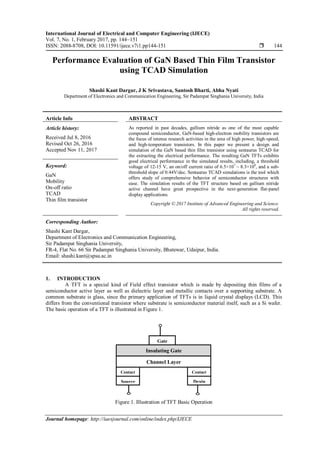
  • 1. International Journal of Electrical and Computer Engineering (IJECE) Vol. 7, No. 1, February 2017, pp. 144~151 ISSN: 2088-8708, DOI: 10.11591/ijece.v7i1.pp144-151  144 Journal homepage: http://iaesjournal.com/online/index.php/IJECE Performance Evaluation of GaN Based Thin Film Transistor using TCAD Simulation Shashi Kant Dargar, J K Srivastava, Santosh Bharti, Abha Nyati Department of Electronics and Communication Engineering, Sir Padampat Singhania University, India Article Info ABSTRACT Article history: Received Jul 8, 2016 Revised Oct 26, 2016 Accepted Nov 11, 2017 As reported in past decades, gallium nitride as one of the most capable compound semiconductor, GaN-based high-electron mobility transistors are the focus of intense research activities in the area of high power, high-speed, and high-temperature transistors. In this paper we present a design and simulation of the GaN based thin film transistor using sentaurus TCAD for the extracting the electrical performance. The resulting GaN TFTs exhibits good electrical performance in the simulated results, including, a threshold voltage of 12-15 V, an on/off current ratio of 6.5×10⁷ ~ 8.3×10⁸ , and a sub- threshold slope of 0.44V/dec. Sentaurus TCAD simulations is the tool which offers study of comprehensive behavior of semiconductor structures with ease. The simulation results of the TFT structure based on gallium nitride active channel have great prospective in the next-generation flat-panel display applications. Keyword: GaN Mobility On-off ratio TCAD Thin film transistor Copyright © 2017 Institute of Advanced Engineering and Science. All rights reserved. Corresponding Author: Shashi Kant Dargar, Department of Electronics and Communication Engineering, Sir Padampat Singhania University, FR-4, Flat No. 66 Sir Padampat Singhania University, Bhatewar, Udaipur, India. Email: shashi.kant@spsu.ac.in 1. INTRODUCTION A TFT is a special kind of Field effect transistor which is made by depositing thin films of a semiconductor active layer as well as dielectric layer and metallic contacts over a supporting substrate. A common substrate is glass, since the primary application of TFTs is in liquid crystal displays (LCD). This differs from the conventional transistor where substrate is semiconductor material itself, such as a Si wafer. The basic operation of a TFT is illustrated in Figure 1. Figure 1. Illustration of TFT Basic Operation Channel Layer Insulating Gate Drain Contact Source Contact Gate
  • 2. IJECE ISSN: 2088-8708  Performance Evaluation of GaN Based Thin Film Transistor Using TCAD Simulation (Shashi Kant Dargar) 145 Hydrogenated amorphous silicon (a-Si:H) is still most popular technology in Thin Film Transistors (TFTs) for large area electronics such as X-ray imagers, and it is also heavily utilized in photovoltaic applications. a-Si:H TFTs have low off current and sufficient on/off current ratio for current large area applications; however, their field effect mobility and stability of threshold voltage. The low mobility limits not only pixel size but also prohibits complementary circuit implementation using a-Si:H. Since the hole mobility in a-Si:H is several orders lower than electron mobility, p-type transistor implementation is not practical which makes designing usable complementary circuit impossible [1]. On the other hand, the drifting threshold voltage means that a-Si:H TFTs cannot be implemented in column multiplexor and row shift register circuits [2]. Polycrystalline silicon (Poly-Si) had been proposed to resolve these problems and replace a-Si:H. However, Poly-Si technology has drawbacks on production side since it requires a large and expensive laser annealing system. Over the past several years, the inherent scaling limitations of electron devices have fueled the exploration of high carrier mobility semiconductors as a Si replacement to further enhance the device performance. In particular, compound semiconductors heterogeneously integrated on Si substrates have been actively studied, combining the high mobility of compound semiconductors and the well-established, low cost processing of Si technology [3]. It can be comprehended that there are three regions of operation. For small gate voltages, the Fermi level lies in the deep states and it can be assumed that the energy bands are close to flat band condition. With an increase in the positive gate bias, causes bending near to the gate dielectric interface and this increases fermi level through the deep states and towards the band tail states [4]. In this state, most of induced electrons are trapped in deep defect states, a small but negligible amount of electrons may occupy tail states yield a small amount of drain current. This operation region is called the sub threshold region shown in Figure 1. The sub–threshold region continues until the deep states are filled up with electrons and the concentration of electrons in tail states exceeds that of trapped electrons in deep states. As the gate bias continues to increase, it finally exceeds a threshold voltage (Vth) which implies the Fermi level now lies in the tail states [5-6]. For gate–source bias (Vgs) higher than Vth, the TFT is operating in the above threshold regime, i.e. ON state. With the continuous demand in reduction of physical gate lengths of the electronic devices such as TFTs new device architectures will be required to reach the performance of the future technology generation [7]. In addition, control of gate leakage current requires the introduction of gate insulators with high dielectric constants, and the need for increased carrier mobility pushes the use of unconventional channel materials and processing to induce appropriate stresses. The availability of advanced models and simulation tools has significant importance to achieve these goals due to following reasons: 1) Early evaluations of the most promising device architectures and materials in terms of performance and potential for continued scaling. 2) Assessments of processing and design strategies. 3) Reductions of cycle time and of R&D costs. Measurements and tests at the nanoscale tend to be much more expensive than at the microscale and macroscale [8]. The main aim of this paper is to simulate the thin–film transistor using GaN as an active channel layer. This involves the generation of the thin film based TFT structures using Sentaurus TCAD software. Simulations of the same to obtain the electrical characteristics and hence the extraction of electrical parameters like threshold voltage, mobility and ON/OFF ratio will enable in determining the functioning characteristics of the device. 2. ELECTRICAL PROPERTIES AND CHARACTERISTICS OF TFT The uniqueness of the thin film transistor technology lies in the composing materials and structure with few parameters on the substrate material and size. Vth measured in Volts, Ion/off, field effect mobility in cm2 /Vs and subthreshold voltage in V/decade are the parameters which conclude the electrical performance of the device. 2.1. Threshold Voltage Vth is the gate voltage necessary to turn on the transistor. It should be low so that it takes low voltage to turn TFT on or off. It is measured in the saturation region i.e. VDS ≥ VGS – VT. Ids using square law model of TFT can be given by [9]: ( ) ( ) (1)
  • 3.  ISSN: 2088-8708 IJECE Vol. 7, No. 1, February 2017 : 144 – 151 146 where W, L, CG and μ are the TFT channel width, length, gate capacitance and field-effect mobility respectively. To measure Vth after square root the equation (1) we get √ { ( )} (2) Now by plotting √IDS vs. VGS and by extrapolating down to the x-axis as shown in Figure 2, the threshold voltage can be determined. Figure 2. Linear fit on square root of transfer characteristics of a typical TFT, adopted from [5] 2.2. On/Off Current Ratio Drain current on/off ratio is another measure of the switching behavior of the TFT. It is simply the ratio between highest measured current (the on-state current, Ion) to the lowest measured current (the off- state current, Ioff) as shown in Figure. Ioff is also a measure of the gate leakage present in the device. 2.3. Mobilty The mobility characterizes how quickly an electron can move through a metal or semiconductor, when pulled by an electric field. Mobility, μ, is defined as a linear proportionality constant relating the carrier drift velocity, vd, to the applied electric field E. Effective mobility, μEFF, and field-effect mobility, μFE, are the two commonly used definitions for the assessment of the mobility of carriers in a field effect transistor. Effective mobility, μEFF, is extracted from the drain conductance, gD, which is dId/dVds measured in the linear regime of operation. As Field effect mobility, μEFF, is extracted from the transconductance, gm, which is dId/dVds gm can be known by transfer characteristics. Means VGS ID curve. μFE employed as estimators of TFT channel mobility. 2.4. Sub Threshold Another important parameter is subthreshold slope, which characterizes the effectiveness of the Gate voltage in reducing drain current to zero. The subthreshold slope can be given by equation (3) (3) To achieve high on/off current ratios, subthreshold slopes should be low so that the same difference in VGS can decrease the drain current by more decades. Depending on the gate-source voltage VGS, different regions of operation can be identified: above-threshold, subthreshold, and Poole-Frenkel emission. In the subthreshold region of operation, the TFT switches from off to on and the current changes exponentially from a low off current, which is in pA, to a high on current, which is in µA. Forward subthreshold regionis Vth >VGS > 0
  • 4. IJECE ISSN: 2088-8708  Performance Evaluation of GaN Based Thin Film Transistor Using TCAD Simulation (Shashi Kant Dargar) 147 The drain current equation (4) in the forward subthreshold region is given by [11]: (4) where Isub0 is the magnitude of current in the subthreshold region, and Sf is the forward subthreshold region. The drain current equation (5) in the reverse subthreshold region is defined by following equation [11] | | (5) where Sr is the reverse subthreshold slope and γn is a unitless parameter accounting for two dimensional effects. 3. DESIGNING OF STRUCTURE Semiconductor manufacturers face the challenge of developing process technologies within strict time and cost constraints. TCAD reduces the number of engineering wafers, saving time and money. 3.1. Generation of TFT Structure using Sentaurus TCAD Using the Sentaurus Structure Editor the 2D structure of the TFT is drawn. Graphical User interface of Structure editor opens a window after pressing command line. This window has its three part.The menu bar, toolbars, and lists are in the upper part of the main window; the view window is in the center; and the command-line window is in the lower part of the main window. Contacts can be defined to allow the constructed device to be connected to outside power sources. The contacts name, sets, properties, edge color, thickness are defined for the specific structure. Figure 3 shows the structure of TFT with with GaN as an active channel layer which is designed with a 100/50 µm as a W/L. Figure 3. Structure used for Two Dimensional Simulation of GaN Channel TFT using Sentaurus TCAD 3.2. Defining doping of the TFT Structure using Sentaurus TCAD A constant boron background doping of 1 x 1015 cm-3 in the silicon material is introduced by appropriate selection in the constant profile placement dialog box with placement name, material, species, and concentration field. The doping profile is chosen with and concentration of 1e+15and arsenic active concentration are dopants are included by the addition of constant doping profile into the silicon for obtaining the increased mobility in the dielectric semiconductor interface. 3.3. Defining meshing Strategy of the Structure and Generation of Mesh After the device is structured, contacts are set and doping profile has been selected. The next step is called meshing. Sentaurus Mesh is a modular 2D and 3D mesh generator that can create both axis-aligned and tensor meshes to be used in simulators that use the box discretization or finite-difference time-domain (FDTD) methods for spatial device discretization. Sentaurus Mesh produces triangles in the case of 2D devices and tetrahedra in the case of 3D devices. Generated grids can be loaded into Sentaurus Device and
  • 5.  ISSN: 2088-8708 IJECE Vol. 7, No. 1, February 2017 : 144 – 151 148 Sentaurus Process. Depending on the mesh generator used, Sentaurus Mesh produces different output formats. The axis-aligned mesh generator always produces a TDR unstructured mesh. In Sentaurus Structure Editor, the mesh generation process is performed in two steps. The first step defines the meshing strategy, which includes the maximum and minimum meshing step definition in each device dimensions as well as the mesh refinement strategies. The second step links the defined strategy from the first step to a specific target, which is, in general, a material, or a device region, or a user-defined evaluation window. Note that different device regions have different roles in terms of determining the device performance, thereby the required meshing strategies for these regions are typically different. Figure 4 and figure 5 shows the meshing strategy adopted for the min-max element size and build mesh is successfully generated as shown in the Figure 6. Figure 4. Structure used for two dimensional simulation of bottom gate GaN channel TFT using sentaurus TCAD Figure 5. Defining Meshing Strategy and doping profile GaN channel TFT Figure 6. Defining doping profile build mesh of the structure
  • 6. IJECE ISSN: 2088-8708  Performance Evaluation of GaN Based Thin Film Transistor Using TCAD Simulation (Shashi Kant Dargar) 149 4. RESULT AND DISCUSSION On increasing gate bias the carriers induced in the inversion get trapped in the defect sates and potential barrier increases in height and the traps become full and the additional carriers then reduces the depletion width. Therefore, a threshold voltage is required to overcome the potential barrier created due to defect states and to drive the thin film transistor in ON state. Figure 7 represents the transfer curves of the simulated structure. Standard FET theory has been used to extract the channel threshold voltage. The achieved current ON/OFF ratio is quite good because of presence of low defects as compared to the a–si: H. These values are quite comparable to a–si: H, a–C: H values [12], [13]. The drain current is clearly modulated by the applied gate bias. For the extraction of electrical paraetrs drain vloatage current charcaterics are obatined depicted in Figure 8. Figure 7. Simulated transfer characteristics for different values of drain to source bias Figure 8. Simulated drain characteristics for different values of gate to source bias 5. CONCLUSION Design and simulation of the GaN based thin film transistor using sentaurus TCAD is presented in this paper. This lead to extract and evaluate the electrical performance of thin film transistor. The resulting GaN TFTs exhibits good electrical performance in the simulated results, including, a threshold voltage of 12-15 V, an on/off current ratio of 6.5×10⁷ ~ 8.3×10⁸ , and a sub-threshold slope of 0.44V/dec. All these values have to be corroborated with experimental values, which is a part of future work. Sentaurus TCAD simulations is the tool which offers study of comprehensive behavior of semiconductor structures with ease. The simulation results of the TFT structure based on gallium nitride active channel have great prospective in the next-generation flat-panel display applications. With further experimentation may be carried for the better
  • 7.  ISSN: 2088-8708 IJECE Vol. 7, No. 1, February 2017 : 144 – 151 150 approximation to estimate electrical characteristics of the semiconductor device by use of simulation of similar TFTs by incorporating different structure, doping profile, and variation of materials in regions. Table 2.Threshold Voltage, ON/OFF Ratio, Saturation Mobility and Sub–Threshold Slope Values under different DOS Values Parameter Density of States (1x10¹⁵ ) in cm-3 eV-1 Density of States (1x10¹⁸ ) in cm-3 eV-1 Threshold Voltage (V) ~ 15 ~ 12 ON current 1.4 × 10⁷ 2.5×10⁸ Off current 0.21427 0.31224 ON/OFF ratio 6.5×10⁷ 8.3×10⁸ Saturation Mobility 3.36×10⁻⁶ 6.97×10⁻³ Sub-threshold slope(V/decade) 0.44 0.36 ACKNOWLEDGEMENTS We pay our special thanks for appreciative original work of all the authors of various technical papers which we have referred in initiation of the work without which it was very difficult to achieve successful completion. We also wish to put on record the word of appreciation for the developers of tool, techniques and their easy access to the learner and researchers. REFERENCES [1] Y. Kuo, “Thin Film Transistor Technology-Past, Present, and Future,” The Electrochemical Society Interface, spring, 2013. [2] I. D. French, et al., “Microcrystalline si TFTs for integrated multiplexers and shift registers,” Proceedings of 21st International Display Conference and 8th International Display Workshops, Japan, pp. 367, 2001. [3] H. Ko, et al., “Ultrathin compound semiconductor on insulator layers for high performance nanoscale transistors,” Nature, vol. 468, pp. 286-289, 2010. [4] Nanocluster carbon thin film as a semiconducting layer and feasibility for device application [5] M. J. Powell, “The physics of amorphous-silicon thin-film transistors,” IEEE Transactions on Electron Devices, vol. 36, pp. 2753-63, 1989. [6] M. Shur and M. Hack, “Physics of amorphous silicon based alloy field-effect transistors,” Journal of Applied Physics, vol. 55, pp. 3831-42, 1984. [7] Dargar S. K. and Srivastava J. K., “Performance of Thin Film Transistor: A Review,” Asia Pacific Journal of Engineering Science and Technology, vol/issue: 2(3), pp. 1-14, 2016. [8] “Foreword Special Issue on Simulation and Modeling of Nanoelectronics Devices,” IEEE transactions on electron devices, vol/issue: 54(9), pp. 2072-78, 2007. [9] Y. Yamamoto, “Technological Innovation of Thin-Film Transistors: Technology Development, History, and Future,” Japanese Journal of Applied Physics, vol. 51, 2012. [10] S. Geissler, et al., “A thermally activated gate current in off-state PMOSFETs,” Reliability Physics Symposium Annual Proceedings International, pp. 123-128, 1991. [11] A. A. Orouji and M. J. Kumar, “Leakage Current Reduction Techniques in Poly-Si TFTs for Active Matrix Liquid Crystal Displays: A Comprehensive Study,” IEEE Transactions on device and materials reliability, vol/issue: 6(2), 2006. [12] R. Chen, et al., “Bottom-Gate Thin-Film Transistors Based on GaN Active Channel Layer,” IEEE Electron Device Lett., vol/issue: 34(4), 2013. BIOGRAPHIES OF AUTHORS Shashi Kant Dargar is working Assistant Professor in the Department Electronics and Communication Engineering at Sir Padampat Singhania University, Udaipur. He has completed his degree of Bachelor of Engineering from University of Rajasthan in specialization with Electronics and Communication Engineering and M. Tech. in Digital Communication from Rajasthan Technical University. He is currently pursuing his PhD in thin film transistor design. He has been contributing in academics from 10 years. His area of research interest is signal processing, wireless communication, Microwave & Communication Engineering and thin film transistor.
  • 8. IJECE ISSN: 2088-8708  Performance Evaluation of GaN Based Thin Film Transistor Using TCAD Simulation (Shashi Kant Dargar) 151 J.K. Shrivastava is working Assistant Professor in the Department Electronics and Communication Engineering at Sir Padampat Singhania University, Udaipur. He has completed his Ph.D. form IIT-BHU from department of Electronics Engineering and have completed M.Sc. From Dr. R.M.L. (Awadh), University Faizabad in the Electronics Engineering. He did his B.Sc. from LBS PG College Gonda. His research interest is Thick Film and Thin film gas sensors. Santosh Kumar Bharti is working Assistant Professor in the Department Electronics and Communication Engineering at Sir Padampat Singhania University, Udaipur. He has completed his B.Tech. From UNSIET, Jaunpur VBS purvanchal University in the Electronics Engineering. He did his M.Tech in Electronics and Communication Engineering specialized in Digital Communication Engineering from NIT Kurukshtra Haryana (India). He has been Contributing in academics from 8 years. His research interest in wireless communication, WSN and digital communications. Abha Nyati is in the field of academics and research from 5 years and have contributed several papers on communication, antenna design and signal processing. She has completed her M.Tech in Digital Communication and B.E. in Electronics and Communication Engineering. She is also the member of engineering society and journals. She has significantly contributed in the above work for the mathematical understanding and implementation.