Enhancing VRM Design for Testing Magnetic Components
•
0 likes•24 views

This document describes the design of a voltage regulator module (VRM) circuit that can be used to test different magnetic component designs. It provides a detailed step-by-step design procedure for a 12V to 1.3V @ 120A VRM circuit including selecting component values through calculations. The goal of the design is to maintain a constant output voltage under varying and transient load conditions. Finally, the circuit is simulated in PSPICE and all components are ordered to build the circuit to test inductors and transformers.

Recommended
Recommended
More Related Content
What's hot
What's hot (20)
Similar to Enhancing VRM Design for Testing Magnetic Components
Similar to Enhancing VRM Design for Testing Magnetic Components (20)
Recently uploaded
Recently uploaded (20)
Enhancing VRM Design for Testing Magnetic Components
- 1. Dr.Yarub A. Estaitia , Int. Journal of Engineering Research and Applications www.ijera.com ISSN: 2248-9622, Vol. 6, Issue 8, (Part - 3) August 2016, pp.29-32 www.ijera.com 29|P a g e Enhancing the Design of VRM for Testing Magnetic Components Dr.Yarub A. Estaitia Al-Taif University ABSTRACT The aim of this work is to design, build and test a voltage regulator module circuit (VRM) that can be used to compare the performance of different magnetic component designs. The VRM will be used to convert the input voltage (typically 12V) to a lower level which will supply a microprocessor load e.g. the Intel Pentium. The work will include review of VRM circuit topologies for VRM 10.1 specification. Circuit design will be performed for available controller IC. Simulation and analysis of the circuit in PSPICE and characterization under transient conditions, a circuit will be designed for simulating a transient load change in PSPICE. Finally all required components will be ordered and the circuit will be built and can be used for testing of inductors and transformers. Keywords: PSpice, Voltage regulator, Module, testing, magnetic components I. INTRODUCTION The increases in microprocessor speeds and transistor number have resulted in an increase in current demands and transition speeds. The supply voltages of the microprocessors have been decreased in order to reduce power consumption. As Intel predicted, with the continuous advances being made with semiconductor technology, the microprocessors need to operate at significantly lower operating voltages, higher currents and higher slew rates. These low voltages, high currents and high slew rates are the challenges imposed on power supplies for microprocessors. The industry standard power supply architecture used is a dedicated DC-DC converter, the voltage regulator module (VRM), placed close to the microprocessor to minimize the impedance between the VRM and the microprocessor. Voltage regulator modules are a special class of power converter circuits used to supply microprocessor loads e.g. the Intel Pentium. The VRM converts the system bus voltage (typically 12 V) to a lower level. While current operating voltages are in the range of 1 - 1.5 V, it is expected that the required operating voltages in the next few years will decrease below 1 V while increasing the drawn current (the required current can easily exceed 100A) from the power supply in order to reduce the power consumption while increasing the microprocessor speed. With such low voltage levels, one of the main challenges of VRM design is to maintain the constant output voltage under varying and transient load (current) conditions, when the microprocessor switches from one state to the other, voltage drop spikes occur, these spikes must be limited. The main limit is caused by the large inductance values required to maintain ripple levels for steady-state operation. The standard industry solution is a multi-phase buck converter, in which the inductance is distributed between several phases that are controlled in parallel. A buck derived voltage regulator module (VRM) will be designed to satisfy these requirements. II. DESIGN PROCEDURE This section summarizes a step-by-step procedure for a 12V-to-1.3V @120A power supply for high current and high transient speed applications. Setting clock frequency RT is an external resistor used to set the clock frequency. This clock frequency divided by the number of phases determines the switching frequency per phase. The switching frequency will be used to determine the size of the inductors and input and output capacitors and switching losses. RT = k pFfn SW 27 5.4 1 = k pFk 27 5.44854 1 = 87.55kΩ Where 4.5 pF and 27 kΩ are internal IC component values. Soft Start & Current Limit Latch off delay times Soft start allows the power converter to gradually reach the initial steady state operating point, this reduces start up stress and surges. The RESEARCH ARTICLE OPEN ACCESS
- 2. Dr.Yarub A. Estaitia , Int. Journal of Engineering Research and Applications www.ijera.com ISSN: 2248-9622, Vol. 6, Issue 8, (Part - 3) August 2016, pp.29-32 www.ijera.com 30|P a g e capacitor and resistor combination establish the soft start time. CDLY = VID SS DLY VID V t R V A 2 20 Where tSS is the desired soft start time of 2.5ms. CDLY = 40nF Choosing the closest 1 % standard capacitor CDLY = 39nF RDLY = DLY DELAY C t96.1 = 452kΩ Choosing the closest 5 % standard resistor RDLY = 470kΩ Inductor Selection The choice of inductance for the inductor determines the ripple current in the inductor. The smaller the inductance the bigger the ripple current, which increases the output voltage ripple and conduction losses in the MOSFETs but the advantages are using smaller inductors and less total output capacitance. L ≥ RIPPLESW OVID Vf DnRV ))(1( ≥ mVkHz mV 18500 ))108.04(1(3.13.1 ≥ 110nH Choose inductor value L = 105nH IR = Lf DV SW VID )1( = 22 A IR 50% of max DC current in inductor Inductor should not saturate at peak current of 41 A III. DCR (DC RESISTANCE) The DCR is used for measuring the phase currents. A large DCR can cause excessive power losses, while too small a value can lead to increased measurement error. DCR should be 1 - 1½ times droop resistance (RO) Use a DCR of 1.4mΩ Output Droop Resistance The design requires that the regulator output voltage measured at the CPU pins drops when the output current increases. The specified voltage drop corresponds to a dc output resistance (Ro) The output current is measured by summing the voltage across each inductor and passing the signal through a low-pass filter. RO = L XPH CS R R R )( RPH(X) = k m m 100 0.1 2.1 = 120kΩ Inductor DCR temperature correction The Inductor’s DCR is used as the sense element and copper wire is source of the DCR, need to compensate for temperature changes of the inductors winding. Temperature coefficient of copper = 0.39 % / 0 C = 0.0039 A = )25( )50( 0 0 CTH CTH R R B = )25( )90( 0 0 CTH CTH R R Relative values of RCS for each temperature 500 C & 900 C r1= ))25((1 1 1 TTC = 0.9112 r2= ))25((1 1 2 TTC = 0.7978 Relative values for RCS1, RCS2 and RTH rCS2 = )()1()1( )1()1()( 21 1221 BArABrBA rABrBArrBA = 0.7195 rCS1 = 22 11 1 )1( CSCS rr A r A = 0.3795 rTH = 12 1 1 1 1 CSCS rr = 1.075 RTH = CSTH Rr = 118.28kΩ k = )( )( CALCULATEDTH ACTUALTH R R = 0.8455 Calculate RCS1 and RCS2 RCS1 = 1CSCS rkR R = 35.3kΩ RCS2 = ))()1(( 2CSCS rkkR = 83.9kΩ
- 3. Dr.Yarub A. Estaitia , Int. Journal of Engineering Research and Applications www.ijera.com ISSN: 2248-9622, Vol. 6, Issue 8, (Part - 3) August 2016, pp.29-32 www.ijera.com 31|P a g e Choosing closest 1 % resistor gives: RCS1 = 35.7 kΩ RCS2 = 84.5kΩ Output Offset The Intel specification requires that at no load the nominal output voltage of the regulator be offset to a value lower than the nominal voltage corresponding to the VID code. Offset set by constant current source from FB pin through RB RB = FB ONLVID I VV = A VV 5.15 28.13.1 = 1.29kΩ Choosing closest 1 % standard resistor gives RB = 1.3 kΩ COUT Selection Ceramic Capacitance Use 18 X 10μF 1206 capacitors Cz = 180 μF Bulk Capacitance Cx(MIN) ≥ Z VID O rl O O C V I V Rn IL )( ≥ F V A mV m AnH 180 3.1) 100 50 25.1(4 100105 = 1 mF Cx(MAX) ≤ Z O V VID V VID V O C L nKR V V t V V RnK L )1)(1( 2 22 Where k = -ln )( V ERR V V = 5.2 * The VRM must be capable of accepting voltage level changes of 12.5 mV steps every 5 μs, up to 36 steps (450 mV) in 180 μs VV = 450 mV, tV = 180 μs, VERR = 2.5 mV. Cx(MAX) ≤ F nHmV mVs Vm mVnH 180)1) 105450 25.12.543.1180 (1( 3.125.12.54 450105 2 22 Cx(MAX) ≤ 27.3mF Use eight 560 μF Al-Poly capacitors with a typical ESR of 5mΩ each yields Cx = 4.48 mF with an Rx = 0.63mΩ Lx ≤ 22 QRC OZ ≤ 225.1180 2 mF ≤ 563pF Where Q is limited to 2 to ensure a critically damped system. Power MOSFETS Guideline is to limit power dissipation to 1 W per MOSFET Synchronous MOSFETs With conduction losses being dominant The power dissipated in each synchronous MOSFET PSF = )( 22 ])( 12 1 )[()1( SFDS SF R SF O R n In n I D = m AA 4.6]) 8 224 ( 12 1 ) 8 120 [()108.01( 22 PSF = 1.34 W Main MOSFETs There are two main power dissipation components in main MOSFETs Switching loss per main MOSFET: PS(MF) = ISS MF G MF OCC SW C n n R n IV f 2 = pF AV kHz 800 4 8 3 8 12012 5002 = 864mW Conduction loss per main MOSFET: PC(MF) = )( 22 ])( 12 1 )[( MFDS MF R MF O R n In n I D = m AA 23]) 8 224 ( 12 1 ) 8 120 [(108.0 22 = 584mW The power dissipated in each main MOSFET PMF = 1.45 W
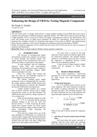
- 4. Dr.Yarub A. Estaitia , Int. Journal of Engineering Research and Applications www.ijera.com ISSN: 2248-9622, Vol. 6, Issue 8, (Part - 3) August 2016, pp.29-32 www.ijera.com 32|P a g e Figure(1) The circuit Diagram IV. CONCLUSIONS The overall aim of this project was to design and build a voltage regulator module (VRM) so it could be used to test magnetic components. This goal was realized and switching circuit is ready for testing of inductors. A complete switching circuit is now fully completed and working. This can now be used for testing of different types and sizes of inductors and analyzing their performance. The future for voltage regulator module (VRM) designers will be very demanding. As the currents increase and voltages decrease, stricter demands will be placed on the load line and thermal issues will become extremely important. In the future it is expected that the parasitic resistance between the regulator and microprocessor will become much more of an issue and it may be necessary to integrate the voltage regulator onto the microprocessor die but this will require a big breakthrough in silicon technologies. REFERENCES [1]. Investigation of candidate VRM topologies for future microprocessors, F.C.Y. Lee and others, IEEE Transactions on Power Electronics · December 2000, DOI: 10.1109/63.892832 · Source: IEEE Xplore. [2]. Synthesis and design of integrated- magnetic-circuit transformer for VRM application, R. -T. Chen ; Dept. of Electr. Eng., Nat. Taiwan Univ., Taipei, Taiwan ; Y. -Y. Chen, IEE Proceedings - Electric Po ...> Volume:153 Issue:3. [3]. Synthesis and design of integrated- magnetic-circuit transformer for VRM application R.-T. Chen and Y.-Y. Chen, The Institution of Engineering and Technology 2006 IEE Proceedings online no. 20050386 doi:10.1049/ip- epa:20050386. [4]. Rozman, A., Fellhoelter, K., Circuit considerations for fast sensitive, low- voltage loads in a distributed power system (1995), Proc. IEEE APEC'95. [5]. Xu, P., Ye, M., Wong, P.L., and Lee, F.C.: ‘Design of 48 V voltage regulator modules with a novel integrated magnetics’, IEEE Trans. Power Electron., 2002, 17, pp. 990–998. [6]. Chen, R.T., and Chen, Y.Y.: ‘A novel single stage push pull converter with integrated magnetics and ripple-free input current’. Trans. IEEE Power Electronics Specialist Conf., 2004, pp. 3848–3853.