2. 2
second inverter converts the 160VDC voltage into a quasi-
square-wave representation of a sin-wave having a
frequency of 55Hz with a peak voltage matching the high
voltage DC bus potential. A simple feed forward technique
regulates the AC secondary voltage to 115VAC while the
battery varies over a range of approximately 11V to 15V.
(Through component modification, 230VAC is possible.)
The aforementioned features are similar to those of at least
one commercially available battery inverter (Radio Shack,
Catalog number 22-132A). Thermal limiting on the
evaluation unit is approximately 120W at ambient
temperatures to 30oC (a little lower than the competitive unit)
in order to allow the unit to be operated without a heat-
sinking enclosure. This allows users to probe various points
in order to provide a better understanding of circuit
operation.
Primary Inverter Design
Input Filter
The primary-side inverter is comprised of a simple R-C input
filter. Capacitors, C5 and C6 provide a stiff, sag-free source
for the inverter bridge comprised of Q1 through Q4 as shown
in the schematic (see Appendix). To aid this process,
Resistor, R37 and ceramic, non-inductive capacitor, C7,
parallel C5 and C6. Automotive applications can be fraught
with voltage transients across the battery terminals. To
prevent these transients from exceeding the VCC voltage
ratings of the HIP4082 and other ICs on the primary inverter
section, R7, C4 and D3 clamp the VCC voltage to 16V or
less.
Primary Inverter Waveform Generation
To minimize the size of the secondary filter, a 50% duty cycle
square-wave was chosen for primary excitation. With a
nearly constant, low-ripple voltage, secondary filtering can
be minimized and ripple nearly eliminated. An inexpensive
Intersil ICM7555 timer was chosen. This timer, an improved
555 timer, reduces VCC to ground cross conduction current
spikes, thereby minimizing bias current requirements.
The timer, U1, operates in the astable mode, accomplished
by tying pins 2 and 6 of the timer together. The astable mode
requires only one resistor, R1, and one capacitor, C3. A 50%
duty-cycle square-wave is available at the “OUT” (pin 3)
terminal of timer, U1, as shown in Figure 1.
The timer ‘out’ pin drives the clock input, pin 3, of a CA4013
D-flip-flop connected as a divide by two circuit. To
accomplish the divide-by-two function, the QNOT output of
the flip-flop is fed back to its own data, D, input. The Q and
QNOT outputs of the CA4013 provide an exact 50% duty-
cycle square-wave at half the timer’s output frequency and
are applied to the ALI-BHI and the AHI-BLI gate control
inputs of the HIP4082 respectively as shown in Figure 2. The
ICM7555 clock frequency was chosen to be 120kHz so that
the primary inverter frequency would be 60kHz.
Choosing Proper Dead-Time
The dead-time chosen for eliminating shoot-through currents
in the Q1-Q4 and Q2-Q3 MOSFET pairs is determined by the
value of R2 connected between the DEL and VSS pins of the
HIP4082. The 15K value chosen provides approximately
0.5s of dead-time, sufficient to avoid shoot-through when
using RFP70N06 MOSFETs. Refer to the HIP4082 data
sheet, File Number 3676, Figure 16 for dead-time versus
delay resistance characteristics.
Controlling di/dt and Switching Losses
Choice of gate resistor values for R3-R5, and R8 is based
upon several factors. The gate resistors tailor the turn-on and
turn-off rise times of the power MOSFETs and the
commutating di/dt. The di/dt affects commutation losses and
body diode recovery losses. As di/dt increases, recovery
losses increase, but the commutation losses decrease. As
di/dt decreases, recovery losses decrease, and commutation
losses increase. Generally there is an ideal commutation di/dt
which minimizes the sum of these switching losses.
1
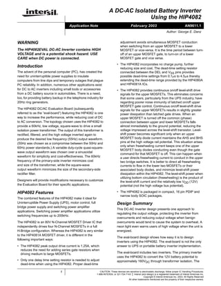
2
CH1 = 5V CH2 = 5V M = 2.5µs CH1 4.2V
C2 (MAX)
9V
C1 FREQ.
118.28kHz
FIGURE 1. 555 TIMER WAVEFORMS
1
2
CH1 = 10V CH2 = 10V M = 2.5µs CH1 4.2V
C2 (MAX)
13.8V
C1 FREQ.
59.544kHz
LOW
SIGNAL
AMPL.
FIGURE 2. INPUT WAVEFORMS TO THE HIP4082
Application Note 9611
3. 3
Inductances which are in series with each power MOSFET
also control di/dt. Stray inductance between the filter capacitor
and the positive and negative bus rails help reduce the
switching di/dt.
In the eval-board, no inductance is added to control the di/dt.
A small parasitic inductance exists naturally in the printed
circuit board and component layout. Secondary-side inverter
gate-to-source capacitors control the di/dt commutation rate.
Additionally, a snubber (R38-C27) was employed across the
inverter output terminals to control switching transients. The
gate-source capacitors help reduce the ringing at the
inverter bridge terminals associated with the output choke
employed to reduce EMI.
Bootstrap Supply Design
The bootstrap supply technique is a simple, cost-effective
way to power the upper MOSFET’s gate and provide bias
supply to the floating logic sections of the HIP4082. Only two
components per bridge phase are needed to implement the
bootstrap supply. For a full bridge driver such as the
HIP4082, diodes D1 and D2, and capacitors C1 and C2 are
all that is needed to provide this function as shown in the
schematic in the Appendix.
The bootstrap capacitor gets charged or “refreshed” using
the low voltage (VCC) bias supply. A fast recovery diode is
connected between the bootstrap capacitor and VCC, with
the anode going to VCC and the cathode to the capacitor.
The other side of the capacitor is tied to COM or VSS
potential through a low-side power MOSFET throughout the
period during which the low-side MOSFET or its body diode
is conductive. Since the body diode conduction depends on
some remaining load current at the time that an upper
MOSFET is turned off, it is generally wise to reserve a short
period during every PWM cycle to turn on the lower
MOSFET, thereby guaranteeing that refresh occurs.
The refresh time allotted must last long enough to replace all
of the charge that is sucked out of the bootstrap capacitor
during the time since the last refresh period ended. There
are 3 components of charge which must be replaced. The
least significant is that due to the bias supply needs of the
upper logic section of the HIP4082, which typically will be
145µA when the MOSFET is gated on and about 1.5mA
when it is gated off. Bootstrap diode leakage current will
normally be negligible, but should be investigated. The
required charge is the upper bias supply current of the
HIP4082 integrated over one PWM period.
The second component, usually very significant, is the charge
required to pump up the equivalent MOSFET input
capacitance to the VCC level. The charge, QGATE, is equal to
the product of the equivalent gate capacitance, CGATE, and
the magnitude of gate voltage applied, VCC. The power
dissipated in pumping this charge is the product of the charge,
QGATE, the applied voltage, VCC, and the frequency of
application, fPWM. Most MOSFET data sheets supply values
for QGATE at 10V and at 20V. Obtain the equivalent CGATE by
taking the charge given in the data sheet for 10V and dividing
it by 10. Multiply the equivalent CGATE by the actual operating
VCC to get the actual QGATE.
The third component of charge lost during each switching
cycle is that due to the recovery of the bootstrap diode. This
charge component is insignificant if one uses a fast or ultra-
fast recovery bootstrap diode. Ultra-fast recovery diodes are
recommended (see the Bill of Material included in the
Appendix).
The upper bias supply operating current will vary with PWM
duty-cycle. The upper bias current is typically 1.1mA when
driving a 1000pF load with a 50kHz switching voltage
waveform (at a 50% duty-cycle). This value represents the
sum of all three of the previously discussed components of
current. Figure 14 of the HIP4082 datasheet [1] shows typical
full bridge level-shift current as a function of switching
frequency (at a 50% duty-cycle). As duty-cycle decreases, the
level-shift current increases somewhat. The best way to
determine the exact level of current is to measure it at the
duty-cycle desired. In many applications, the duty-cycle is
constantly changing with time. Therefore a 50% duty-cycle
waveform is a good choice for purposes of determining
bootstrap average current requirements.
The level-shift current also tends to increase with frequency,
because the leading edge of each level-shift signal
incorporates a robust current pulse to guarantee that the
translation pulse is not interrupted by stray IC currents
induced by the high dv/dt levels which occur during
switching. Figure 14 of the HIP4082 data sheet includes this
effect also.
Special Concerns
When the HIP4082 IC first powers up, there is a 400ns to
500ns pulse applied to both lower MOSFET gates which
serves to charge the bootstrap capacitors for the first time.
This action corresponds with a simultaneous off pulse to
both upper MOSFETs through the level-shift circuitry. If it is
necessary to completely charge the bootstrap capacitors
upon power-up, then this pulse imposes limitations on the
size allowed for the bootstrap capacitors. If too large, they
may not get charged within the 400ns to 500ns window. The
start-up pulses are sent regardless of what state the input
logic signals (except for DIS) are in at the time.
In the event that MOSFETs are used with very large Gate-
Source input capacitances (or when several smaller
MOSFETs are paralleled) complete charging of the
bootstrap capacitors can be guaranteed by issuing lower
MOSFET turn-on pulses of a longer duration than the default
duration issued by the HIP4082. The peak current drawn
from the VCC supply can be quite severe in the case of a
1.0µF bootstrap capacitor, for example. In this example, it
would take 24A to charge the capacitor in 0.5µs. Obviously
the bootstrap diode equivalent series resistance, coupled
Application Note 9611
4. 4
with the additional trace impedances in the bootstrap
charging loop will not allow 24A to flow. Often the customer’s
power supply used for biasing the driver and control logic is
incapable of supplying this magnitude of current. For this
reason, much larger bypass capacitors are recommended
for the VCC supply than are used for the bootstrap
capacitors. A good rule of thumb is ten times greater. In the
example above, if the bootstrap circuit impedance is
estimated to be about 5Ω, then the peak current will be only
2.4A. The time required to charge up the bootstrap capacitor
(an exponential charge characteristic is assumed) to just
under 11V will be approximately 12µs. (24 times the charge
time allotted by default within the IC!) To avoid problems
when driving large MOSFETs or when paralleling MOSFETs
it is necessary to consider the low voltage bias supply’s
output impedance, the bias supply’s bypass capacitor
(located at the HIP4082 IC), the size of the bootstrap
capacitor (it should also be about 10 times the equivalent
input capacitance of the connected MOSFETs), and the
forward resistance characteristic of the chosen bootstrap
diode.
Transformer Specification
Current Product-to-Market needs often require having a
magnetics supplier design the magnetics devices in your
design. We followed this approach with respect to the eval-
board’s transformer and choke. The electronics designer
provides a detailed specification to the transformer supplier.
The specification should include the minimum frequency of
operation, the maximum applied voltage and waveform, the
continuous and overload current profiles, and operating
ambient temperature. Required transformer regulation must
also be specified. The transformer designer needs to know
this in order to size the transformer wire and leakage
inductance. The power handling capability and operating
frequency influences choice of core size and geometry and
ultimately the cost and size of the transformer. (Refer to the
Bill of Material included in the Appendix for information
regarding the transformer.)
It is important that the transformer designer have knowledge
of the transformer excitation waveform. The reason that this
is important is that the current waveshape dictates the form
factor or the value of RMS (root-mean-square) current that
will result for a given required average current. The size of
the filter capacitor, the equivalent series impedance of the
secondary, and the output voltage waveshape will determine
the current waveform and form factor. The RMS current
determines the power losses in the transformer and
temperature rise. To minimize ringing on the inverter bridge
of the primary inverter it will help to minimize the leakage
inductance of the transformer. For the DC-to-AC inverter
eval-board, power ferrite material, E core style PQ3230, was
used for the core.
In order to minimize transformer size and maximize winding
fill, the primary was formed of 3 separate windings which were
paralleled to supply the approximately 30ARMS required at
rated output power. Each primary winding’s DC resistance is
less than 10mΩ. There are two equal, but separate,
secondary power output windings. When series-connected,
these secondary power output windings provide 230VAC load
power. The US configured eval-boards are provided with
paralleled output windings for 115VAC operation. Series
connection via soldered jumper wires allows for 230VAC
operation, but this shouldn’t be attempted without changing
the power MOSFETs and the voltage ratings of several
capacitors. A 500V MOSFET with an rDS(ON) of 1.5Ω such as
the Intersil IRF830R would be a suitable device for 230VAC
operation. Besides having to double the capacitor voltage
ratings of C23, C27 and C13, the capacity of C23 and C27 will
have to be dropped by a factor of 4. This maintains the power
dissipation in resistors, R34 and R38 to remain as they are for
the 115VAC design.
A third secondary winding provides low voltage control
power to all of the secondary-side inverter logic and gate
drivers. This voltage is nominally 20.5V (peak of the square-
wave) when there is a nominal 13.6VDC applied to the
battery input terminals of the eval-board. This winding must
output at least 14V at the minimum battery voltage in order
to keep the series regulator out of saturation. This winding
carries less than 100mA, so winding gauge will be
determined more for strength than for current carrying
capacity.
Secondary Inverter Design
The secondary-side inverter and control is designed to
provide a near constant 115VAC to 120VAC, 55Hz output
voltage waveform. The inverter can supply approximately
120W to loads such as small fans, lights, radios and other
small electric appliances that might be handy to have with
you on a camping trip, for example.
In addition, a simple current trip circuit and an overtemp
limiter was incorporated in order to provide features similar
to a commercially available DC-to-AC inverter of similar
rating and purpose.
The secondary-side inverter includes the following functions:
• A high voltage input rectifier and filter
• A high voltage DC-to-AC inverter and control circuits,
providing over-current, thermal protection, and output
voltage regulation to compensate for widely varying
battery voltages and output current;
• A neon lamp to warn of the presence of high voltage and
ELECTRICAL SHOCK HAZARD. Details of these circuits
follow.
Input Filter and Rectifiers
There are two full wave rectifiers. One rectifies the 162V
secondary voltage to provide the DC high voltage bus for the
Application Note 9611
5. 5
inverter. Ultra-fast recovery, 3A rectifiers (UF5405), rectify
the 60kHz square-wave voltage waveform. Ultra-fast
recovery rectifiers reduce the recovery energy dissipated.
Even ultrafast diodes, such as the UF5405, forced a slight
reduction in the predicted output power rating of the inverter
due to higher than expected recovery energy loss. Addition
of some series impedance between the filter capacitor, C8,
and the rectifier bridge, possibly even relocation of the shunt
resistor, R23, would help to reduce this power. Users should
keep this in mind when designing their own solutions.
The choice of square-wave excitation waveform allows a
smaller rectifier filter capacitor to be used, while still
maintaining very low high voltage DC bus ripple.
The second rectifier provides control power to the linear
regulator, which in turn provides regulated 12VDC for all
secondary-side control and gate drivers. This voltage varies
from 15V to 23V as the battery voltage varies from 10V to
15V. A second, isolated winding from the transformer excites
this rectifier. Unlike the high voltage rectifier, this rectifier
bridge incorporates 1Ω of series resistance, R35, and a
relatively small filter capacitor, C9. No significant heating
occurred in the 1A UF4002 rectifiers. Filter ripple is controlled
by the linear regulator, U3, input (test point TP6). The low
current linear regulator provides 12V bias for all of the
secondary-side control, driver ICs, and for MOSFET gate
drive.
Secondary-Side Inverter
The secondary-side inverter functions include the power
MOSFETs Q6 through Q9, their associated gate resistors
and capacitors, the snubber, the current-sensing resistor, the
output choke, the indicator lamp and the filter.
The inverter topology is a full-wave H-bridge and synthesizes
a pseudo sin-wave by alternately switching on Q6 and Q9 for
positive half sin-waves and Q7 and Q8 for negative half sine-
waves. Since the inverter requires the ability to regulate the
RMS output voltage over a wide ranging DC battery input
voltage, some means of varying the conduction period of the
Q6-Q9 and Q7-Q8 pairs must be implemented.
The choice of square-wave output over sine-wave output
simplified the pulse-width-modulator (PWM) and minimized
MOSFET power dissipation. Figure 3 shows the actual
output voltage waveform.
Varying the width of the positive and negative conduction
periods inversely with the voltage level of the high voltage
bus maintains the RMS value of the output waveform
relatively constant.
Phase shifting two nearly perfect square-waves from the left
and right half-bridges making up the inverter produces the
waveforms shown in Figure 3. The left half-bridge includes
MOSFETs Q6 and Q8 and the right half-bridge includes
MOSFETs Q7 and Q9. The waveforms generated at the
common connections (sometimes referred to as the phase
node or phase terminal) of the MOSFET half-bridges appear
as shown in Figure 4.
Trace 1 is the voltage at the phase node of Q6 and Q8 and
Trace 2 is the voltage at the phase node of Q7 and Q9. The
vector difference between the two phase node voltages is
the output voltage shown in Figure 3.
The required phase-shift function is implemented by a simple
control circuit. The technique can be expanded to create
sinusoidal or other output waveform types with added
complexity, of course. The control circuits used in this design
will be discussed in the section, “Secondary Inverter Control
Circuits.”
The high voltage output waveform can exhibit a nasty
voltage transient, with the potential to mess up the output
voltage across the connected load and to possibly destroy
the high voltage gate driver, HIP2500, or the secondary-side
inverter MOSFETs. Therefore phase-to-phase and DC bus
snubbers were added. Resistor, R34 and capacitor, C23,
implement the bus snubber and resistor, R38 and capacitor,
C27, comprise the phase-to-phase snubber. Phase-to-phase
or “AC” snubbers allow their capacitors to completely charge
and discharge each cycle of the switching waveform and at
high switching frequencies will dissipate a lot of power. R38
and C27 were not used, but space for them was provided.
1
CH1 = 50V M = 2.5µs GLITCH CH1
FIGURE 3. SECONDARY-SIDE BRIDGE OUTPUT
Application Note 9611
6. 6
The energy required to charge a capacitor to a certain
voltage and discharge it to its original voltage level is the
product of the capacitance and the voltage attained across
the capacitor during the charging cycle. The AC snubber
dissipation is therefore: , where
fPWM = 55Hz. This fact is one reason that a high frequency
PWM modulation technique was avoided, namely that the
snubber power would have been quite substantial. The charge
transferal in the DC bus snubber is almost negligible, because
the capacitor voltage doesn’t appreciably change or switch
polarities like that of the AC snubber. Therefore the power
rating of the DC snubber’s series resistor can be minimal
(1/4W in this design).
Between the output banana jacks BJ3 and BJ4, and the
high voltage inverter a bifilar-wound choke was placed in
order to reduce conducted EMI at the load. Capacitor C13
aids in this regard.
Secondary Inverter Control Circuits
Simplicity and cost-effectiveness were the major design
goals. A feed-forward voltage regulation approach was
chosen to regulate the load RMS voltage within roughly 10%
over the expected load and battery input swings so as to
avoid the expense, complexity and stability problems
associated with a feedback approach. By using a
transformer with low secondary reflected resistance, most of
the regulation problem is limited to a “line regulation”
problem (battery changes from 10VDC to 15VDC) as
opposed to a “load regulation” problem.
To accomplish the regulation function using the filtered DC
bus voltage as a measured parameter, it was necessary to
determine the relationship between required duty cycle as a
function of the battery voltage which would result in an output
voltage of 115VAC(RMS) to the load. The function was
graphed and indicated that as the battery voltage increased,
the width of the positive and negative half-cycles should get
smaller, but the duty cycle reduction should be less than
proportionally reduced as the battery voltage increased. A
ramp which had positive curvature (i.e., positive first
derivative) would be able to synthesize this function where the
amount of positive curvature depended on the amount of
desired reduction in the duty-cycle. Figure 5 shows the
waveform necessary to produce the desired regulation
compensation.
The upper trace, Trace 2, is the triangle wave which is
compared with a reference signal proportional to the DC bus
voltage. When the triangle wave exceeds the reference
value, a clock pulse, Trace 1, is generated. The rising edge
of the clock pulse coincides with the moment that the triangle
wave becomes greater than the reference value proportional
to DC bus voltage.
When the DC bus voltage decreases, the reference wave
decreases, and the rising edge of the clock pulse advances
as shown in Figure 6.
The important point to remember is that as the DC bus
voltage decreases, the rising clock pulse occurs earlier and
earlier.
Also notice that the clock pulse frequency is double that of
the desired output frequency of the inverter, namely 110Hz
rather than 55Hz which is the desired excitation frequency to
the load. Figure 7 shows the clock waveform, TP10 (Trace 1),
and the associated Q (or QNOT) signal from flip-flop U5B
(Trace 2). The Q and QNOT waveforms are inverted from
each other at half the clock signal frequency and are
responsible for driving the phase-shifted half-bridge
comprised of MOSFETs Q7 and Q9.
A similar clock pulse (not shifted) coming from pin 3 of U8
produces an identical set of conditions on the Q and QNOT
outputs of flip-flop, U5A. Figure 8 shows the HIN (TP18) and
LIN (TP17) inputs of the phase-shifted half-bridge driver (right
side half-bridge). An identical set of signals will be seen at the
HIN and LIN inputs of the stationary (left side) half-bridge
driver, TP19 and TP20, respectively, responsible for driving the
stationary half-bridge comprised of MOSFETs Q6 and Q8.
1
2
CH1 = 100V CH2 = 100V M = 2.5µs CH2 64V
C2 (MAX)
172V
C1 FREQ.
56.024kHz
LOW
SIGNAL
AMPL.
FIGURE 4. SECONDARY-SIDE PHASE NODE WAVEFORMS
VBUS
2
CSNUBBER fPWM××
1
2
CH1 = 5V CH2 = 2V M = 2.5µs GLITCH CH2
C2 FREQ.
110.496Hz
FIGURE 5. SECONDARY-SIDE CONTROL WAVEFORMS
Application Note 9611
7. 7
The left and right half side half-bridges must be synchronized.
The left half-bridge switching is perfectly synchronized with
the minimum instances of the triangle wave and is therefore
fixed in phase with the triangle wave. The right half-bridge
slides with the level of the signal proportional to the DC bus
voltage level as previously mentioned. When the triangle wave
reaches a minimum, a positive rising pulse is output at pin 3 of
the ICM7555 timer, U8. This rising edge ‘clocks’ the U5A flip-
flop which will either result in a high level at U5A’s Q or QNOT
outputs, depending on the state of the data, D, input pin. It is
not important which goes high first, only that the toggling of
the Q and QNOT outputs of U5A alternate at each positive
clock pulse from pin 3 of U8. The timer’s output, pin 3, goes
low each time that the triangle wave reaches a peak.
Of paramount importance, however, is the need to
synchronize the state of U5B’s Q and QNOT outputs with
those of U5A. Arbitrarily the Q output of U5A was chosen to
drive the upper left MOSFET in the left half-bridge (QNOT
obviously drives the lower MOSFET). It is necessary that
whenever the upper MOSFET of the left half-bridge is gated
that the lower MOSFET in the right half-bridge also will be
gated sometime within the same half-cycle. To guarantee that
this happens it is necessary to connect either the Q or QNOT
output of U5A to the data, D, input of U5B. If the Q output of
U5A, which corresponds to the upper left MOSFET gate drive,
is chosen to drive the D input of U5B, the next clock pulse from
the phase-shifted clock which goes to U5B’s clock input pin
must gate the lower right MOSFET, which corresponds to the
LIN input of the right half-bridge driver, U9. Therefore the Q
output signal of U5B must drive the LIN input of U9 and the
QNOT signal of U5B must drive the HIN input of U9.
The waveforms in Figure 4 show the phase voltage
waveforms of the left and right half-bridges and the resulting
output voltage waveform shown in Figure 3. Notice that the
algebraic difference between Trace 2 and Trace 1 waveforms
precisely result in a waveform like that of Figure 3.
Unlike the HIP4082 and other members of the HIP408X
family, the HIP2500 high voltage half-bridge driver requires
external circuitry to insure that the upper and lower
MOSFETs in a half-bridge leg do not conduct
simultaneously. The quad AND-gate, U6, and resistors R24-
R27, and capacitors C14-C17 tailor the dead-time to the
needs of any application. Each Q and QNOT output from the
flip-flops go directly to one input of a two input AND-gate and
also through an R-C delay to the 2nd input of the AND-gate.
Only after the R-C delay can the output of an AND-gate go
high. Conversely, when any of the Q or QNOT outputs go
low, a zero is placed on one of the AND-gate inputs and the
AND-gate’s output immediately goes low. Therefore an ON-
DELAY is produced, but no corresponding OFF-DELAY is
produced.
Overcurrent Protection
An instantaneous overcurrent function senses the voltage
drop across R23 for the purposes of shutting down the
secondary-side inverter. The circuit comprising U7A, R28,
R29, R32, R36, shunt resistor R23 and capacitor, C32 dictate
the current trip level. The values shown in the schematic
should cause overcurrent trip at approximately 1.3A. The
voltage on the negative summing junction of U7A dictates the
1
2
CH1 = 5V CH2 = 2V M = 2.5µs GLITCH CH2
C2 FREQ.
110.04Hz
FIGURE 6. SECONDARY-SIDE CONTROL WAVEFORMS WITH
LOWER DC BUS VOLTAGE
1
2
CH1 = 5V CH2 = 5V M = 2.5µs GLITCH CH2
C2 FREQ.
55.552Hz
FIGURE 7. SECONDARY-SIDE FLIP-FLOP WAVEFORMS
1
2
CH1 = 5V CH2 = 5V M = 2.5µs GLITCH CH2
C2 FREQ.
55.872Hz
FIGURE 8. HIP2500 INPUT WAVEFORMS
Application Note 9611
8. 8
trip level based upon the divider action of R29 and R32. The
output of U7A goes to the SD input of both HIP2500 high
voltage half-bridge drivers, disabling them.
Once tripping has occurred, reset must be accomplished by
removing input voltage to the eval-board, as R28 provides
enough hysteresis such that even after the load current is
dropped to zero (no signal at the SHUNT resistor), the
voltage on the positive summing junction of U7A will exceed
that on the negative summing junction.
Overtemperature Protection
Resistors R10 - R12, R14, RT1 and diode D4, provide the
overtemperature function. Overtemperature does not shut
down the eval-board as in the case of overcurrent. Instead,
the duty-cycle of the output voltage waveform is reduced,
thereby reducing the RMS output voltage. This is
accomplished by faking the voltage control function into
thinking that the input voltage is higher than it really is.
When the thermistor, RT1, temperature increases, its
resistance decreases and the negative summing junction
voltage on pin 6 of U4B decreases. Eventually, when it falls
below the voltage on the positive summing junction, the
output, pin 7, of U4B rises. The voltage on the positive
summing junction is determined by the bias voltage and the
ratio of R11 to R12. The temperature at which this happens
is determined by the negative resistance characteristics of
the thermistor chosen and its temperature. RT1 is attached
by epoxy cement to one of the primary-side MOSFETs.
Diode D4, blocks the voltage on the output pin 7 of U4B from
affecting the inverter output voltage until after the
overtemperature condition has been reached.
Snubbers
A DC bus voltage snubber has been employed to control or
reduce transients across the bridge which might lead to
breakdown failure in either the MOSFETs or the HIP2500
drivers, or both. The bus voltage transients are snubbed by
the bus snubber comprised of resistor, R34 and capacitor,
C23. A good reference on snubber design is found in
Reference 2.
Conclusion
A simple, cost-effective solution to designing low to medium
voltage DC-to-AC inverters using the HIP4082 H-Bridge
Gate Driver has been shown using the HIP4082 DC/AC
Evaluation PC Board as a demonstration vehicle. Other
approaches using the same HIP4082 can certainly be
imagined and implemented with success.
Hopefully this application note will assist the designer in
getting started on his or her own design. This same HIP4082
IC can also be used in AC-to-DC converters, such as those
used in various motor controls and other high performance
DC voltage controllers.
WARNING
A neon lamp was placed across the output of the
inverter in order to warn users of the presence of HIGH
VOLTAGE AND POTENTIAL SHOCK HAZARD.
Application Note 9611
13. 13
All Intersil U.S. products are manufactured, assembled and tested utilizing ISO9000 quality systems.
Intersil Corporation’s quality certifications can be viewed at www.intersil.com/design/quality
Intersil products are sold by description only. Intersil Corporation reserves the right to make changes in circuit design, software and/or specifications at any time without
notice. Accordingly, the reader is cautioned to verify that data sheets are current before placing orders. Information furnished by Intersil is believed to be accurate and
reliable. However, no responsibility is assumed by Intersil or its subsidiaries for its use; nor for any infringements of patents or other rights of third parties which may result
from its use. No license is granted by implication or otherwise under any patent or patent rights of Intersil or its subsidiaries.
For information regarding Intersil Corporation and its products, see www.intersil.com
37 1 R32 100K 1% 1/4W
38 1 R14 200K 1% 1/4W
39 1 R17 20.0K 1% 1/4W
40 2 R15, R21 1.5Ω 1% 1/4W
41 1 R16, R30 12.1K 1% 1/4W
42 4 R18, R19, R20, R22 15Ω 1% 1/4W
43 1 R23 0.5Ω 1% 2W
44 4 R24, R25, R26, R27 4.7Ω 5% 1/4W
45 1 R28 38.3K 1% 1/4W
46 1 R31 681K 1% 1/4W
47 1 R33 82.5K 1% 1/4W
48 2 R35, R37 1Ω 5% 1/2W
49 21 TP1 - TP20, TP22 Test Point Berg, (BergStik)
50 1 T1 Transformer TNI, type T6905
51 2 U1, U8 ICM7555
52 1 U2 HIP4082IP
53 1 U3 MC78M12CT Motorola
54 2 U4, U7 CA3260AE Intersil
55 2 U5, U11 CD4013BE Intersil
56 1 U6 CD4081BE Intersil
57 2 U9, U10 HIP2500IP Intersil
58 4 HS1-4 576802B00000, Heat Sink AAVID
Parts List (Continued)
ITEM QUANTITY REFERENCE PART DESCRIPTION VENDOR/NO.
Application Note 9611