Computer Architecture I/O Organization
•
0 likes•187 views

Feza BUZLUCA, Bilgisayar Mimarisi Ders Notları, Bölüm 03, Giriş/Çıkış Organizasyonu, Asenkron yol (bellek) erişimi (IO Organization, Asynchronous bus (memory) access)

Recommended
More Related Content
What's hot
What's hot (17)
Similar to Computer Architecture I/O Organization
Similar to Computer Architecture I/O Organization (20)
More from Feza BUZLUCA
More from Feza BUZLUCA (20)
Recently uploaded
Recently uploaded (20)
Computer Architecture I/O Organization
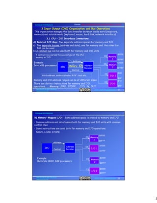
- 1. 1 3.1 Computer Architecture 2013 - 2020 Feza BUZLUCA www.faculty.itu.edu.tr/buzluca www.buzluca.info A) Isolated I/O Map: Two separate address spaces for memory and I/O a) Two separate busses (address and data), one for memory and the other for I/O can be used. b) A common bus can be used both for memory and I/O units. Memory and I/O address ranges can be of different sizes. There are distinct instructions for memory and I/O operations. Memory: LOAD, STORE, I/O: IN, OUT 3 Input Output (I/O) Organization and Bus Operations This organization manages the data transfer between inside world (registers, memory) and outside world (keyboard, mouse, hard disk, network interface). 3.1 CPU – I/O Interface Connections CPU Address Decoder Address I/O 1 CS $00 $0F Control Valid address, address strobe, R/W' clock etc. Memory 2 CS $1000 $FFFF I/O 2 CS $10 $FF CS $0000 $0FFF Memory 1 Memory- I/O A control line express the access type of the CPU; memory or I/O. Example: Intel x86 processors License: https://creativecommons.org/licenses/by-nc-nd/4.0/ 3.2 Computer Architecture 2013 - 2020 Feza BUZLUCA www.faculty.itu.edu.tr/buzluca www.buzluca.info B) Memory-Mapped I/O: Same address space is shared by memory and I/O • Common address and data busses both for memory and I/O units with common control lines • Same instructions are used both for memory and I/O operations. MOVE, LOAD, STORE CPU Address Decoder Address Control Memory 1 I/O 1 Memory 2 I/O 2 CS CS CS CS $0000 $0FFF $2000 $2FFF $1000 $1FFF $3000 $3FFF Example: Motorola 68XX, 68K processors
- 2. 2 3.3 Computer Architecture 2013 - 2020 Feza BUZLUCA www.faculty.itu.edu.tr/buzluca www.buzluca.info Separate Busses for Memory and I/O units: I/O Bus Interface Interface Peripheral Peripheral Common bus for Memory and I/O: Interface Interface Peripheral Peripheral CPU Common bus for memory and I/O CPU Memory Memory Bus Memory MemoryMemory 3.4 Computer Architecture 2013 - 2020 Feza BUZLUCA www.faculty.itu.edu.tr/buzluca www.buzluca.info 3.2 I/O Interface Module Peripherals are connected to CPUs over an I/O interface unit. Functions of an interface: • The data transfer rates of peripherals and the CPU are different. Checking the status of the peripheral, data buffering • Data conversion: Coding, encoding, different formats • Error detection • Signal conversion: Magnetic, electromechanic, electronic Example I/O Interface: Data Bus Buffer CPU Peripheral Control Status Handshaking Port A Data Port B Data Timing and Control CS RS0 RS1 R/W Control signals to all units IRQ
- 3. 3 3.5 Computer Architecture 2013 - 2020 Feza BUZLUCA www.faculty.itu.edu.tr/buzluca www.buzluca.info 3.3 Data Transfer Modes between I/O Interfaces and Memory 1.Programmed I/O (software polling): It is the responsibility of the processor a) periodically to check the status of the I/O interface (ready/busy, complete) b) to perform the data transfer between memory (registers) and I/O interface. Read status Data Ready?No Read data from I/O interface Write data to memory Yes If the I/O interface has finished the previous operation it sets the "COMPLETE" flag. The CPU reads data from the memory and writes it to the I/O interface. Read status Complete ?No Read data from memory Write data to I/O Interface Yes If the I/O interface has received data from a peripheral it sets the "READY" flag. The CPU reads data from the I/O interface and writes to the memory. Read from the I/O Interface: The CPU runs a program to check the status of the I/O interface. Write to the I/O Interface: If the CPU has data to send, it checks the status of the I/O interface. 3.6 Computer Architecture 2013 - 2020 Feza BUZLUCA www.faculty.itu.edu.tr/buzluca www.buzluca.info Disadvantage: The main disadvantage of this technique is the busy-waiting of the CPU while checking the status of the I/O units. Both operations about the I/O are performed by the CPU. a) Checking the status of the I/O units. During checking the status, the CPU cannot run other programs (busy-waiting). b) Data transfer is also performed by the CPU (The data flows over the CPU). Advantage: This technique is simple. Additional hardware units are not necessary. When the CPU does not have any tasks other than performing I/O operations or if the CPU cannot execute another program without performing the I/O operation, then busy-waiting is not a problem. For such systems programmed I/O is a simple and suitable technique for I/O operations. 1. Programmed I/O cont'd:
- 4. 4 3.7 Computer Architecture 2013 - 2020 Feza BUZLUCA www.faculty.itu.edu.tr/buzluca www.buzluca.info In the interrupt-driven technique the CPU sets the I/O interface to send an interrupt request if it is ready. Advantage: The CPU does not need to check the status continuously. The "busy- waiting" problem does not exist. The CPU can run other programs while the I/O interface is receiving data from or sending to a peripheral. The I/O interface will then interrupt the processor to request service when it is ready to exchange data with the CPU. The processor interrupts its current program, runs the interrupt service routine in which the data transfer is executed, and then resumes its former processing. In this technique the CPU does not check the status, but it is still the responsibility of the processor to perform the data transfer. Disadvantage: Interrupt processing has its own overhead (saving return address, program status, registers and performing some other operations) (Section 4). At the end of the service routine, return-address and program status are read. Interrupt-driven I/O is not suitable for applications where I/O operations are performed very frequently. 2. Interrupt-Driven I/O: License: https://creativecommons.org/licenses/by-nc-nd/4.0/ 3.8 Computer Architecture 2013 - 2020 Feza BUZLUCA www.faculty.itu.edu.tr/buzluca www.buzluca.info 3.Direct Memory Access (DMA): In the programmed and interrupt-driven techniques the CPU is responsible for transferring data between memory and I/O interfaces. The CPU must execute a number of instructions for each I/O transfer. The direct memory access (DMA) technique involves an additional hardware module on the system bus called the DMA controller (DMAC). The DMAC is capable of acting as the CPU and of taking over control of the system bus from the processor. When the CPU needs to read or write a block of data, it initializes the DMAC by sending the necessary information (address, size, transfer mode etc.). So, it has delegated the I/O operation to the DMAC. The CPU can continue with its other programs during the transfer of data. The data do not flow over the CPU. The DMAC uses the system bus only when the processor does not need it, or it must force the processor to suspend the bus operations temporarily. The DMA technique is suitable for applications where large volumes of data are transferred and I/O operations are performed very frequently. An additional hardware module (DMAC) is necessary. DMA is explained in Section 5.
- 5. 5 3.9 Computer Architecture 2013 - 2020 Feza BUZLUCA www.faculty.itu.edu.tr/buzluca www.buzluca.info Summary of Data Transfer Modes: Task Method Check the status of the I/O Interface Data transfer between I/O Interface and memory Programmed I/O: CPU (Program) DMA: The table below shows which device is responsible for checking the status of the I/O Interface and transferring the data. CPU (Program) Interrupt driven I/O: Interrupt Mechanism CPU (ISR) DMAC DMAC 3.10 Computer Architecture 2013 - 2020 Feza BUZLUCA www.faculty.itu.edu.tr/buzluca www.buzluca.info Problems: a) Has the sender sent the data (Is the data on the data bus valid)? b) Has the receiver received the data (Is the receiver busy)? Strobe 3.4 Asynchronous Data Transfer: 1. Strobe Control: Source Destination Data Data Valid Data Strobe (Source) 1 2 3 4a) Source-initiated strobe : StrobeSource Destination Data Data Valid Data Strobe (Destination) 1 2 3 4 b) Destination-initiated strobe: The duration of valid data is predetermined according the speed of the destination. The source does not know whether the destination has really received the data. Time to transfer (sample) the data from the bus is predetermined according the speed of the source. The destination does not know whether the source has really sent the data.
- 6. 6 3.11 Computer Architecture 2013 - 2020 Feza BUZLUCA www.faculty.itu.edu.tr/buzluca www.buzluca.info Data valid 2. Handshaking: Source Destination Data Data Valid Data Data valid (Source) 1 2 3 4 a) Source-initiated: Data accepted 5 6Data accepted (Destination) Data validSource Destination Data Data Valid Data Ready (Destination) 1 2 3 4b) Destination-initiated: Ready/busy 5 6 Data valid (Source) The source waits for the “Data accepted" signal. To avoid "infinite waiting" when the “Data accepted" signal does not respond due to an error, a time-out mechanism must be used. The destination waits until the “Data valid" signal is received. To avoid infinite waiting a time-out mechanism is necessary. 3.12 Computer Architecture 2013 - 2020 Feza BUZLUCA www.faculty.itu.edu.tr/buzluca www.buzluca.info 3.5 Data Transfer between the CPU – Memory (or I/O Interface) CPUs also use synchronous or asynchronous data transfer mechanisms to access the memory. 3.5.1 Synchronous bus operation with strobe For example, MC 6802 uses strobe mechanism in memory access. This operation is also synchronized with the clock signal (E) of the processor. The Valid Memory Address (VMA) signal indicates that the address on the bus is valid and initiates the bus cycle (strobe). When the clock signal goes from 1 to 0 data is latched and the bus cycle is terminated. Read cycle of MC6802:
- 7. 7 3.13 Computer Architecture 2013 - 2020 Feza BUZLUCA www.faculty.itu.edu.tr/buzluca www.buzluca.info Chip select is send to the memory via the address decoder. When the clock signal goes from 1 to 0 the bus cycle is terminated. Write cycle of MC6802: Similarly, "write cycle" also starts with the activation of the VMA. License: https://creativecommons.org/licenses/by-nc-nd/4.0/ 3.14 Computer Architecture 2013 - 2020 Feza BUZLUCA www.faculty.itu.edu.tr/buzluca www.buzluca.info 3.5.2 Asynchronous bus operations with handshaking For example, MC68000 access the memory (and I/O interfaces) using the asynchronous handshaking mechanism. It can also use the strobe mechanism that is synchronized with the clock signal (E) like the processors of the 68xx family. MC68000 Data Bus D15-D0 AS UDS LDS VMA VPA E Asynchronous Bus Control 6800 Peripheral/memory control Address Bus A23-A1 R/W DTACK Address line A0 is used inside the processor to control two other signals: UDS' and LDS'. Data bus is 16 bits. But its upper and lower 8-bit parts can also be used separately.
- 8. 8 3.15 Computer Architecture 2013 - 2020 Feza BUZLUCA www.faculty.itu.edu.tr/buzluca www.buzluca.info • AS' (Address Strobe): It is asserted (active low) by the processor to indicate that a valid memory address exists on the address bus. It starts the bus cycle. First handshaking signal. • UDS' (Upper Data Strobe) and LDS’ (Lower Data Strobe): They determine the size of the data being accessed (word or byte). Word: Both are asserted (low). Byte (odd address): LDS' asserted, D0-D7 used Byte (even address): UDS' asserted, D8-D15 used • DTACK' (Data Transfer Acknowledge): Handshaking input pin of 68000 Handshake signal generated by the device (memory/interface) being accessed indicates that the data bus contents are valid and that the 68000 may proceed with the data transfer. • VPA' (Valid Peripheral Address): This input informs the 68k that it has addressed a 6800 peripheral and that the data transfer should be synchronized with the E clock. If it is asserted during a bus operation (AS' is active) 68000 acts like 68xx and uses VMA and E signals to access the peripheral. Control Signals of MC68000 used for memory access 3.16 Computer Architecture 2013 - 2020 Feza BUZLUCA www.faculty.itu.edu.tr/buzluca www.buzluca.info MC68000 - Memory (I/O Interface) Connection MC68000 accesses memory (and I/O interfaces) using asynchronous handshaking mechanism. It can also act as a processor of the 68xx family and perform a synchronous bus operation started with a strobe (VMA). 68000 Memory or I/O Interface CSAddress1 Address2 VPA If the device (memory) cannot generate the DTACK signal. Delay depends on the access time of the memory. A device that is accessed using asynchronous handshaking mechanism Memory or I/O Interface Decoder E VMA CS Synchronous device DTACK is not used UDS,LDS Address Decoder Address AS DTACK DTACK Delay : From other asynchronous devices
- 9. 9 3.17 Computer Architecture 2013 - 2020 Feza BUZLUCA www.faculty.itu.edu.tr/buzluca www.buzluca.info DTACK (from device) (Must be negated) Ready ReadyW W Address is valid Address is validAS Bus Cycle Memory I/O Read Bus Cycle (Slow) Memory / I/O Read Valid Address Valid AddressA(23 -1) ReadR/W Read MC68000 Asynchronous Read-Cycle Timing States S0 S2 S4S1 S3 S5 S6 S7 S0 S1 S2 S3 S4 W W W W S5 S6 S7 CLK Data from Memo DataD(15 - 0) If the DTACK is not asserted the processor inserts wait states. On the falling edge at the end of S6 (start of S7) data is latched from the bus. LDS UDS 3.18 Computer Architecture 2013 - 2020 Feza BUZLUCA www.faculty.itu.edu.tr/buzluca www.buzluca.info CLK WriteR/W Write Ready ReadyW DTACK MC68000 Asynchronous Write-Cycle Timing Bus Cycle Memory/I/O Write Bus Cycle (Slow) Memory / I/O Write S0 S2 S4S1 S3 S5 S6 S7 S0 S1 S2 S3 S4 W WS5 S6 S7 Valid Address Valid AddressA(23 -1) Data DataD(15 - 0) Address is valid Address is validAS LDS UDS At the end of S6, DTACK’ is checked. If it is not asserted (memory could not latch data) wait states are inserted.
- 10. 10 3.19 Computer Architecture 2013 - 2020 Feza BUZLUCA www.faculty.itu.edu.tr/buzluca www.buzluca.info Avoiding Infinite Waiting MC68000 has an exception input called BERR’ (Bus Error) that can be asserted by an external logic if an error in the current bus cycle is detected. If this input is asserted (active 0) the 68000 terminates the current bus cycle, saves the current status into the stack (accessed address, current instruction etc.), and jumps to an exception handler program. BERR' will be explained in the chapter “Exceptions”. To avoid infinite waiting a counter can be connected to the BERR' as shown below: If the bus takes (AS' is active) longer than expected, BERR' is asserted. AS CLR 68000 BERR In this example: Counts until 10 (1010) (10µs) If no bus (AS'=1) operation, the counter is cleared. E (enable) Vcc Continuously enabled 4-bit CounterQ3 Q2 Q1 Q0 1 MhzCLK 3.20 Computer Architecture 2013 - 2020 Feza BUZLUCA www.faculty.itu.edu.tr/buzluca www.buzluca.info 8/16-bit Bus operations in MC68000 (access to odd/even addresses) In MC68000, the width of the data bus is 16 bits. Instructions can operate on 8, 16 or 32-bit operands (bus operations). Therefore, 8-bit memories are connected to 16-bit data bus in parallel. 68000 Memory1 (Even) Memory2 (Odd) D15-D8 D7-D0 0 2 4 : 1 3 5 : 8-bit memories To specify which memory is being accessed the MC68000 has two outputs: UDS' (Upper Data Strobe) and LDS' (Lower Data Strobe). The value of internal address line A0 determines the values of UDS' and LDS'. UDS LDS D15-D8 D7-D0 Description: H H --- --- No bus operation H L --- Data Byte access to an odd address A0=1 L H Data --- Byte access to an even address A0=0 L L Data Data Word access to an even address A0=0 UDS LDS
- 11. 11 3.21 Computer Architecture 2013 - 2020 Feza BUZLUCA www.faculty.itu.edu.tr/buzluca www.buzluca.info Address: (A0 is in the processor) A23A22 ..... A1 A0 UDS LDS MOVE.B ($000000),D1 0 0 ..... 0 0 0 1 MOVE.B ($000001),D1 0 0 ..... 0 1 1 0 MOVE.W ($000000),D1 0 0 ..... 0 0 0 0 MOVE.W ($000001),D1 Exception: Address error Example: D15-D8 D7-D0 Address Decoder A23-A1 (as necessary) AS EN Memory1 (Even) 0 2 4 : A23-A1 Memory2 (odd) 1 3 5 : LDS CS Example: $000000 Address1 Ex: $100000 Address2 DTACK to 68000 Delay 1 8-bit memories UDS CS 3.22 Computer Architecture 2013 - 2020 Feza BUZLUCA www.faculty.itu.edu.tr/buzluca www.buzluca.info 3.22 E In the example on the right following units are connected to the MC68000 : One serial communication interface (MC6850), a total of 4Kx8 ROM (2x 2716) and total of 4Kx8 SRAM (2x 4016) . Only two address lines A13 and A12 are used for address decoding. The serial communication interface (MC6850) is connected as a synchronous unit (VMA and E are used). Note: It communicates with its peer interface using the asynchronous mechanism. Between the CPU and memories data transfer occurs according to the asynchronous handshaking mechanism (AS and DTACK are used). Since ROMs are not written to, UDS/LDS lines are not used to select these units. Example:
- 12. 12 3.23 Computer Architecture 2013 - 2020 Feza BUZLUCA www.faculty.itu.edu.tr/buzluca www.buzluca.info Function Code Outputs in MC68000 MC68000 has 3 outputs that indicate the type of the operations: Function Codes Outputs: FC2, FC1, FC0. These outputs get valid values in each bus cycle (when AS' is asserted) and indicate the type of the operation. FC2 FC1 FC0 Description: 0 0 0 Undefined (Reserved) 0 0 1 User Mode, Data access (User Data) 0 1 0 User Mode, Program access (User Program) 0 1 1 Undefined (Reserved) 1 0 0 Undefined (Reserved) 1 0 1 Supervisor Mode, Data access (Supervisor Data) 1 1 0 Supervisor Mode, Program access (Supervisor Program) 1 1 1 Interrupt Acknowledge These outputs can be used in address decoding. • Access to specific devices and memory addresses can be restricted. These addresses can be accessed only in supervisor mode. • Separate memory spaces can be created for programs and data. User and supervisor modes are explained in section 4.5.1 Privilege Modes. 3.24 Computer Architecture 2013 - 2020 Feza BUZLUCA www.faculty.itu.edu.tr/buzluca www.buzluca.info DataProgram Placing separate program and data memories to the same address space In this example, by using the FC0 output of the MC68000 two separate memory modules are placed into the same address space. One module is selected when FC0 = 0 (program access). The second one is selected if FC0 = 1 (data access). D15-D8 D7-D0 Address Decoder A23-A1 (as necessary) AS EN Address 1 LDS UDS Mem. 2a Data (Even) A23-A1 Mem. 2b Data (odd) CSCS A23-A1 FC0 Memory 1a Program (Even) CS A23-A1 CS Mem. 1b Program (odd) Address 2 Address 3 Example: