
Recommended
More Related Content
What's hot
What's hot (20)
Viewers also liked
Viewers also liked (20)
Similar to 8086 Microprocessor Pin Configuration and Signal Description
Similar to 8086 Microprocessor Pin Configuration and Signal Description (20)
More from aviban
Recently uploaded
Recently uploaded (20)
8086 Microprocessor Pin Configuration and Signal Description
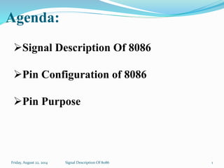
- 1. Agenda: Friday, August 22, 2014 Signal Description Of 8086 Signal Description Of 8086 Pin Configuration of 8086 Pin Purpose 1
- 2. Friday, August 22, 2014 Signal Description Of 8086 2 Signal Description of 8086 1. Available with 3 clock rates(viz. 5, 8 & 10 MHz) 2. 40 pin CERDIP or plastic package. 3. Operates in single as well as in multiprocessor configuration to achieve high performance. 4. Some pins serves particular function in minimum mode & other function in maximum mode. 5. Signal Category Groups Signals with common function in both mode Signals with Special function in minimum mode Signals with Special function in maximum mode
- 3. Friday, August 22, 2014 Signal Description Of 8086 3 1 2 3 4 5 6 7 8 9 10 11 12 13 14 15 16 17 18 19 20 40 39 38 37 36 35 34 33 32 31 30 29 28 27 26 25 24 23 22 21 GND AD0-AD14 NMI INTR GND VCC(+5V) RESET CLK AD15 RD MN/MX RQ/GT0 LOCK S1 S2 S0 QS0 TEST READY A16/S3 A17/S4 A18/S5 A19/S6 BHE/S7 RQ/GT1 QS1 8086 Interrupt Control Maximum Mode Time Multiplexed memory I/O address & data lines Time Multiple xed address & status lines Minimum Mode HOLD HLDA WR M/IO DT/R DEN ALE INTA
- 4. Friday, August 22, 2014 Signal Description Of 8086 4 Abbreviations Maximum Mode AD0-AD15 ≡ Address GND ≡Ground INTR ≡ Interrupt Return CLK ≡ Clock Input VCC ≡ Power Supply BHE ≡ Bus High Enable RD ≡ Read INTR ≡ Interrupt Request NMI ≡ Non Maskable Interrupt MN/MX ≡ Min/Max A16/S3, A17/S4, A18/S5, A19/S6 ≡ Multiplexed Address & Status Lines Minimum Mode M/I/O ≡ Memory I/O INTA ≡ Interrupt Acknowledge ALE ≡ Address Latch Enable DT/R ≡ Data Transmit/Receive DEN ≡ Data Enable HLDA ≡ Hold Acknowledge
- 5. Friday, August 22, 2014 Signal Description Of 8086 5 Pin Purpose of 8086 1. Bus High Enable BHE – indicates transfer of data over high order(D8-D15) 2. Clock Input CLK- Basic timing for processor operations & bus control activity. 3. Reset – causes processor to stop current activity & start execution from FFFFFH. 4. Vcc- Power supply for internal circuit operations. 5. GND- Ground for internal circuit.
- 6. Friday, August 22, 2014 Signal Description Of 8086 6 7. MN/MX- finds processors operating mode. i.e. minimum or maximum mode. 8.Intrrupt Acknowledge INTA– Admit interrupt 9. Address Latch Enable ALE-Availability of valid address on address/data lines, and is connected to latch enable input of latches. 10. Test- This Input is examined by a ‘WAIT’ instructions, If TEST input goes low then execution will continue else processor remain in an ideal state. Cont’d…
- 7. Friday, August 22, 2014 Signal Description Of 8086 7 11. Hold Acknowledge HLDA- When HOLD line goes high, it indicates to the processor that another master is requesting the bus access. 12.Data Enable– Indicates availability of valid data over address/ data lines. 13. Data Transmit/Receive DT/R-Used to decide the direction of data flow through transreceiver. deal state. Cont’d…