SlideShare a Scribd company logo
1 of 14
The 8086 CPU is divided into two independent functional units:
 Bus Interface Unit (BIU)
 Execution Unit (EU)
Features of 8086 Microprocessor:
 Intel 8086 was launched in 1978.
 It was the first 16-bit microprocessor.
 This microprocessor had major improvement over the execution speed of 8085.
 It is available as 40-pin Dual-Inline-Package (DIP).
 It is available in three versions:
o 8086 (5 MHz)
o 8086-2 (8 MHz)
o 8086-1 (10 MHz)
 It consists of 29,000 transistors.
Bus Interface Unit (BIU)
The function of BIU is to:
 Fetch the instruction or data from memory.
 Write the data to memory.
 Write the data to the port.
 Read data from the port.

Instruction Queue
1. To increase the execution speed, BIU fetches as many as six instruction bytes ahead to
time from memory.
2. All six bytes are then held in first in first out 6 byte register called instruction queue.
3. Then all bytes have to be given to EU one by one.
4. This pre fetching operation of BIU may be in parallel with execution operation of EU,
which improves the speed execution of the instruction.
5.
Execution Unit (EU)
The functions of execution unit are:
 To tell BIU where to fetch the instructions or data from.
 To decode the instructions.
 To execute the instructions.
The EU contains the control circuitry to perform various internal operations. A decoder in EU
decodes the instruction fetched memory to generate different internal or external control signals
required to perform the operation. EU has 16-bit ALU, which can perform arithmetic and logical
operations on 8-bit as well as 16-bit.
General Purpose Registers of 8086
These registers can be used as 8-bit registers individually or can be used as 16-bit in pair to have
AX, BX, CX, and DX.
1. AX Register: AX register is also known as accumulator register that stores operands for
arithmetic operation like divided, rotate.
2. BX Register: This register is mainly used as a base register. It holds the starting base
location of a memory region within a data segment.
3. CX Register: It is defined as a counter. It is primarily used in loop instruction to store
loop counter.
4. DX Register: DX register is used to contain I/O port address for I/O instruction.
Segment Registers
Additional registers called segment registers generate memory address when combined with
other in the microprocessor. In 8086 microprocessor, memory is divided into 4 segments.
1. Code Segment (CS): The CS register is used for addressing a memory location in the
Code Segment of the memory, where the executable program is stored.
2. Data Segment (DS): The DS contains most data used by program. Data are accessed in
the Data Segment by an offset address or the content of other register that holds the offset
address.
3. Stack Segment (SS): SS defined the area of memory used for the stack.
4. Extra Segment (ES): ES is additional data segment that is used by some of the string to
hold the destination data.
Flag Registers of 8086
Fig. 3: Flag Register of 8086
Flags Register determines the current state of the processor. They are modified automatically by
CPU after mathematical operations, this allows to determine the type of the result, and to
determine conditions to transfer control to other parts of the program. 8086 has 9 flags and they
are divided into two categories:
1. Conditional Flags
2. Control Flags
Conditional Flags
Conditional flags represent result of last arithmetic or logical instruction executed. Conditional
flags are as follows:
 Carry Flag (CF): This flag indicates an overflow condition for unsigned integer
arithmetic. It is also used in multiple-precision arithmetic.
 Auxiliary Flag (AF): If an operation performed in ALU generates a carry/barrow
from lower nibble (i.e. D0 – D3) to upper nibble (i.e. D4 – D7), the AF flag is set i.e.
carry given by D3 bit to D4 is AF flag. This is not a general-purpose flag, it is used
internally by the processor to perform Binary to BCD conversion.
 Parity Flag (PF): This flag is used to indicate the parity of result. If lower order 8-bits of
the result contains even number of 1’s, the Parity Flag is set and for odd number of 1’s,
the Parity Flag is reset.
 Zero Flag (ZF): It is set; if the result of arithmetic or logical operation is zero else it is
reset.
 Sign Flag (SF): In sign magnitude format the sign of number is indicated by MSB bit. If
the result of operation is negative, sign flag is set.
 Overflow Flag (OF): It occurs when signed numbers are added or subtracted. An OF
indicates that the result has exceeded the capacity of machine.
Control Flags
Control flags are set or reset deliberately to control the operations of the execution unit. Control
flags are as follows:
1. Trap Flag (TP):
a. It is used for single step control.
b. It allows user to execute one instruction of a program at a time for debugging.
c. When trap flag is set, program can be run in single step mode.
2. Interrupt Flag (IF):
a. It is an interrupt enable/disable flag.
b. If it is set, the maskable interrupt of 8086 is enabled and if it is reset, the interrupt
is disabled.
c. It can be set by executing instruction sit and can be cleared by executing CLI
instruction.
3. Direction Flag (DF):
a. It is used in string operation.
b. If it is set, string bytes are accessed from higher memory address to lower
memory address.
c. When it is reset, the string bytes are accessed from lower memory address to
higher memory address.
8086/88 Device Specifications
 Both are packaged in DIP (Dual In-Line Packages).
 8086: 16-bit microprocessor with a 16-bit data bus
 8088: 16-bit microprocessor with an 8-bit data bus.
 Both are 5V parts:
 8086: Draws a maximum supply current of 360mA.
 8086: Draws a maximum supply current of 340mA.
 80C86/80C88: CMOS version draws 10mA with temp spec -40 to 225degF.
 Input/Output current levels:
o Yields a 350mV noise immunity for logic 0 (Output max can be as high as 450mV
while input max can be no higher than 800mV).
o This limits the loading on the outputs.
8086/88 Pinout
8086/88 Pinout
 Pin functions:
 AD15-AD0
o Multiplexed address(ALE=1)/data bus(ALE=0).
 A19/S6-A16/S3 (multiplexed)
o High order 4 bits of the 20-bit address OR status bits S6-S3.
 M/IO
o Indicates if address is a Memory or IO address.
 RD
o When 0, data bus is driven by memory or an I/O device.
 WR
o Microprocessor is driving data bus to memory or an I/O device. When 0, data bus
contains valid data.
 ALE (Address latch enable)
o When 1, address data bus contains a memory or I/O address.
 DT/R (Data Transmit/Receive)
o Data bus is transmitting/receiving data.
 DEN (Data bus Enable)
o Activates external data bus buffers.
8086/88 Pinout
 Pin functions:
 S7, S6, S5, S4, S3, S2, S1, S0
o S7: Logic 1, S6: Logic 0.
o S5: Indicates condition of IF flag bits.
o S4-S3: Indicate which segment is accessed during current bus cycle:
o S2, S1, S0 : Indicate function of current bus cycle (decoded by 8288).
8086/88 Pinout
 Pin functions:
 INTR
o When 1 and IF=1, microprocessor prepares to service interrupt. INTA becomes
active after current instruction completes.
 INTA
o Interrupt Acknowledge generated by the microprocessor in response to INTR.
Causes the interrupt vector to be put onto the data bus.
 NMI
o Non-maskable interrupt. Similar to INTR except IF flag bit is not consulted and
interrupt is vector 2.
 CLK
o Clock input must have a duty cycle of 33% (high for 1/3 and low for 2/3s)
 VCC/GND
o Power supply (5V) and GND (0V).
8086/88 Pinout
 Pin functions:
 MN/ MX
o Select minimum (5V) or maximum mode (0V) of operation.
 BHE
o Bus High Enable. Enables the most significant data bus bits (D 15 -D 8 ) during a
read or write operation.
 READY
o Used to insert wait states (controlled by memory and IO for reads/writes) into the
microprocessor.
 RESET
o Microprocessor resets if this pin is held high for 4 clock periods.
o Instruction execution begins at FFFF0H and IF flag is cleared.
 TEST
o An input that is tested by the WAIT instruction.
o Commonly connected to the 8087 coprocessor.
8086/88 Pinout
 Pin functions:
 HOLD
o Requests a direct memory access (DMA). When 1, microprocessor stops and
places address, data and control bus in high-impedance state.
 HLDA (Hold Acknowledge)
o Indicates that the microprocessor has entered the hold state.
 RO/GT1 and RO/GT0
o Request/grant pins request/grant direct memory accesses (DMA) during
maximum mode operation.
 LOCK
o Lock output is used to lock peripherals off the system. Activated by using the
LOCK: prefix on any instruction.
 QS1 and QS0
o The queue status bits show status of internal instruction queue. Provided for
access by the numeric coprocessor (8087).
8284A Clock Generator
 Basic functions:
 Clock generation.
 RESET synchronization.
 READY synchronization.
 Peripheral clock signal.
 Connection of the 8284 and the 8086.
8284A Clock Generator
 Clock generation:
o Crystal is connected to X1 and X2.
o XTAL OSC generates square wave signal at crystal's frequency which feeds:
 An inverting buffer (output OSC) which is used to drive the EFI input of other 8284As.
 2-to-1 MUX
 F/ C selects XTAL or EFI external input.
o The MUX drives a divide-by-3 counter (15MHz to 5MHz).
o This drives:
 The READY flipflop (READY synchronization).
 A second divide-by-2 counter (2.5MHz clk for peripheral components).
 The RESET flipflop.
 CLK which drives the 8086 CLK input.
8284A Clock Generator
 RESET:
o Negative edge-triggered flipflop applies the RESET signal to the 8086 on the
falling edge.
o The 8086 samples the RESET pin on the rising edge.
o Correct reset timing requires that the RESET input to the microprocessor
becomes a logic 1 NO LATER than 4 clocks after power up and stay high for at
least 50us.
BUS Buffering and Latching
 Demultiplexing the Buses:
o Computer systems have three buses:
 Address
 Data
 Control
o The Address and Data bus are multiplexed (shared) due to pin limitations on the
8086.
 The ALE pin controls a set of latches.
o All signals MUST be buffered.
 Latches buffer for A 0 -A 15 .
 Control and A 16 -A 19 + BHE are buffered separately.
 Data bus buffers must be bi-directional buffers (BB).
o BHE : Selects the high-order memory bank.
BUS Buffering and Latching
BUS Timing
 Writing:
 Dump address on address bus.
 Dump data on data bus.
 Issue a write ( WR ) and set M/ IO to 1.
BUS Timing
 Reading:
 Dump address on address bus.
 Issue a read ( RD ) and set M/ IO to 1.
 Wait for memory access cycle.
BUS Timing
 Bus Timing:
BUS Timing
 During T 1 :
 The address is placed on the Address/Data bus.
 Control signals M/ IO , ALE and DT/ R specify memory or I/O, latch the address onto the
address bus and set the direction of data transfer on data bus.
 During T 2 :
 8086 issues the RD or WR signal, DEN , and, for a write, the data.
 DEN enables the memory or I/O device to receive the data for writes and
the 8086 to receive the data for reads.
 During T 3 :
 This cycle is provided to allow memory to access data.
 READY is sampled at the end of T 2 .
 If low, T 3 becomes a wait state.
 Otherwise, the data bus is sampled at the end of T 3 .
 During T 4 :
 All bus signals are deactivated, in preparation for next bus cycle.
 Data is sampled for reads, writes occur for writes.
BUS Timing
 Timing:
o Each BUS CYCLE on the 8086 equals four system clocking periods (T states).
o The clock rate is 5MHz , therefore one Bus Cycle is 800ns .
o The transfer rate is 1.25MHz .
o Memory specs (memory access time) must match constraints of system timing.
o For example, bus timing for a read operation shows almost 600ns are needed to
read data.
 However, memory must access faster due to setup times, e.g. Address
setup and data setup.
 This subtracts off about 150ns .
 Therefore, memory must access in at least 450ns minus another 30-40ns
guard band for buffers and decoders.
 420ns DRAM required for the 8086.
BUS Timing
 READY:
o An input to the 8086 that causes wait states for slower memory and I/O
components.
o A wait state (T W ) is an extra clock period inserted between T 2 and T 3 to
lengthen the bus cycle.
 For example, this extends a 460ns bus cycle (at 5MHz clock) to 660ns .
o Text discusses role of 8284A and timing requirements for the 8086.
MIN and MAX Mode
 Controlled through the MN/ MX pin.
 Minimum mode is cheaper since all control signals for memory and I/O are generated
by the microprocessor.
 Maximum mode is designed to be used when a coprocessor (8087) exists in the system.
 Some of the control signals must be generated externally, due to redefinition of certain
control pins on the 8086.
o The following pins are lost when the 8086 operates in Maximum mode .
 ALE
 WR
 IO/ M
 DT/ R
 DEN
 INTA
 This requires an external bus controller: The 8288 Bus Controller .
8288 Bus Controller
 Separate signals are used for I/O ( IORC and IOWC ) and memory ( MRDC and MWTC
).
 Also provided are advanced memory ( AIOWC ) and I/O ( AIOWC ) write strobes plus
INTA .
MAX Mode 8086 System

More Related Content

What's hot

Presentation on 8086 microprocessor
Presentation on 8086 microprocessorPresentation on 8086 microprocessor
Presentation on 8086 microprocessorDiponkor Bala
 
8086 module 1 & 2 work
8086 module 1 & 2   work8086 module 1 & 2   work
8086 module 1 & 2 workSuhail Km
 
1326 Introduction To 8086 Microprocessor
1326 Introduction To 8086 Microprocessor1326 Introduction To 8086 Microprocessor
1326 Introduction To 8086 Microprocessortechbed
 
INTEL 8086 MICROPROCESSOR
INTEL 8086 MICROPROCESSORINTEL 8086 MICROPROCESSOR
INTEL 8086 MICROPROCESSORSagar Kuntumal
 
Introduction of 8086 micro processor .
Introduction of 8086 micro processor .Introduction of 8086 micro processor .
Introduction of 8086 micro processor .Siraj Ahmed
 
fco-lecture-8086
fco-lecture-8086fco-lecture-8086
fco-lecture-808624happy24
 
8086 modes
8086 modes8086 modes
8086 modesPDFSHARE
 
8086 microprocessor
8086 microprocessor8086 microprocessor
8086 microprocessorsavitamhaske
 
Microprocessor 8086 8087_nitin ahire
Microprocessor 8086 8087_nitin ahireMicroprocessor 8086 8087_nitin ahire
Microprocessor 8086 8087_nitin ahireNitin Ahire
 

What's hot (19)

Microprocessor
MicroprocessorMicroprocessor
Microprocessor
 
8086 ppt
8086 ppt8086 ppt
8086 ppt
 
Presentation on 8086 microprocessor
Presentation on 8086 microprocessorPresentation on 8086 microprocessor
Presentation on 8086 microprocessor
 
8086 Architecture
8086 Architecture8086 Architecture
8086 Architecture
 
8086 micro processor
8086 micro processor8086 micro processor
8086 micro processor
 
MPMC Unit-1
MPMC Unit-1MPMC Unit-1
MPMC Unit-1
 
8086 Architecture
8086 Architecture8086 Architecture
8086 Architecture
 
8086 module 1 & 2 work
8086 module 1 & 2   work8086 module 1 & 2   work
8086 module 1 & 2 work
 
1326 Introduction To 8086 Microprocessor
1326 Introduction To 8086 Microprocessor1326 Introduction To 8086 Microprocessor
1326 Introduction To 8086 Microprocessor
 
INTEL 8086 MICROPROCESSOR
INTEL 8086 MICROPROCESSORINTEL 8086 MICROPROCESSOR
INTEL 8086 MICROPROCESSOR
 
Introduction of 8086 micro processor .
Introduction of 8086 micro processor .Introduction of 8086 micro processor .
Introduction of 8086 micro processor .
 
8086 Introduction
8086 Introduction8086 Introduction
8086 Introduction
 
fco-lecture-8086
fco-lecture-8086fco-lecture-8086
fco-lecture-8086
 
8086 modes
8086 modes8086 modes
8086 modes
 
8086 microprocessor
8086 microprocessor8086 microprocessor
8086 microprocessor
 
Microprocessor 8086 8087_nitin ahire
Microprocessor 8086 8087_nitin ahireMicroprocessor 8086 8087_nitin ahire
Microprocessor 8086 8087_nitin ahire
 
Chapter8-mikroprocessor
Chapter8-mikroprocessorChapter8-mikroprocessor
Chapter8-mikroprocessor
 
8086 complete guide
8086 complete guide 8086 complete guide
8086 complete guide
 
8086 architecture
8086 architecture8086 architecture
8086 architecture
 

Similar to 8086

Microprocessor 8086
Microprocessor 8086Microprocessor 8086
Microprocessor 8086Waleed Khan
 
An introduction to microprocessor architecture using INTEL 8085 as a classic...
An introduction to microprocessor  architecture using INTEL 8085 as a classic...An introduction to microprocessor  architecture using INTEL 8085 as a classic...
An introduction to microprocessor architecture using INTEL 8085 as a classic...Prasad Deshpande
 
Computer Engineering II Year.pdf
Computer Engineering II Year.pdfComputer Engineering II Year.pdf
Computer Engineering II Year.pdfChandraSekhar167698
 
8086_architecture MMC PPT.ppt
8086_architecture MMC PPT.ppt8086_architecture MMC PPT.ppt
8086_architecture MMC PPT.pptJamesAlpha3
 
Microprocessor and microcontroller
Microprocessor and microcontrollerMicroprocessor and microcontroller
Microprocessor and microcontrollerRavinder Singla
 
Microprocessor questions converted
Microprocessor questions convertedMicroprocessor questions converted
Microprocessor questions convertedArghodeepPaul
 
3 organization of intel 8086
3 organization of intel 80863 organization of intel 8086
3 organization of intel 8086ELIMENG
 
microprocessor_part_3_compressed_1588259301.pdf
microprocessor_part_3_compressed_1588259301.pdfmicroprocessor_part_3_compressed_1588259301.pdf
microprocessor_part_3_compressed_1588259301.pdfssuserd21262
 
8086 Microprocessor by Nitish Nagar
8086 Microprocessor by Nitish Nagar8086 Microprocessor by Nitish Nagar
8086 Microprocessor by Nitish NagarNitish Nagar
 

Similar to 8086 (20)

Lect 5
Lect 5Lect 5
Lect 5
 
8086 microprocessor
8086 microprocessor8086 microprocessor
8086 microprocessor
 
8085 intro
8085 intro8085 intro
8085 intro
 
8086 Microprocessor
8086  Microprocessor8086  Microprocessor
8086 Microprocessor
 
COA_UNIT_I.pptx
COA_UNIT_I.pptxCOA_UNIT_I.pptx
COA_UNIT_I.pptx
 
Microprocessor 8086
Microprocessor 8086Microprocessor 8086
Microprocessor 8086
 
An introduction to microprocessor architecture using INTEL 8085 as a classic...
An introduction to microprocessor  architecture using INTEL 8085 as a classic...An introduction to microprocessor  architecture using INTEL 8085 as a classic...
An introduction to microprocessor architecture using INTEL 8085 as a classic...
 
8085.ppt
8085.ppt8085.ppt
8085.ppt
 
Computer Engineering II Year.pdf
Computer Engineering II Year.pdfComputer Engineering II Year.pdf
Computer Engineering II Year.pdf
 
Module 1 8086
Module 1 8086Module 1 8086
Module 1 8086
 
8086_architecture MMC PPT.ppt
8086_architecture MMC PPT.ppt8086_architecture MMC PPT.ppt
8086_architecture MMC PPT.ppt
 
Microprocessor and microcontroller
Microprocessor and microcontrollerMicroprocessor and microcontroller
Microprocessor and microcontroller
 
8085 (1)
8085 (1)8085 (1)
8085 (1)
 
Microprocessor questions converted
Microprocessor questions convertedMicroprocessor questions converted
Microprocessor questions converted
 
8085 microprocessor Embedded system
8085 microprocessor  Embedded system8085 microprocessor  Embedded system
8085 microprocessor Embedded system
 
Unit 2 8085.pdf
Unit 2 8085.pdfUnit 2 8085.pdf
Unit 2 8085.pdf
 
3 organization of intel 8086
3 organization of intel 80863 organization of intel 8086
3 organization of intel 8086
 
Microprocessor 8086
Microprocessor 8086Microprocessor 8086
Microprocessor 8086
 
microprocessor_part_3_compressed_1588259301.pdf
microprocessor_part_3_compressed_1588259301.pdfmicroprocessor_part_3_compressed_1588259301.pdf
microprocessor_part_3_compressed_1588259301.pdf
 
8086 Microprocessor by Nitish Nagar
8086 Microprocessor by Nitish Nagar8086 Microprocessor by Nitish Nagar
8086 Microprocessor by Nitish Nagar
 

Recently uploaded

HARMONY IN THE HUMAN BEING - Unit-II UHV-2
HARMONY IN THE HUMAN BEING - Unit-II UHV-2HARMONY IN THE HUMAN BEING - Unit-II UHV-2
HARMONY IN THE HUMAN BEING - Unit-II UHV-2RajaP95
 
Architect Hassan Khalil Portfolio for 2024
Architect Hassan Khalil Portfolio for 2024Architect Hassan Khalil Portfolio for 2024
Architect Hassan Khalil Portfolio for 2024hassan khalil
 
Internship report on mechanical engineering
Internship report on mechanical engineeringInternship report on mechanical engineering
Internship report on mechanical engineeringmalavadedarshan25
 
Sachpazis Costas: Geotechnical Engineering: A student's Perspective Introduction
Sachpazis Costas: Geotechnical Engineering: A student's Perspective IntroductionSachpazis Costas: Geotechnical Engineering: A student's Perspective Introduction
Sachpazis Costas: Geotechnical Engineering: A student's Perspective IntroductionDr.Costas Sachpazis
 
High Profile Call Girls Nagpur Meera Call 7001035870 Meet With Nagpur Escorts
High Profile Call Girls Nagpur Meera Call 7001035870 Meet With Nagpur EscortsHigh Profile Call Girls Nagpur Meera Call 7001035870 Meet With Nagpur Escorts
High Profile Call Girls Nagpur Meera Call 7001035870 Meet With Nagpur EscortsCall Girls in Nagpur High Profile
 
Application of Residue Theorem to evaluate real integrations.pptx
Application of Residue Theorem to evaluate real integrations.pptxApplication of Residue Theorem to evaluate real integrations.pptx
Application of Residue Theorem to evaluate real integrations.pptx959SahilShah
 
Software and Systems Engineering Standards: Verification and Validation of Sy...
Software and Systems Engineering Standards: Verification and Validation of Sy...Software and Systems Engineering Standards: Verification and Validation of Sy...
Software and Systems Engineering Standards: Verification and Validation of Sy...VICTOR MAESTRE RAMIREZ
 
IVE Industry Focused Event - Defence Sector 2024
IVE Industry Focused Event - Defence Sector 2024IVE Industry Focused Event - Defence Sector 2024
IVE Industry Focused Event - Defence Sector 2024Mark Billinghurst
 
College Call Girls Nashik Nehal 7001305949 Independent Escort Service Nashik
College Call Girls Nashik Nehal 7001305949 Independent Escort Service NashikCollege Call Girls Nashik Nehal 7001305949 Independent Escort Service Nashik
College Call Girls Nashik Nehal 7001305949 Independent Escort Service NashikCall Girls in Nagpur High Profile
 
Decoding Kotlin - Your guide to solving the mysterious in Kotlin.pptx
Decoding Kotlin - Your guide to solving the mysterious in Kotlin.pptxDecoding Kotlin - Your guide to solving the mysterious in Kotlin.pptx
Decoding Kotlin - Your guide to solving the mysterious in Kotlin.pptxJoão Esperancinha
 
Sheet Pile Wall Design and Construction: A Practical Guide for Civil Engineer...
Sheet Pile Wall Design and Construction: A Practical Guide for Civil Engineer...Sheet Pile Wall Design and Construction: A Practical Guide for Civil Engineer...
Sheet Pile Wall Design and Construction: A Practical Guide for Civil Engineer...Dr.Costas Sachpazis
 
Study on Air-Water & Water-Water Heat Exchange in a Finned Tube Exchanger
Study on Air-Water & Water-Water Heat Exchange in a Finned Tube ExchangerStudy on Air-Water & Water-Water Heat Exchange in a Finned Tube Exchanger
Study on Air-Water & Water-Water Heat Exchange in a Finned Tube ExchangerAnamika Sarkar
 
Oxy acetylene welding presentation note.
Oxy acetylene welding presentation note.Oxy acetylene welding presentation note.
Oxy acetylene welding presentation note.eptoze12
 
Artificial-Intelligence-in-Electronics (K).pptx
Artificial-Intelligence-in-Electronics (K).pptxArtificial-Intelligence-in-Electronics (K).pptx
Artificial-Intelligence-in-Electronics (K).pptxbritheesh05
 
VICTOR MAESTRE RAMIREZ - Planetary Defender on NASA's Double Asteroid Redirec...
VICTOR MAESTRE RAMIREZ - Planetary Defender on NASA's Double Asteroid Redirec...VICTOR MAESTRE RAMIREZ - Planetary Defender on NASA's Double Asteroid Redirec...
VICTOR MAESTRE RAMIREZ - Planetary Defender on NASA's Double Asteroid Redirec...VICTOR MAESTRE RAMIREZ
 
Call Girls Narol 7397865700 Independent Call Girls
Call Girls Narol 7397865700 Independent Call GirlsCall Girls Narol 7397865700 Independent Call Girls
Call Girls Narol 7397865700 Independent Call Girlsssuser7cb4ff
 
VIP Call Girls Service Kondapur Hyderabad Call +91-8250192130
VIP Call Girls Service Kondapur Hyderabad Call +91-8250192130VIP Call Girls Service Kondapur Hyderabad Call +91-8250192130
VIP Call Girls Service Kondapur Hyderabad Call +91-8250192130Suhani Kapoor
 
APPLICATIONS-AC/DC DRIVES-OPERATING CHARACTERISTICS
APPLICATIONS-AC/DC DRIVES-OPERATING CHARACTERISTICSAPPLICATIONS-AC/DC DRIVES-OPERATING CHARACTERISTICS
APPLICATIONS-AC/DC DRIVES-OPERATING CHARACTERISTICSKurinjimalarL3
 

Recently uploaded (20)

9953056974 Call Girls In South Ex, Escorts (Delhi) NCR.pdf
9953056974 Call Girls In South Ex, Escorts (Delhi) NCR.pdf9953056974 Call Girls In South Ex, Escorts (Delhi) NCR.pdf
9953056974 Call Girls In South Ex, Escorts (Delhi) NCR.pdf
 
HARMONY IN THE HUMAN BEING - Unit-II UHV-2
HARMONY IN THE HUMAN BEING - Unit-II UHV-2HARMONY IN THE HUMAN BEING - Unit-II UHV-2
HARMONY IN THE HUMAN BEING - Unit-II UHV-2
 
Architect Hassan Khalil Portfolio for 2024
Architect Hassan Khalil Portfolio for 2024Architect Hassan Khalil Portfolio for 2024
Architect Hassan Khalil Portfolio for 2024
 
Internship report on mechanical engineering
Internship report on mechanical engineeringInternship report on mechanical engineering
Internship report on mechanical engineering
 
Sachpazis Costas: Geotechnical Engineering: A student's Perspective Introduction
Sachpazis Costas: Geotechnical Engineering: A student's Perspective IntroductionSachpazis Costas: Geotechnical Engineering: A student's Perspective Introduction
Sachpazis Costas: Geotechnical Engineering: A student's Perspective Introduction
 
High Profile Call Girls Nagpur Meera Call 7001035870 Meet With Nagpur Escorts
High Profile Call Girls Nagpur Meera Call 7001035870 Meet With Nagpur EscortsHigh Profile Call Girls Nagpur Meera Call 7001035870 Meet With Nagpur Escorts
High Profile Call Girls Nagpur Meera Call 7001035870 Meet With Nagpur Escorts
 
Application of Residue Theorem to evaluate real integrations.pptx
Application of Residue Theorem to evaluate real integrations.pptxApplication of Residue Theorem to evaluate real integrations.pptx
Application of Residue Theorem to evaluate real integrations.pptx
 
Software and Systems Engineering Standards: Verification and Validation of Sy...
Software and Systems Engineering Standards: Verification and Validation of Sy...Software and Systems Engineering Standards: Verification and Validation of Sy...
Software and Systems Engineering Standards: Verification and Validation of Sy...
 
IVE Industry Focused Event - Defence Sector 2024
IVE Industry Focused Event - Defence Sector 2024IVE Industry Focused Event - Defence Sector 2024
IVE Industry Focused Event - Defence Sector 2024
 
Call Us -/9953056974- Call Girls In Vikaspuri-/- Delhi NCR
Call Us -/9953056974- Call Girls In Vikaspuri-/- Delhi NCRCall Us -/9953056974- Call Girls In Vikaspuri-/- Delhi NCR
Call Us -/9953056974- Call Girls In Vikaspuri-/- Delhi NCR
 
College Call Girls Nashik Nehal 7001305949 Independent Escort Service Nashik
College Call Girls Nashik Nehal 7001305949 Independent Escort Service NashikCollege Call Girls Nashik Nehal 7001305949 Independent Escort Service Nashik
College Call Girls Nashik Nehal 7001305949 Independent Escort Service Nashik
 
Decoding Kotlin - Your guide to solving the mysterious in Kotlin.pptx
Decoding Kotlin - Your guide to solving the mysterious in Kotlin.pptxDecoding Kotlin - Your guide to solving the mysterious in Kotlin.pptx
Decoding Kotlin - Your guide to solving the mysterious in Kotlin.pptx
 
Sheet Pile Wall Design and Construction: A Practical Guide for Civil Engineer...
Sheet Pile Wall Design and Construction: A Practical Guide for Civil Engineer...Sheet Pile Wall Design and Construction: A Practical Guide for Civil Engineer...
Sheet Pile Wall Design and Construction: A Practical Guide for Civil Engineer...
 
Study on Air-Water & Water-Water Heat Exchange in a Finned Tube Exchanger
Study on Air-Water & Water-Water Heat Exchange in a Finned Tube ExchangerStudy on Air-Water & Water-Water Heat Exchange in a Finned Tube Exchanger
Study on Air-Water & Water-Water Heat Exchange in a Finned Tube Exchanger
 
Oxy acetylene welding presentation note.
Oxy acetylene welding presentation note.Oxy acetylene welding presentation note.
Oxy acetylene welding presentation note.
 
Artificial-Intelligence-in-Electronics (K).pptx
Artificial-Intelligence-in-Electronics (K).pptxArtificial-Intelligence-in-Electronics (K).pptx
Artificial-Intelligence-in-Electronics (K).pptx
 
VICTOR MAESTRE RAMIREZ - Planetary Defender on NASA's Double Asteroid Redirec...
VICTOR MAESTRE RAMIREZ - Planetary Defender on NASA's Double Asteroid Redirec...VICTOR MAESTRE RAMIREZ - Planetary Defender on NASA's Double Asteroid Redirec...
VICTOR MAESTRE RAMIREZ - Planetary Defender on NASA's Double Asteroid Redirec...
 
Call Girls Narol 7397865700 Independent Call Girls
Call Girls Narol 7397865700 Independent Call GirlsCall Girls Narol 7397865700 Independent Call Girls
Call Girls Narol 7397865700 Independent Call Girls
 
VIP Call Girls Service Kondapur Hyderabad Call +91-8250192130
VIP Call Girls Service Kondapur Hyderabad Call +91-8250192130VIP Call Girls Service Kondapur Hyderabad Call +91-8250192130
VIP Call Girls Service Kondapur Hyderabad Call +91-8250192130
 
APPLICATIONS-AC/DC DRIVES-OPERATING CHARACTERISTICS
APPLICATIONS-AC/DC DRIVES-OPERATING CHARACTERISTICSAPPLICATIONS-AC/DC DRIVES-OPERATING CHARACTERISTICS
APPLICATIONS-AC/DC DRIVES-OPERATING CHARACTERISTICS
 

8086

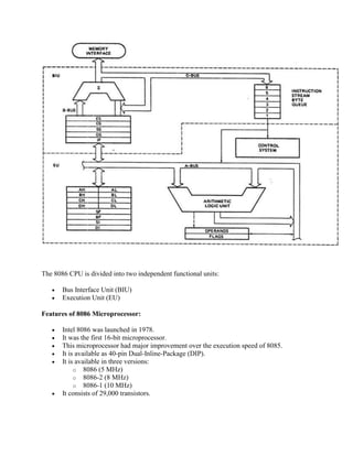
  • 1. The 8086 CPU is divided into two independent functional units:  Bus Interface Unit (BIU)  Execution Unit (EU) Features of 8086 Microprocessor:  Intel 8086 was launched in 1978.  It was the first 16-bit microprocessor.  This microprocessor had major improvement over the execution speed of 8085.  It is available as 40-pin Dual-Inline-Package (DIP).  It is available in three versions: o 8086 (5 MHz) o 8086-2 (8 MHz) o 8086-1 (10 MHz)  It consists of 29,000 transistors.
  • 2. Bus Interface Unit (BIU) The function of BIU is to:  Fetch the instruction or data from memory.  Write the data to memory.  Write the data to the port.  Read data from the port.  Instruction Queue 1. To increase the execution speed, BIU fetches as many as six instruction bytes ahead to time from memory. 2. All six bytes are then held in first in first out 6 byte register called instruction queue. 3. Then all bytes have to be given to EU one by one. 4. This pre fetching operation of BIU may be in parallel with execution operation of EU, which improves the speed execution of the instruction. 5. Execution Unit (EU) The functions of execution unit are:  To tell BIU where to fetch the instructions or data from.  To decode the instructions.  To execute the instructions. The EU contains the control circuitry to perform various internal operations. A decoder in EU decodes the instruction fetched memory to generate different internal or external control signals required to perform the operation. EU has 16-bit ALU, which can perform arithmetic and logical operations on 8-bit as well as 16-bit. General Purpose Registers of 8086 These registers can be used as 8-bit registers individually or can be used as 16-bit in pair to have AX, BX, CX, and DX. 1. AX Register: AX register is also known as accumulator register that stores operands for arithmetic operation like divided, rotate. 2. BX Register: This register is mainly used as a base register. It holds the starting base location of a memory region within a data segment. 3. CX Register: It is defined as a counter. It is primarily used in loop instruction to store loop counter. 4. DX Register: DX register is used to contain I/O port address for I/O instruction.
  • 3. Segment Registers Additional registers called segment registers generate memory address when combined with other in the microprocessor. In 8086 microprocessor, memory is divided into 4 segments. 1. Code Segment (CS): The CS register is used for addressing a memory location in the Code Segment of the memory, where the executable program is stored. 2. Data Segment (DS): The DS contains most data used by program. Data are accessed in the Data Segment by an offset address or the content of other register that holds the offset address. 3. Stack Segment (SS): SS defined the area of memory used for the stack. 4. Extra Segment (ES): ES is additional data segment that is used by some of the string to hold the destination data. Flag Registers of 8086 Fig. 3: Flag Register of 8086 Flags Register determines the current state of the processor. They are modified automatically by CPU after mathematical operations, this allows to determine the type of the result, and to determine conditions to transfer control to other parts of the program. 8086 has 9 flags and they are divided into two categories: 1. Conditional Flags 2. Control Flags Conditional Flags Conditional flags represent result of last arithmetic or logical instruction executed. Conditional flags are as follows:  Carry Flag (CF): This flag indicates an overflow condition for unsigned integer arithmetic. It is also used in multiple-precision arithmetic.  Auxiliary Flag (AF): If an operation performed in ALU generates a carry/barrow from lower nibble (i.e. D0 – D3) to upper nibble (i.e. D4 – D7), the AF flag is set i.e. carry given by D3 bit to D4 is AF flag. This is not a general-purpose flag, it is used internally by the processor to perform Binary to BCD conversion.
  • 4.  Parity Flag (PF): This flag is used to indicate the parity of result. If lower order 8-bits of the result contains even number of 1’s, the Parity Flag is set and for odd number of 1’s, the Parity Flag is reset.  Zero Flag (ZF): It is set; if the result of arithmetic or logical operation is zero else it is reset.  Sign Flag (SF): In sign magnitude format the sign of number is indicated by MSB bit. If the result of operation is negative, sign flag is set.  Overflow Flag (OF): It occurs when signed numbers are added or subtracted. An OF indicates that the result has exceeded the capacity of machine. Control Flags Control flags are set or reset deliberately to control the operations of the execution unit. Control flags are as follows: 1. Trap Flag (TP): a. It is used for single step control. b. It allows user to execute one instruction of a program at a time for debugging. c. When trap flag is set, program can be run in single step mode. 2. Interrupt Flag (IF): a. It is an interrupt enable/disable flag. b. If it is set, the maskable interrupt of 8086 is enabled and if it is reset, the interrupt is disabled. c. It can be set by executing instruction sit and can be cleared by executing CLI instruction. 3. Direction Flag (DF): a. It is used in string operation. b. If it is set, string bytes are accessed from higher memory address to lower memory address. c. When it is reset, the string bytes are accessed from lower memory address to higher memory address.
  • 5. 8086/88 Device Specifications  Both are packaged in DIP (Dual In-Line Packages).  8086: 16-bit microprocessor with a 16-bit data bus  8088: 16-bit microprocessor with an 8-bit data bus.  Both are 5V parts:  8086: Draws a maximum supply current of 360mA.  8086: Draws a maximum supply current of 340mA.  80C86/80C88: CMOS version draws 10mA with temp spec -40 to 225degF.  Input/Output current levels: o Yields a 350mV noise immunity for logic 0 (Output max can be as high as 450mV while input max can be no higher than 800mV). o This limits the loading on the outputs. 8086/88 Pinout
  • 6. 8086/88 Pinout  Pin functions:  AD15-AD0 o Multiplexed address(ALE=1)/data bus(ALE=0).  A19/S6-A16/S3 (multiplexed) o High order 4 bits of the 20-bit address OR status bits S6-S3.  M/IO o Indicates if address is a Memory or IO address.  RD o When 0, data bus is driven by memory or an I/O device.  WR o Microprocessor is driving data bus to memory or an I/O device. When 0, data bus contains valid data.  ALE (Address latch enable) o When 1, address data bus contains a memory or I/O address.  DT/R (Data Transmit/Receive) o Data bus is transmitting/receiving data.  DEN (Data bus Enable) o Activates external data bus buffers. 8086/88 Pinout  Pin functions:  S7, S6, S5, S4, S3, S2, S1, S0 o S7: Logic 1, S6: Logic 0. o S5: Indicates condition of IF flag bits. o S4-S3: Indicate which segment is accessed during current bus cycle:
  • 7. o S2, S1, S0 : Indicate function of current bus cycle (decoded by 8288). 8086/88 Pinout  Pin functions:  INTR o When 1 and IF=1, microprocessor prepares to service interrupt. INTA becomes active after current instruction completes.  INTA o Interrupt Acknowledge generated by the microprocessor in response to INTR. Causes the interrupt vector to be put onto the data bus.  NMI o Non-maskable interrupt. Similar to INTR except IF flag bit is not consulted and interrupt is vector 2.  CLK o Clock input must have a duty cycle of 33% (high for 1/3 and low for 2/3s)  VCC/GND o Power supply (5V) and GND (0V). 8086/88 Pinout  Pin functions:  MN/ MX o Select minimum (5V) or maximum mode (0V) of operation.  BHE o Bus High Enable. Enables the most significant data bus bits (D 15 -D 8 ) during a read or write operation.  READY o Used to insert wait states (controlled by memory and IO for reads/writes) into the microprocessor.  RESET o Microprocessor resets if this pin is held high for 4 clock periods.
  • 8. o Instruction execution begins at FFFF0H and IF flag is cleared.  TEST o An input that is tested by the WAIT instruction. o Commonly connected to the 8087 coprocessor. 8086/88 Pinout  Pin functions:  HOLD o Requests a direct memory access (DMA). When 1, microprocessor stops and places address, data and control bus in high-impedance state.  HLDA (Hold Acknowledge) o Indicates that the microprocessor has entered the hold state.  RO/GT1 and RO/GT0 o Request/grant pins request/grant direct memory accesses (DMA) during maximum mode operation.  LOCK o Lock output is used to lock peripherals off the system. Activated by using the LOCK: prefix on any instruction.  QS1 and QS0 o The queue status bits show status of internal instruction queue. Provided for access by the numeric coprocessor (8087). 8284A Clock Generator  Basic functions:  Clock generation.  RESET synchronization.  READY synchronization.  Peripheral clock signal.  Connection of the 8284 and the 8086.
  • 9. 8284A Clock Generator 8284A Clock Generator  Clock generation: o Crystal is connected to X1 and X2. o XTAL OSC generates square wave signal at crystal's frequency which feeds:  An inverting buffer (output OSC) which is used to drive the EFI input of other 8284As.  2-to-1 MUX  F/ C selects XTAL or EFI external input. o The MUX drives a divide-by-3 counter (15MHz to 5MHz). o This drives:  The READY flipflop (READY synchronization).  A second divide-by-2 counter (2.5MHz clk for peripheral components).  The RESET flipflop.  CLK which drives the 8086 CLK input. 8284A Clock Generator  RESET: o Negative edge-triggered flipflop applies the RESET signal to the 8086 on the falling edge. o The 8086 samples the RESET pin on the rising edge.
  • 10. o Correct reset timing requires that the RESET input to the microprocessor becomes a logic 1 NO LATER than 4 clocks after power up and stay high for at least 50us. BUS Buffering and Latching  Demultiplexing the Buses: o Computer systems have three buses:  Address  Data  Control o The Address and Data bus are multiplexed (shared) due to pin limitations on the 8086.  The ALE pin controls a set of latches. o All signals MUST be buffered.  Latches buffer for A 0 -A 15 .  Control and A 16 -A 19 + BHE are buffered separately.  Data bus buffers must be bi-directional buffers (BB). o BHE : Selects the high-order memory bank. BUS Buffering and Latching
  • 11. BUS Timing  Writing:  Dump address on address bus.  Dump data on data bus.  Issue a write ( WR ) and set M/ IO to 1. BUS Timing  Reading:  Dump address on address bus.  Issue a read ( RD ) and set M/ IO to 1.  Wait for memory access cycle. BUS Timing  Bus Timing: BUS Timing  During T 1 :  The address is placed on the Address/Data bus.
  • 12.  Control signals M/ IO , ALE and DT/ R specify memory or I/O, latch the address onto the address bus and set the direction of data transfer on data bus.  During T 2 :  8086 issues the RD or WR signal, DEN , and, for a write, the data.  DEN enables the memory or I/O device to receive the data for writes and the 8086 to receive the data for reads.  During T 3 :  This cycle is provided to allow memory to access data.  READY is sampled at the end of T 2 .  If low, T 3 becomes a wait state.  Otherwise, the data bus is sampled at the end of T 3 .  During T 4 :  All bus signals are deactivated, in preparation for next bus cycle.  Data is sampled for reads, writes occur for writes. BUS Timing  Timing: o Each BUS CYCLE on the 8086 equals four system clocking periods (T states). o The clock rate is 5MHz , therefore one Bus Cycle is 800ns . o The transfer rate is 1.25MHz . o Memory specs (memory access time) must match constraints of system timing. o For example, bus timing for a read operation shows almost 600ns are needed to read data.  However, memory must access faster due to setup times, e.g. Address setup and data setup.  This subtracts off about 150ns .  Therefore, memory must access in at least 450ns minus another 30-40ns guard band for buffers and decoders.  420ns DRAM required for the 8086. BUS Timing  READY: o An input to the 8086 that causes wait states for slower memory and I/O components.
  • 13. o A wait state (T W ) is an extra clock period inserted between T 2 and T 3 to lengthen the bus cycle.  For example, this extends a 460ns bus cycle (at 5MHz clock) to 660ns . o Text discusses role of 8284A and timing requirements for the 8086. MIN and MAX Mode  Controlled through the MN/ MX pin.  Minimum mode is cheaper since all control signals for memory and I/O are generated by the microprocessor.  Maximum mode is designed to be used when a coprocessor (8087) exists in the system.  Some of the control signals must be generated externally, due to redefinition of certain control pins on the 8086. o The following pins are lost when the 8086 operates in Maximum mode .  ALE  WR  IO/ M  DT/ R  DEN  INTA  This requires an external bus controller: The 8288 Bus Controller . 8288 Bus Controller
  • 14.  Separate signals are used for I/O ( IORC and IOWC ) and memory ( MRDC and MWTC ).  Also provided are advanced memory ( AIOWC ) and I/O ( AIOWC ) write strobes plus INTA . MAX Mode 8086 System