Programmable Logic Controller | Ladder Logic diagrams| Block diagram | I/O Module | Programming
•Download as PPTX, PDF•
0 likes•377 views

Programmable Logic Controller | Ladder Logic diagrams| Block diagram | I/O Module | Programming

Recommended
More Related Content
What's hot
What's hot (20)
Similar to Programmable Logic Controller | Ladder Logic diagrams| Block diagram | I/O Module | Programming
Similar to Programmable Logic Controller | Ladder Logic diagrams| Block diagram | I/O Module | Programming (20)
More from Waqas Afzal
More from Waqas Afzal (20)
Recently uploaded
Recently uploaded (20)
Programmable Logic Controller | Ladder Logic diagrams| Block diagram | I/O Module | Programming
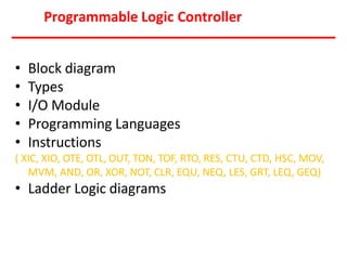
- 1. Programmable Logic Controller • Block diagram • Types • I/O Module • Programming Languages • Instructions ( XIC, XIO, OTE, OTL, OUT, TON, TOF, RTO, RES, CTU, CTD, HSC, MOV, MVM, AND, OR, XOR, NOT, CLR, EQU, NEQ, LES, GRT, LEQ, GEQ) • Ladder Logic diagrams
- 2. What is a Programmable Logic Controller? A programmable logic controller (PLC) is a digital computer used for automation of electromechanical processes, such as control of machinery on factory assembly lines, amusement rides, or lighting fixtures. PLCs are used in many industries and machines.
- 3. (Definition according to NEMA standard ICS3-1978) A digitally operating electronic apparatus which uses a programming memory for the internal storage of instructions for implementing specific functions such as logic, sequencing, timing, counting and arithmetic to control through digital or analog modules, various types of machines or process. Definition of PLC
- 4. Block Diagram of PLC
- 5. I/O Section Input Module Forms the interface by which input field devices are connected to the controller. The terms “field” and “real world” are used to distinguish actual external devices that exist and must be physically wired into the system. 5
- 6. I/O Section Output Module Forms the interface by which output field devices are connected to the controller. PLCs employ an optical isolator which uses light to electrically isolate the internal components from the input and output terminals.
- 7. Programming Device PC with appropriate software A personal computer (PC) is the most commonly used programming device. The personal computer communicates with the PLC processor via a serial or parallel data communications link. The computer monitor is used to display the logic on the screen.
- 10. Types of PLC Fixed PLC: A Fixed PLC has all of its components-the input section, supply, CPU and associated memory, power and output section-built into one self- contained unit. All input and output terminals are built into the PLC package and are fixed, not removable.
- 11. Types of PLC Modular PLC: The modular PLC comes as separate pieces. A modular PLC is purchased piece by piece. There may be two or three power supplies to choose from, a handful of different processors (CPUs), many separate input and output cards or modules, and selection of assemblies, called racks, chassis, or base plates to hold the pieces together.
- 12. Block diagram of AC input module Bridge Rectifier Noise & Debounce Filter Threshold Detector Optical Isolation Logic CPU LED Input Status Table Input Signal
- 13. AC Input Module Specifications Points per common: This is the number of input points that share the same common connection. As an example, one 16 point input module could have all input points sharing one common, and a different 16 point input module might have two groups of 8 input points. Each group of 8 would have its own separate common.
- 14. AC Input Module Specifications Backplane Current Draw: Each module takes power from the PLCs power supply to operate the electronics on the module. This specification will be used when calculating power supply loading. Maximum signal delay: Signal delay is the time it takes for the PLC to pick up the field input signal, digitize it, and store it in the memory. This specification is usually listed for signal turning on and for a signal turning off.
- 15. AC Input Module Specifications Nominal input current: this is the current drawn by an input point at nominal input voltage. Maximum Inrush Current: this is the maximum inrush current the module can handle. Maximum off state current: this is the maximum amount of current, typically from leakage from a solid state input device, that a module can accept while remaining in an OFF state.
- 16. Block diagram of DC input module Power Conversion Noise & Debounce Filter Threshold Detector Optical Isolation Logic CPU LED Input Status Table Input Signal + -
- 17. DC Input Module Specifications Maximum Off state current: This is the maximum amount of leakage current allowed in an input circuit from an input device that will keep the input circuit in an OFF state.
- 18. Block diagram of AC output Module Latch Logic Circuit Triac Switching Circuit Optical Isolation Filter Controlled Device Fuse Signal From CPU LED
- 19. Block diagram of DC output module Latch Logic Circuit Power Transistor Switching Circuit Optical Isolation Filter Controlled Device Fuse Signal From CPU LED
- 20. Programming Languages Ladder Diagram (LD):a graphical depiction of a process with rungs of logic, similar to the relay ladder logic schemes that were replaced by PLCs. Sequential Function Charts (SFC): a graphical depiction of interconnecting steps, actions, and transitions. Instruction List (IL): assembler type, text based language for building small applications or optimizing complex systems.
- 21. Programming Languages Function Block Diagram (FBD): a graphical depiction of process flow using simple and complex interconnecting blocks. Structured Text (ST): a high-level, text-based language such as BASIC, C, or PASCAL specifically developed for industrial control applications.
- 22. PLC Ladder Programming A very commonly used method of programming PLCs is based on the use of ladder diagrams. Writing a program is then equivalent to drawing a switching circuit. The ladder diagram consists of two vertical lines representing the power rails. Circuits are connected as horizontal lines, that is, the rungs of the ladder, between these two verticals.
- 23. Relay Type Instructions Sr. No. Instruction Description 1 XIC Examine if closed 2 XIO Examine if open 3 OTE Output Energize 4 OTL Output Latch 5 OTU Output Unlatch
- 24. Fundamental Symbols Figure : Relay Contact Figure : Relay Contact Figure : Relay Coil Examine If Closed (XIC) Examine If Open (XIO) Output Energize (OTE)
- 25. OTL and OTU Instructions Instruction Name Symbol Description OTL Output Latch L OTL sets the bit to "1" when the rung becomes true and retains its state when the rung loses continuity or a power cycle occurs. OTU Output Unlatch U OTU resets the bit to "0" when the rung becomes true and retains it.
- 26. Timer Instructions Sr. No. Instruction Name Description 1 TON On Delay Timer Counts time-based intervals when the instruction is true. 2 TOF Off Delay Timer Counts time-based intervals when the instruction is false. 3 RTO Retentive Timer Counts time-based intervals when the instruction is true and retains the accumulated value when the instruction goes false or when power cycle occurs. 4 RES Reset Resets a retentive timer’s accumulated value to zero.
- 27. On Delay Timer Sequence Input Timer Rung Condition Time Period Timed Output Bit False True On Delay Timed Duration True False On (Logic 1) Off (Logic 0) Preset Value= Accumulated Value
- 28. TON – On Delay Timer Instruction TON EN DN TIMER ON DELAY Timer Time Base Preset Accumulated T4:0 1:0 15 0 The On delay timer operates such that when the rung containing timer is true, the timer timed out period commences. At the end of the timer time out period, an output is made active.
- 29. Timer number —This number must come from the timer file. In the example shown, the timer number is T4:0, which represents timer file 4, timer 0 in that file. The timer address must be unique for this timer and may not be used for any other timer. Time base —The time base (which is always expressed in seconds) may be either 1.0 s or 0.01 s. In the example shown, the time base is 1.0 s. Preset value —In the example shown, the preset value is 15. The timer preset value can range from 0 through 32,767. Accumulated value —In the example shown, the accumulated value is 0. The timer’s accumulated value normally is entered as 0, although it is possible to enter a value from 0 through 32,767. Regardless of the value that is preloaded, the timer value will become 0 whenever the timer is reset. TON – On Delay Timer Instruction
- 30. Off Delay Timer Sequence Input Timer Rung Condition Timed Period Timed Output Bit False True Off Delay Timed Duration True False On (Logic 1) Off (Logic 0) Preset Value= Accumulated Value
- 31. TOF – Off Delay Timer Instruction TOF EN DN TIMER OFF DELAY Timer Time Base Preset Accumulated T4:0 1:0 15 0 The Off delay timer operation will keep the output energized for a time period after the rung containing the timer has gone false.
- 32. RTO – Retentive Timer A retentive timer accumulates time whenever the device receives power, and it maintains the current time should power be removed from the device. Once the device accumulates time equal to its preset value, the contacts of the device change state. RTO EN DN RETENTIVE TIMER ON Timer Time Base Preset Accumulated T4:0 1:0 15 0
- 33. RTO – Timer Programmed Logic RTO EN DN RETENTIVE TIMER ON Timer Time Base Preset Accumulated T4:0 1:0 7 0 PB1 T4:2 PL DN
- 34. RTO – Timer Sequence 0 2 1 3 4 5 6 7 Time Input Timer T4:2 Enable Bit Accumulated Value Accumulated Value retained When rung condition goes false Acc Value = Pre Value Timer T4:2 Done Bit PL Output False True On Off On Off On Off
- 35. RES – Reset Instruction Because the retentive timer does not reset to 0 when the timer is de-energized, the reset instruction RES must be used to reset the timer. The RES instruction given the same address (T4:2) as the RTO. When reset pushbutton closes, RES resets the accumulated time to 0 and DN bit to 0, turning output off. Reset RES T4:2
- 36. Counter Instructions Sr. No. Instruction Name Description 1 CTU Up counter Increments the accumulated value at each false-to-true transition and retains the accumulated value when an off/on power cycle occurs. 2 CTD Down counter Decrements the accumulated value at each false-to-true transition and retains the accumulated value when an on/off power cycle occurs. 3 HSC High Speed Counter Counts high-speed pulses from a high- speed input. 4 RES Reset Resets a counter’s accumulated value to zero.
- 37. UP Counter Counting Sequence Limit Switch Counter UP Counter Value +4 Accumulated Value= preset = output OFF ON
- 38. CTU – Up Counter Instruction CTU CU DN COUNT – UP COUNTER Counter Preset Accumulated C5:0 7 0 RES C5:0/CU C5:0/DN C5:0/OV C5:0 Counter Enable Bit Counter Done Bit Overflow Status Bit Counter Reset Instruction
- 39. CTU – Up Counter Sequence Count Up Input DN Bit of Counter Reset Accumulated Value 1 PRE Value =7 7 6 5 4 3 2 5 6 7 TRUE 1 2 3 4 FALSE
- 40. CTU – UP Counter Instruction Counter Number —This number must come from the counter fi le. In the example shown, the counter number is C5:0, which represents counter file 5, counter 0 in that file. The address for this counter should not be used for any other count-up counter. Preset Value —The preset value can range from 232,768 to 132,767. In the example shown, the preset value is 10. Accumulated Value —The accumulated value can also range from 232,768 through 132,767. Typically, as in this example, the value entered in the accumulated word is 0. Regardless of what value is entered, the reset instruction will reset the accumulated value to 0.
- 41. CTU – UP Counter Instruction Control Word C5:N Bit 15 14 13 12 11 10 09 08 07 06 05 04 03 02 01 00 C5:N:0 Word 0 CU CD DN OV UN UA INTERNAL USE (not addressable) C5:N:1 Word 1 PRESET VALUE C5:N:2 Word 2 ACCUMULATED VALUE
- 42. CTU – UP Counter Instruction Control Word Count-Up (CU) Enable Bit —The count-up enable bit is used with the count-up counter and is true whenever the count-up counter instruction is true. If the count- up counter instruction is false, the CU bit is false. Done (DN) Bit —The done bit is true whenever the accumulated value is equal to or greater than the preset value of the counter, for either the count-up or the count-down counter.
- 43. Overflow (OV) Bit —The overflow bit is true whenever the counter counts past its maximum value, which is 32,767. On the next count, the counter will wrap around to 32,768 and will continue counting from there toward 0 on successive false-to- true transitions of the count-up counter. Update Accumulator (UA) Bit —The update accumulator bit is used only in conjunction with an external HSC (high-speed counter). CTU – UP Counter Instruction Control Word
- 44. DOWN Counter Counting Sequence Proximity Switch Counter Down Counter Value -5 Accumulated Value= Preset = output OFF ON
- 45. CTD – Down Counter Instruction CTD CD DN COUNT – DOWNCOUNTER Counter Preset Accumulated C5:0 7 0 RES C5:0/CD C5:0/DN C5:0/UN C5:0 Counter Enable Bit Counter Done Bit Underflow Status Bit Counter Reset Instruction
- 46. CTD – Down Counter Sequence Count Down Input Accumulated Value DN Bit of Counter Reset 7 6 5 4 3 2 1 PRE Value 5 6 7 TRUE 1 2 3 4 FALSE
- 47. CTD – Down Counter Instruction Counter Number —This number must come from the counter fi le. In the example shown, the counter number is C5:0, which represents counter file 5, counter 0 in that file. The address for this counter should not be used for any other count-up counter. Preset Value —The preset value can range from 232,768 to 132,767. In the example shown, the preset value is 10. Accumulated Value —The accumulated value can also range from 232,768 through 132,767. Typically, as in this example, the value entered in the accumulated word is 0. Regardless of what value is entered, the reset instruction will reset the accumulated value to 0.
- 48. CTD – Down Counter Instruction Control Word C5:N Bit 15 14 13 12 11 10 09 08 07 06 05 04 03 02 01 00 C5:N:0 Word 0 CU CD DN OV UN UA INTERNAL USE (not addressable) C5:N:1 Word 1 PRESET VALUE C5:N:2 Word 2 ACCUMULATED VALUE
- 49. Count-Down (CD) Enable Bit —The count-down enable bit is used with the count-down counter and is true whenever the count-down counter instruction is true. If the count- down counter instruction is false, the CD bit is false. Done (DN) Bit —The done bit is true whenever the accumulated value is equal to or greater than the preset value of the counter, for either the count-up or the count- down counter. CTU – UP Counter Instruction Control Word
- 50. CTU – UP Counter Instruction Control Word Underflow (UN) Bit —The underflow bit will go true when the counter counts below 32,768. The counter will wrap around to 132,767 and continue counting down toward 0 on successive false-to-true rung transitions of the count-down counter. Update Accumulator (UA) Bit —The update accumulator bit is used only in conjunction with an external HSC (high-speed counter).
- 51. Data Handling Instructions Sr. No. Instruction Name Description 1 MOV Move Moves the source value to the destination. 2 MVM Masked Move Moves data from a source location to a selected portion of the destination.
- 52. MOV Instruction When the rung is true, input switch A closed, the value stored at the source address, N7:30, is copied into the destination address, N7:20. When the rung goes false, input switch A opened, the destination address will retain the value unless it is changed elsewhere in the program. The source value remains unchanged and no data conversion occurs. MOV MOVE Source Destination N7:30 N7:20 PB1 N7:30 N7:20
- 53. MVM Instruction The move with mask (MVM) instruction differs slightly from the MOV instruction because a mask word is involved in the move. The data being moved must pass through the mask to get to their destination address. Masking refers to the action of hiding a portion of a binary word before transferring it to the destination address.
- 54. MVM Instruction The pattern of characters in the mask determines which source bits will be passed through to the destination address. The bits in the mask that are set to zero (0) do not pass data. Only the bits in the mask that are set to one (1) will pass the source data through to the destination. Bits in the destination are not affected when the corresponding bits in the mask are zero. The MVM instruction is used to copy the desired part of a 16-bit word by masking the rest of the value. MVM B3:0 MASKED MOVE Source 1010101010101010 Mask B3:1 FF0F B3:4 Destination 1010101011001010
- 55. MVM Instruction MVM B3:0 MASKED MOVE Source 1010101010101010 Mask B3:1 FF0F B3:4 Destination 1010101011001010 PB1 1 0 1 0 1 0 1 0 1 0 1 0 1 0 1 0 1 1 1 1 1 1 1 1 0 0 0 0 1 1 1 1 1 1 0 0 1 1 0 0 1 1 0 0 1 1 0 0 1 0 1 0 1 0 1 0 1 1 0 0 1 0 1 0 Source B3:0 Mask FF0F Destination B3:4 before instruction went true Destination B3:4 after instruction went true
- 56. Logical Instructions Sr. No. Instruction Name Description 1 AND Logical AND Perform operation Bitwise AND 2 OR Logical OR Perform operation Bitwise OR 3 XOR Logical XOR Perform operation Bitwise XOR
- 57. Logical Instructions Sr. No. Instruction Name Description 4 NOT Inversion Perform inversion of given source 5 CLR Clear Clear destination
- 58. AND – Logical AND Instruction AND B3:0 Destination B3:2 The AND command is used to perform the logic AND instruction on each bit of the value in source A with each bit of the value of source B, storing the output logic in the destination. B3:1 BITWISE AND Source A Source B B3:0 0 0 0 0 0 0 0 0 0 0 1 0 1 0 1 0 B3:1 0 0 0 0 0 0 0 0 0 0 1 1 1 1 1 0 B3:2 0 0 0 0 0 0 0 0 0 0 1 0 1 0 1 0
- 59. OR – Logical OR Instruction OR B3:0 Destination B3:2 The OR command is used to perform the logic OR instruction on each bit of the value in source A with each bit of the value of source B, storing the output logic in the destination. B3:1 BITWISE INCLUSIVEOR Source A Source B B3:0 0 0 0 0 0 0 0 0 0 0 1 0 1 0 1 0 B3:1 0 0 0 0 0 0 0 0 0 0 1 1 1 1 1 0 B3:2 0 0 0 0 0 0 0 0 0 0 1 1 1 1 1 0
- 60. XOR – Logical XOR Instruction XOR B3:0 Destination B3:2 The XOR command is used to perform the logic XOR instruction on each bit of the value in source A with each bit of the value of source B, storing the output logic in the destination. B3:1 BITWISE EXCLUSIVEOR Source A Source B B3:0 0 0 0 0 0 0 0 0 0 0 1 0 1 0 1 0 B3:1 0 0 0 0 0 0 0 0 0 0 1 1 1 1 1 0 B3:2 0 0 0 0 0 0 0 0 0 0 0 1 0 1 0 0
- 61. NOT – Inversion Instruction NOT NOT Source B3:0 Destination B3:1 The NOT instruction is used to perform the NOT logic on the value in the source, bit by bit. The output logic value returned in the destination is the one's complement or opposite of the value in the source. B3:0 0 0 0 0 0 0 0 0 0 0 1 0 1 0 1 0 B3:1 1 1 1 1 1 1 1 1 1 1 0 1 0 1 0 1
- 62. CLR – Clear Instruction The CLR instruction is used to set the destination value of a word to zero. CLR CLEAR Destination B3:1 0 0 0 0 0 0 0 0 0 0 0 0 0 0 0 0 B3:1
- 63. XIC, XIO, OTE, OTL, OUT, TON, TOF, RTO, RES, CTU, CTD, HSC, MOV, MVM, AND, OR, XOR, NOT, CLR, EQU, NEQ, LES, GRT, LEQ, GEQ,
- 64. Data Compare Instructions Sr. No. Instruction Name Description 1 EQU Equal Tests whether two values are equal. 2 NEQ Not Equal Tests whether one value is not equal to a second value. 3 LES Less Than Tests whether one value is less than a second value.
- 65. Data Compare Instructions Sr. No. Instruction Name Description 4 GRT Greater Than Tests whether one value is greater than a second value. 5 LEQ Less Than or Equal Tests whether one value is less than or equal to a second value. 6 GEQ Greater Than or Equal Tests whether one value is greater than or equal to a second value.
- 66. EQU – Equal Instruction EQU EQUAL Source A T4:0.ACC Source B N7:40 The equal (EQU) instruction is an input instruction that compares source A to source B: when source A is equal to source B, the instruction is logically true; otherwise it is logically false.
- 67. NEQ – Not Equal Instruction NEQ NOT EQUAL Source A N7:5 Source B 25 The not equal (NEQ) instruction is an input instruction that compares source A to source B: when source A is not equal to source B, the instruction is logically true; otherwise it is logically false.
- 68. GRT – Greater Than Instruction The greater than (GRT) instruction is an input instruction that compares source A to source B: when source A is greater than source B, the instruction is logically true; otherwise it is logically false. GRT GREATER THAN Source A Source B T4:0.ACC 200
- 69. LES – Less Than Instruction LES LESS THAN Source A C5:10.ACC Source B 350 The less than (LES) instruction is an input instruction that compares source A to source B: when source A is less than source B, the instruction is logically true; otherwise it is logically false.
- 70. GEQ – Greater Than or Equal Instruction The greater than or equal (GEQ) instruction is an input instruction that compares source A to source B: when source A is greater than or equal to source B, the instruction is logically true; otherwise it is logically false. Source B GEQ GREATER THAN OR EQUAL Source A N7:55 N7:12
- 71. LEQ – Less Than or Equal Instruction LEQ LESS THAN OR EQUAL Source A C5:1.ACC Source B 457 The less than or equal (LEQ) instruction is an input instruction that compares source A to source B: when source A is less than or equal to source B, the instruction is logically true; otherwise it is logically false.
- 72. Ladder Diagram for AND Gate Input Input A B Output Input B Output Applied Voltage (a) Input A (b) (c)
- 73. Ladder Diagram for OR Gate B Applied Voltage Input A Input B Output Input A Input B Output Input B Output Input A (a) (b) (c) (d)
- 74. Ladder Diagram for NOT Gate A Applied Voltage (a) Input A Output Input A Output (b) (c)
- 75. Ladder Diagram for NAND Gate Input A Input B Output Input A Input B Output (a) (b)
- 76. Ladder Diagram for NOR Gate Input A Input B Output Input A Input B Output (a) (b)
- 77. Ladder Diagram for Ex-OR Gate t A Input B Output Input A Input B Output Inpu Input A Input B (a) (b)
- 78. Ladder Diagram for Ex-NOR Gate t A Input B Output Input A Input B Output Inpu Input A Input B (a) (b)
- 79. Example 1 Draw Ladder diagram for given logic diagram A B C Y A C Y B
- 80. Example 2 Draw Ladder diagram for given logic diagram A B C D Y A C Y B D
- 81. Example 3 Draw Ladder diagram for given logic diagram A B C Y A B Y C
- 82. Example 4 Draw Ladder diagram for given logic diagram A B Y A B Y C C D D
- 83. Example 7 Draw Ladder diagram for given Boolean Expression Y A B C D A B Y C D
- 84. Example 14 Draw Ladder diagram for given Boolean Expression Y A ( B C ) B ( A C ) B A Y A B C C
- 85. Example 21 Draw Ladder diagram to switch off three motors sequentially at 5 seconds interval
- 86. EN DN TIMER OFFDELAY Timer TimeBase Preset Accumulated T4:1 1:0 5 0 TOF EN DN TIMER OFFDELAY Timer TimeBase Preset Accumulated T4:2 1:0 10 0 TOF EN DN TIMER OFFDELAY Timer TimeBase Preset Accumulated T4:3 1:0 15 0 TOF SW T4:1/DN T4:2/DN T4:3/DN M1 M2 M3
- 87. Example 22 Draw Ladder diagram for 2 motor operations for following conditions 1. Start push button starts motors M1 and M2 2. Stop push button stop motors M1 first and after 10 sec motor M2
- 88. EN DN TIMER OFF DELAY Timer Time Base Preset Accumulated T4:1 1:0 10 0 TOF Start T4:1/DN M2 Example 22 M1 I:0/0 Stop I:0/1 O:0/0 O:0/0 O:0/1