BSides Seattle 2024 - Stopping Ethan Hunt From Taking Your Data.pptx
Numerical Exercise on JFET/MOSFET
1. Numerical Exercise on JFET/MOSFET
Dr. Varun Kumar
*************************************************************************************
FET Biasing
Fixed Bias Configuration
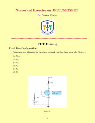
1. Determine the following for the given network that has been shown in Figure 1.
(a) VGSQ
(b) IDQ
(c) VDS
(d) VD
(e) VG
(f) VS
Figure 1:
1
2. 2. The amplifier of Figure 2 utilizes n-channel FET for which VP = −2V and IDSS =
1.65mA. It is desired to bias the circuit at ID = 0.8mA, using VDD = 24V . Assume
rd >> Rd. Find
(a) gm
(b) VGS
(c) Rs
(d) Rd
Figure 2:
such that the voltage gain is at least 20 dB, with Rs bypassed with a very large
capacitance Cs.
Voltage Divider Biasing
3. Determine the following for the given network that has been shown in Figure 3.
(a) IDQ and VGSQ
(b) VD
(c) VS
(d) VDS
(e) VDG
2
3. Figure 3:
Design and Troubleshoothing
Figure 4:
4. A network that has been shown in Figure 4, the levels of VDQ and IDQ are specified.
Determine the required value of RD and RS. What are the closest commercial
value.
3
4. FET Amplifier Network
5. Choose the value of RD and RS for the network shown in Figure 5. The voltage
gain of the given FET is 8. A relatively high level of gm for this device defined
at VGSQ = VP
4
Figure 5:
Cascade Connection
6. A cascade connected electrical network has been shown in Figure 6. What will
be the output voltage.
Figure 6:
4