![LAYOUTFOR CASCODESTAGEOF TWO NMOS IN LNA:
PARASITIC RESISTANCECALCULATION:
Rpoly= 7 ohm/sq, RM1 =0.0709 ohm/sq , RM2,3 =0.0639 ohm/sq
Width of each NMOS = WNFET = 40um
Number of fingers = NF = 40
Width of each finger = WF = 1um
Length of each finger = LF = 0.12um
Widths of gate around the contact : WPCONT = 0.2um, Wp = 0.4um
Width of external gate between transistor and contact = Wext = 0.08um
Lp = 18.84um
Npcont = Lp/Wp = 47
Wcont = 0.16um
Rgp =
1
𝑁 𝑓
[
𝑊 𝑓𝑖𝑛𝑔𝑒𝑟
12∗𝐿
𝑅 𝑝𝑜𝑙𝑦 +
𝑊 𝑓𝑖𝑛𝑔𝑒𝑟
2∗𝐿
𝑅 𝑝𝑜𝑙𝑦 + (
𝑊 𝑓𝑖𝑛𝑔𝑒𝑟
𝑊 𝑝
+ 0.5)
𝑅 𝑝𝑜𝑙𝑦
2
]
Rgp =
1
40
[
1𝑢𝑚
12∗0.13𝑢𝑚
7 +
0.08
2∗0.12𝑢𝑚
7 + (
0.2
0.4
+ 0.5)
7
2
]](data:image/gif;base64,R0lGODlhAQABAIAAAAAAAP///yH5BAEAAAAALAAAAAABAAEAAAIBRAA7)
Recommended
Recommended
More Related Content
What's hot
What's hot (19)
Similar to PARASITICS REDUCTION FOR RFIC CMOS LAYOUT AND IIP3 VS Q-BASED DESIGN ANALYSIS USING IBM 130NM TECHNOLOGY
Similar to PARASITICS REDUCTION FOR RFIC CMOS LAYOUT AND IIP3 VS Q-BASED DESIGN ANALYSIS USING IBM 130NM TECHNOLOGY (20)
Recently uploaded
Recently uploaded (20)
PARASITICS REDUCTION FOR RFIC CMOS LAYOUT AND IIP3 VS Q-BASED DESIGN ANALYSIS USING IBM 130NM TECHNOLOGY
- 1. THE UNIVERSITY OF TEXAS AT DALLAS ERIK JONSSON SCHOOL OF ENGINEERING & COMPUTER SCIENCE EERF 6330 RFIC DESIGN Kenneth O. SPRING 2016 PARASITICS REDUCTION FOR RFIC CMOS LAYOUT AND IIP3 VS Q-BASED DESIGN ANALYSIS USING IBM 130NM TECHNOLOGY BY ILANGO JEYASUBRAMANIAN (ixj150230)
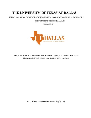
- 2. LAYOUTFOR CASCODESTAGEOF TWO NMOS IN LNA: PARASITIC RESISTANCECALCULATION: Rpoly= 7 ohm/sq, RM1 =0.0709 ohm/sq , RM2,3 =0.0639 ohm/sq Width of each NMOS = WNFET = 40um Number of fingers = NF = 40 Width of each finger = WF = 1um Length of each finger = LF = 0.12um Widths of gate around the contact : WPCONT = 0.2um, Wp = 0.4um Width of external gate between transistor and contact = Wext = 0.08um Lp = 18.84um Npcont = Lp/Wp = 47 Wcont = 0.16um Rgp = 1 𝑁 𝑓 [ 𝑊 𝑓𝑖𝑛𝑔𝑒𝑟 12∗𝐿 𝑅 𝑝𝑜𝑙𝑦 + 𝑊 𝑓𝑖𝑛𝑔𝑒𝑟 2∗𝐿 𝑅 𝑝𝑜𝑙𝑦 + ( 𝑊 𝑓𝑖𝑛𝑔𝑒𝑟 𝑊 𝑝 + 0.5) 𝑅 𝑝𝑜𝑙𝑦 2 ] Rgp = 1 40 [ 1𝑢𝑚 12∗0.13𝑢𝑚 7 + 0.08 2∗0.12𝑢𝑚 7 + ( 0.2 0.4 + 0.5) 7 2 ]
- 3. Rgp =0.2ohm Rg,cont = 𝑅 𝑐𝑜𝑛𝑡 𝑁 𝑐𝑜𝑛𝑡 = 8/47 = 0.19ohm Rg = Rgp + 𝑅 𝑔,𝑐𝑜𝑛𝑡 2 =0.2 + (0.19/2) =0.3ohm METAL_GATE RESISTANCES: Lm 1,1 = 21.06um, Lm 1,2 = 0.78um, Lm 1,3 = 0.4um, Lm1 = 0.4um, Lm 1,s = 0.4um R1 = Lm 1,1−2 Lm1 3𝐿𝑚1 . Rm1 = ((21.06-2(0.5))/(3*0.5))*0.0709 =0.948ohm R2 = Lm 1,2−2 Lm1 𝐿𝑚1 . Rm1 = ((1.38-0.5)/0.5)*0.0709=0.25ohm R3 = Lm 1,3 𝐿𝑚1 . Rm1 = (0.4/0.4)*0.0709=0.0709ohm Rc1 = Rc2 = 0.035ohm Rmetal, g =(1/2)[R1 +2R2 +Rc1+Rc2} + R3 =(1/2)[0.948+0.125*2+0.035+0.035] +0.0709 = 0.7ohm Rvia1 =Rvia2 = 0.9/60 = 0.015ohm RTOTAL = Rg,POLY +Rg,metal +Rvia1 +Rvia2 = 0.3+0.7+0.015+0.015 =0.998ohm The parasitic resistance is reducedtoabout 1ohm by using multi-fingeredlayout andincreasing the number of parallel connections. Lm1 R1 Rc1 Lm1,2 R2 Rc2 Lm1,s Lm1,3 R3 Lm1,1
- 4. PARASITIC CAPACITANCECALCULATION: W = 80 um; 𝜑 𝑏 = 0.7341 , 𝜑 𝑏𝑠𝑤 = 0.6662, 𝜑 𝑏𝑠𝑤𝑔 = 1.40 , Cj = 0.00105, Cjsw =1.1*10^(-10), Cjswg =3.5*10^(-10), Mj =0.3647, Mjsw = 1.052, Mjswg =0.732 Cgbo=17.06p; Cgdl=330p; Cgsl=330p; dlc=34.47n Cox=3.9*8.85*10E-12/3.12*E-9=0.011 Cgso=Cox*dlc-Cgsl=Cox*34.47*E-9-3.3*E-10= 5.13E-11 F/m Cgs=2/3CoxW*(L-2Lov)+Cgso*w=2/3*Cox*80E-6*(0.12E-6-2*1.4E-8)+ Cgso*80E-6 + NfCgb0L= 58f+4.104f+0.0818f=62.2fF Cgdo=Cox*dlc-Cgdl= Cox*34.47E-9-3.3E-10= Cgso = 5.13E-11 F/m Cgbo=2*dwc*Cox=3.76E-11F/m Cgd = CgdoW = -5.13E-11 x80E-6=4.104fF Cin = Cgs+2Cgd = 70.408fF Cdb=Area*Cjo*(1-Vbd/ φb) mj+Perimeter* Cjswo*(1-Vbd/ φbsw)mjsw Cdb=25*6E-6*0.36E-6*1E-4*(1+1.093/0.6)^0.5+(2*6+0.36*25)E-6*2E-10*(1+1.093/0.6)^0.5=63.44Ff ANALYSIS OF TUNING IN AN INPUT MATCHED LNA BYUSING Cgs IN COMMON STAGE OF LNA: Since in a cascaded LNA,CT = 1/(2wZoQin) = Cgs + (1+(gm1/gm2))Cgd .The resonant frequency can be increased or decreased by decreasing or adding the additional Cgs capacitor across the CS stage.However, we can also see that Qin increases or decreases as CT decreases or increases correspondingly. It also affects the linearity, which is being simulated and analyzed from IIP3 simulation shown below: (a): Given: Qin = 2; Vds1 = 0.3V To get Id = 2mA, W = (Id * L) / ( Un.Cox * Vds2 ) = ((2*10-3 )* (120*10-9 ) / ( 147.1*10-6 * 0.32 ) = 18um For input matching: Lg = (2 * Zo * Qin) / w = (2*50*2) / (2*3.14*2.4*(109)) = 13.269nH Ls = Zo / (gm*Qin*(2*Zo*w)) = Ls = (50)/(10*10-3*2*2*50*2*3.14*2.4*109) = 1.6587nH CT = 1/(w*(2*Zo)*Qin) = 1/(2*50*2*3.14*2.4*109 *2) = 0.33174pF Cin = Cgs+ 2Cgd = 16.66fF + (2*5.636) = 0.33174pF Additional Cgs = CT – Cin = 0.30474pF
- 5. SCHEMATIC: IIP3_SIMULATION: For Qin =2, IIP3 = -1.94dbm
- 6. (b) For Qin =1.5: Additional Cgs = CT – Cin = 0.4153pF For Qin =1.5, IIP3 = 0.39dbm For Qin =0.5: Additional Cgs = CT – Cin = 1.3pF For Qin =0.5, IIP3 = 13.59dbm
- 7. (c): IIP3(mW) vs Qin: We know that IIP3 =( 8*(Vgs – Vt))/(4*Qin 2 *Zo*3𝜽) which causes the IIP3 increases as Qin decreases. Hence, the circuit becomes more Linear as Qin decreases. S-PARAMETER CALCULATION:
- 8. INPUT IMPEDENCE OUTPUT IMPEDENCE PARALLEL RESISTANCE: PARALLEL CAPACITANCE: