SlideShare a Scribd company logo
1 of 11
Download to read offline
423FIXED-BIAS
CONFIGURATION
FIG. 7.1
Fixed-bias configuration.
The general relationships that can be applied to the dc analysis of all FET amplifiers are
IG Х 0 A (7.1)
and ID = IS (7.2)
For JFETs and depletion-type MOSFETs and MESFETs, Shockley’s equation is applied
to relate the input and output quantities:
ID = IDSSa1 -
VGS
VP
b
2
(7.3)
For enhancement-type MOSFETs and MESFETs, the following equation is applicable:
ID = k(VGS - VT)2
(7.4)
It is particularly important to realize that all of the equations above are for the field-
effect transistor only! They do not change with each network configuration so long as the
device is in the active region. The network simply defines the level of current and voltage
associated with the operating point through its own set of equations. In reality, the dc solu-
tion of BJT and FET networks is the solution of simultaneous equations established by the
device and the network. The solution can be determined using a mathematical or graphical
approach—a fact to be demonstrated by the first few networks to be analyzed. However, as
noted earlier, the graphical approach is the most popular for FET networks and is employed
in this book.
The first few sections of this chapter are limited to JFETs and the graphical approach
to analysis. The depletion-type MOSFET will then be examined with its increased range
of operating points, followed by the enhancement-type MOSFET. Finally, problems of a
design nature are investigated to fully test the concepts and procedures introduced in the
chapter.
7.2 FIXED-BIAS CONFIGURATION
●
The simplest of biasing arrangements for the n-channel JFET appears in Fig. 7.1. Referred
to as the fixed-bias configuration, it is one of the few FET configurations that can be
solved just as directly using either a mathematical or a graphical approach. Both methods
are included in this section to demonstrate the difference between the two methods and
also to establish the fact that the same solution can be obtained using either approach.
FET BIASING424
FIG. 7.2
Network for dc analysis.
ID (mA)
VGS
2
VPVP 0
4
IDSS
IDSS
FIG. 7.3
Plotting Shockley’s equation.
ID (mA)
VGSVP 0
IDSS
Device
Network
Q-point
(solution) IDQ
VGSQ
= –VGG
FIG. 7.4
Finding the solution for the fixed-bias
configuration.
InFig.7.4,thefixedlevelofVGS hasbeensuperimposedasaverticallineat VGS = -VGG.
At any point on the vertical line, the level of VGS is -VGG—the level of ID must simply be
determined on this vertical line. The point where the two curves intersect is the common
solution to the configuration—commonly referred to as the quiescent or operating point.
The subscript Q will be applied to the drain current and gate-to-source voltage to identify
their levels at the Q-point. Note in Fig. 7.4 that the quiescent level of ID is determined by
drawing a horizontal line from the Q-point to the vertical ID axis. It is important to realize
The configuration of Fig. 7.1 includes the ac levels Vi and Vo and the coupling capacitors
(C1 and C2). Recall that the coupling capacitors are “open circuits” for the dc analysis and
low impedances (essentially short circuits) for the ac analysis. The resistor RG is present
to ensure that Vi appears at the input to the FET amplifier for the ac analysis (Chapter 8).
For the dc analysis,
IG Х 0 A
and VRG
= IGRG = (0 A)RG = 0 V
The zero-volt drop across RG permits replacing RG by a short-circuit equivalent, as appear-
ing in the network of Fig. 7.2, specifically redrawn for the dc analysis.
The fact that the negative terminal of the battery is connected directly to the defined
positive potential of VGS clearly reveals that the polarity of VGS is directly opposite to that
of VGG. Applying Kirchhoff’s voltage law in the clockwise direction of the indicated loop
of Fig. 7.2 results in
-VGG - VGS = 0
and VGS = -VGG (7.5)
Since VGG is a fixed dc supply, the voltage VGS is fixed in magnitude, resulting in the des-
ignation “fixed-bias configuration.”
The resulting level of drain current ID is now controlled by Shockley’s equation:
ID = IDSSa1 -
VGS
VP
b
2
Since VGS is a fixed quantity for this configuration, its magnitude and sign can simply be
substituted into Shockley’s equation and the resulting level of ID calculated. This is one of
the few instances in which a mathematical solution to a FET configuration is quite direct.
A graphical analysis would require a plot of Shockley’s equation as shown in Fig. 7.3.
Recall that choosing VGS = VP>2 will result in a drain current of IDSS>4 when plotting
the equation. For the analysis of this chapter, the three points defined by IDSS, VP, and the
intersection just described will be sufficient for plotting the curve.
425FIXED-BIAS
CONFIGURATION
that once the network of Fig. 7.1 is constructed and operating, the dc levels of ID and VGS
that will be measured by the meters of Fig. 7.5 are the quiescent values defined by Fig. 7.4.
+
–
VGG
G
S
Voltmeter
Ammeter
RD
VDD
IDQ
VGSQ
FIG. 7.5
Measuring the quiescent values of ID and VGS.
The drain-to-source voltage of the output section can be determined by applying
Kirchhoff’s voltage law as follows:
+VDS + IDRD - VDD = 0
and VDS = VDD - IDRD (7.6)
Recall that single-subscript voltages refer to the voltage at a point with respect to ground.
For the configuration of Fig. 7.2,
VS = 0 V (7.7)
Using double-subscript notation, we have
VDS = VD - VS
or VD = VDS + VS = VDS + 0 V
and VD = VDS (7.8)
In addition, VGS = VG - VS
or VG = VGS + VS = VGS + 0 V
and VG = VGS (7.9)
The fact that VD = VDS and VG = VGS is fairly obvious from the fact that VS = 0 V,
but the derivations above were included to emphasize the relationship that exists between
double-subscript and single-subscript notation. Since the configuration requires two dc sup-
plies, its use is limited and will not be included in the forthcoming list of the most common
FET configurations.
FET BIASING426
2 V
1 M
D
S
G
kΩ2
16 V
VP
= 10 mAIDSS
= –8 V+
–
VGS
Ω
+
–
FIG. 7.6
Example 7.1.
EXAMPLE 7.1 Determine the following for the network of Fig. 7.6:
a. VGSQ
.
b. IDQ
.
c. VDS.
d. VD.
e. VG.
f. VS.
Solution:
Mathematical Approach
a. VGSQ
= -VGG = ؊2 V
b. IDQ
= IDSSa1 -
VGS
VP
b
2
= 10 mAa1 -
-2 V
-8 V
b
2
= 10 mA(1 - 0.25)2
= 10 mA(0.75)2
= 10 mA(0.5625)
= 5.625 mA
c. VDS = VDD - IDRD = 16 V - (5.625 mA)(2 k⍀)
= 16 V - 11.25 V = 4.75 V
d. VD = VDS = 4.75 V
e. VG = VGS = ؊2 V
f. VS = 0 V
Graphical Approach The resulting Shockley curve and the vertical line at VGS = -2 V
are provided in Fig. 7.7. It is certainly difficult to read beyond the second place without
ID (mA)
VGS
VP
0
IDSS
ID
Q
= 10 mA
1
2
3
4
5
6
7
8
9
13567
= –8 V
4
IDSS = 2.5 mA
= 5.6 mA
2
VP VGSQ
= –VGG
Q-point
4 2
= –4 V = –2 V
–––––––8–
FIG. 7.7
Graphical solution for the network of Fig. 7.6.
427SELF-BIAS
CONFIGURATION
significantly increasing the size of the figure, but a solution of 5.6 mA from the graph of
Fig. 7.7 is quite acceptable.
a. Therefore,
VGSQ
= -VGG = ؊2 V
b. IDQ
= 5.6 mA
c. VDS = VDD - IDRD = 16 V - (5.6 mA)(2 k⍀)
= 16 V - 11.2 V = 4.8 V
d. VD = VDS = 4.8 V
e. VG = VGS = ؊2 V
f. VS = 0 V
The results clearly confirm the fact that the mathematical and graphical approaches
generate solutions that are quite close.
7.3 SELF-BIAS CONFIGURATION
●
The self-bias configuration eliminates the need for two dc supplies. The controlling gate-
to-source voltage is now determined by the voltage across a resistor RS introduced in the
source leg of the configuration as shown in Fig. 7.8.
FIG. 7.8
JFET self-bias configuration.
FIG. 7.9
DC analysis of the self-bias
configuration.
For the dc analysis, the capacitors can again be replaced by “open circuits” and the resis-
tor RG replaced by a short-circuit equivalent since IG = 0 A. The result is the network of
Fig. 7.9 for the important dc analysis.
The current through RS is the source current IS, but IS = ID and
VRS
= IDRS
For the indicated closed loop of Fig. 7.9, we find that
-VGS - VRS
= 0
and VGS = -VRS
or VGS = -IDRS (7.10)
Note in this case that VGS is a function of the output current ID and not fixed in magnitude
as occurred for the fixed-bias configuration.
Equation (7.10) is defined by the network configuration, and Shockley’s equation relates
the input and output quantities of the device. Both equations relate the same two variables,
ID and VGS, permitting either a mathematical or a graphical solution.
431VOLTAGE-DIVIDER
BIASING
d. Eq. (7.12): VS = IDRS
= (2.6 mA)(1 k⍀)
= 2.6 V
e. Eq. (7.13): VG = 0 V
f. Eq. (7.14): VD = VDS + VS = 8.82 V + 2.6 V = 11.42 V
or VD = VDD - IDRD = 20 V - (2.6 mA)(3.3 k⍀) = 11.42 V
EXAMPLE 7.3 Find the quiescent point for the network of Fig. 7.12 if:
a. RS = 100 ⍀.
b. RS = 10 k⍀.
Solution: Both RS ϭ 100 ⍀ and RS ϭ 10 k⍀ are plotted on Fig. 7.16.
a. For RS ϭ 100 ⍀:
IDQ
Х 6.4 mA
and from Eq. (7.10),
VGSQ
Х ؊0.64 V
b. For RS = 10 k⍀
VGSQ
Х ؊4.6 V
and from Eq. (7.10),
IDQ
Х 0.46 mA
In particular, note how lower levels of RS bring the load line of the network closer to the
ID axis, whereas increasing levels of RS bring the load line closer to the VGS axis.
7.4 VOLTAGE-DIVIDER BIASING
●
The voltage-divider bias arrangement applied to BJT transistor amplifiers is also applied to
FET amplifiers as demonstrated by Fig. 7.17. The basic construction is exactly the same,
but the dc analysis of each is quite different. IG = 0 A for FET amplifiers, but the magni-
tude of IB for common-emitter BJT amplifiers can affect the dc levels of current and volt-
age in both the input and output circuits. Recall that IB provides the link between input and
output circuits for the BJT voltage-divider configuration, whereas VGS does the same for
the FET configuration.
ID (mA)
VGS0
1
2
3
4
5
6
7
8
1356 4 2 –––––– (V)
Q-point
IDQ
6.4 mA≅
VGS = –4 V, ID = 0.4 mA
RS = 10 kΩ
VGSQ
≅ 4.6– V
RS = 100 Ω
GSID = 4 mA,V = 0.4 V– Q-point
FIG. 7.16
Example 7.3.
FET BIASING432
G
D
S
FIG. 7.17
Voltage-divider bias arrangement.
RD
G
D
S
VDD
R1
R2
VG
VGS
VRS
IG ≅ 0 A
VDDVDD
R1
R2 VG
–+
ID
IS
+
RS
–
+
–
+
–
(a) (b)
FIG. 7.18
Redrawn network of Fig. 7.17 for dc analysis.
The network of Fig. 7.17 is redrawn as shown in Fig. 7.18 for the dc analysis. Note
that all the capacitors, including the bypass capacitor CS, have been replaced by an “open-
circuit” equivalent in Fig. 7.18b. In addition, the source VDD was separated into two
equivalent sources to permit a further separation of the input and output regions of the
network. Since IG = 0 A, Kirchhoff’s current law requires that IR1
= IR2
, and the series
equivalent circuit appearing to the left of the figure can be used to find the level of VG. The
voltage VG, equal to the voltage across R2, can be found using the voltage-divider rule and
Fig. 7.18a as follows:
VG =
R2VDD
R1 + R2
(7.15)
Applying Kirchhoff’s voltage law in the clockwise direction to the indicated loop of
Fig. 7.18 results in
VG - VGS - VRS
= 0
and VGS = VG - VRS
433VOLTAGE-DIVIDER
BIASING
IDQ
VGSQ
FIG. 7.19
Sketching the network equation for the voltage-divider configuration.
Substituting VRS
= ISRS = IDRS, we have
VGS = VG - IDRS (7.16)
The result is an equation that continues to include the same two variables appearing in
Shockley’s equation: VGS and ID. The quantities VG and RS are fixed by the network con-
struction. Equation (7.16) is still the equation for a straight line, but the origin is no longer
a point in the plotting of the line. The procedure for plotting Eq. (7.16) is not a difficult one
and will proceed as follows. Since any straight line requires two points to be defined, let us
first use the fact that anywhere on the horizontal axis of Fig. 7.19 the current ID = 0 mA. If
we therefore select ID to be 0 mA, we are in essence stating that we are somewhere on the
horizontal axis. The exact location can be determined simply by substituting ID = 0 mA
into Eq. (7.16) and finding the resulting value of VGS as follows:
VGS = VG - IDRS
= VG - (0 mA)RS
and VGS = VG 0 ID =0 mA (7.17)
The result specifies that whenever we plot Eq. (7.16), if we choose ID = 0 mA, the value
of VGS for the plot will be VG volts. The point just determined appears in Fig. 7.19.
Fortheotherpoint,letusnowemploythefactthatatanypointontheverticalaxisVGS = 0 V
and solve for the resulting value of ID:
VGS = VG - IDRS
0 V = VG - IDRS
and ID =
VG
RS
`
VGS =0 V
(7.18)
The result specifies that whenever we plot Eq. (7.16), if VGS = 0 V, the level of ID is
determined by Eq. (7.18). This intersection also appears on Fig. 7.19.
The two points defined above permit the drawing of a straight line to represent Eq. (7.16).
The intersection of the straight line with the transfer curve in the region to the left of the verti-
cal axis will define the operating point and the corresponding levels of ID and VGS.
Since the intersection on the vertical axis is determined by ID = VG>RS and VG is fixed
by the input network, increasing values of RS will reduce the level of the ID intersection as
FET BIASING434
FIG. 7.20
Effect of RS on the resulting Q-point.
G
D
S
R2
C1
C2
R1
RD
RS CS
FIG. 7.21
Example 7.4.
shown in Fig. 7.20. It is fairly obvious from Fig. 7.20 that:
Increasing values of RS result in lower quiescent values of ID and declining values
of VGS.
Once the quiescent values of IDQ
and VGSQ
are determined, the remaining network analy-
sis can be performed in the usual manner. That is,
VDS = VDD - ID(RD + RS) (7.19)
VD = VDD - IDRD (7.20)
VS = IDRS (7.21)
IR1
= IR2
=
VDD
R1 + R2
(7.22)
EXAMPLE 7.4 Determine the following for the network of Fig. 7.21:
a. IDQ
and VGSQ
.
b. VD.
c. VS.
d. VDS.
e. VDG.
435VOLTAGE-DIVIDER
BIASING
Solution:
a. For the transfer characteristics, if ID = IDSS>4 = 8 mA>4 = 2 mA, then VGS =
VP>2 = -4 V>2 = -2 V. The resulting curve representing Shockley’s equation
appears in Fig. 7.22. The network equation is defined by
VG =
R2VDD
R1 + R2
=
(270 k⍀)(16 V)
2.1 M⍀ + 0.27 M⍀
= 1.82 V
and VGS = VG - IDRS
= 1.82 V - ID(1.5 k⍀)
0
2
3
4
5
6
7
8
1–2–3–4–
Q-point
(I )DSS
ID (mA)
1 2 3
VP( ) VGS = –1.8 V 1.82 VVG =
ID( )
1
ID
Q
2.4 mA=
ID = 1.21 mA VGS( )= 0 V
= 0 mA
Q
FIG. 7.22
Determining the Q-point for the network of Fig. 7.21.
When ID = 0 mA,
VGS = +1.82 V
When VGS = 0 V,
ID =
1.82 V
1.5 k⍀
= 1.21 mA
The resulting bias line appears on Fig. 7.22 with quiescent values of
IDQ
= 2.4 mA
and VGSQ
= ؊1.8 V
b. VD = VDD - IDRD
= 16 V - (2.4 mA)(2.4 k⍀)
= 10.24 V
c. VS = IDRS = (2.4 mA)(1.5 k⍀)
= 3.6 V
d. VDS = VDD - ID(RD + RS)
= 16 V - (2.4 mA)(2.4 k⍀ + 1.5 k⍀)
= 6.64 V
or VDS = VD - VS = 10.24 V - 3.6 V
= 6.64 V
FET BIASING436 e. Although seldom requested, the voltage VDG can easily be determined using
VDG = VD - VG
= 10.24 V - 1.82 V
= 8.42 V
7.5 COMMON-GATE CONFIGURATION
●
The next configuration is one in which the gate terminal is grounded and the input signal
typically applied to the source terminal and the output signal obtained at the drain terminal
as shown in Fig. 7.23a. The network can also be drawn as shown in Fig. 7.23b.
FIG. 7.24
Determining the network
equation for the configuration of
Fig. 7.23.
RD
ID
DDV
oV
2C
1C
RS
VSS
(a)
VP
IDSS
iV
D
G
S
VP
VDD
IDSS
RD
oV
2C
iV
1C
(b)
–
+
RS
VSS
–
+
S D
G
FIG. 7.23
Two versions of the common-gate configuration.
The network equation can be determined using Fig. 7.24.
Applying Kirchhoff’s voltage law in the direction shown in Fig. 7.24 will result in
-VGS - ISRS + VSS = 0
and VGS = VSS - ISRS
but IS = ID
so VGS = VSS - IDRS (7.23)
Applying the condition ID = 0 mA to Eq. 7.23 will result in
VGS = VSS - (0)RS
and VGS = VSS 0 ID =0mA (7.24)
Applying the condition VGS = 0 V to Eq. 7.23 will result in
0 = VSS - IDRS
and ID =
VSS
RS
`
VGS =0 V
(7.25)
The resulting load-line appears in Fig. 7.25 intersecting the transfer curve for the JFET
as shown in the figure.
The resulting intersection defines the operating current IDQ
and voltage VDQ
for the net-
work as also indicated in the network.

More Related Content

What's hot (20)

Op-amp.pptx
Op-amp.pptxOp-amp.pptx
Op-amp.pptx
 
(Latest) topic 5 field_effect_transistors
(Latest) topic 5 field_effect_transistors(Latest) topic 5 field_effect_transistors
(Latest) topic 5 field_effect_transistors
 
Diodes basics
Diodes   basicsDiodes   basics
Diodes basics
 
Varactor theory
Varactor theoryVaractor theory
Varactor theory
 
Ota
OtaOta
Ota
 
Presentation on JFET
Presentation on JFETPresentation on JFET
Presentation on JFET
 
Operational Amplifier Design
Operational Amplifier DesignOperational Amplifier Design
Operational Amplifier Design
 
Semiconductor diode | semiconductor diode ppt | semiconductor diode for schoo...
Semiconductor diode | semiconductor diode ppt | semiconductor diode for schoo...Semiconductor diode | semiconductor diode ppt | semiconductor diode for schoo...
Semiconductor diode | semiconductor diode ppt | semiconductor diode for schoo...
 
MOSFET AND JFET
MOSFET AND JFETMOSFET AND JFET
MOSFET AND JFET
 
CMOS Fabrication using P-well -VLSI
CMOS Fabrication  using P-well -VLSICMOS Fabrication  using P-well -VLSI
CMOS Fabrication using P-well -VLSI
 
MOSFET as an Amplifier
MOSFET as an AmplifierMOSFET as an Amplifier
MOSFET as an Amplifier
 
Fabrication of diodes, resistors, capacitors, fe ts
Fabrication of diodes, resistors, capacitors, fe tsFabrication of diodes, resistors, capacitors, fe ts
Fabrication of diodes, resistors, capacitors, fe ts
 
Diode
DiodeDiode
Diode
 
FET (Field Effect Transistors)
FET (Field Effect Transistors)FET (Field Effect Transistors)
FET (Field Effect Transistors)
 
Band pass filter
Band pass filterBand pass filter
Band pass filter
 
Diode v i characteristic
Diode v i characteristicDiode v i characteristic
Diode v i characteristic
 
Clippers and clampers
Clippers and clampersClippers and clampers
Clippers and clampers
 
Differential amplifier
Differential amplifierDifferential amplifier
Differential amplifier
 
Mosfet
MosfetMosfet
Mosfet
 
Diode
DiodeDiode
Diode
 

Similar to Fet biasing boylestad pages

FET_Biasing.pdf
FET_Biasing.pdfFET_Biasing.pdf
FET_Biasing.pdfKarimB15
 
Analog Electronic Circuits - Module 2.2
Analog Electronic Circuits - Module 2.2Analog Electronic Circuits - Module 2.2
Analog Electronic Circuits - Module 2.2Aravinda Koithyar
 
2820.pdf
2820.pdf2820.pdf
2820.pdfGunaG14
 
GRID SIDE CONVERTER CONTROL IN DFIG BASED WIND SYSTEM USING ENHANCED HYSTERES...
GRID SIDE CONVERTER CONTROL IN DFIG BASED WIND SYSTEM USING ENHANCED HYSTERES...GRID SIDE CONVERTER CONTROL IN DFIG BASED WIND SYSTEM USING ENHANCED HYSTERES...
GRID SIDE CONVERTER CONTROL IN DFIG BASED WIND SYSTEM USING ENHANCED HYSTERES...ecij
 
note_1474205380.pdf
note_1474205380.pdfnote_1474205380.pdf
note_1474205380.pdfGunaG14
 
FET lecture_Electronics by Arif Sir
FET lecture_Electronics by Arif SirFET lecture_Electronics by Arif Sir
FET lecture_Electronics by Arif SirMuntasir Mahdi
 
RAZAVI - Design of Analog CMOS Integrated Circuits.pdf
RAZAVI - Design of Analog CMOS Integrated Circuits.pdfRAZAVI - Design of Analog CMOS Integrated Circuits.pdf
RAZAVI - Design of Analog CMOS Integrated Circuits.pdfivan ion
 
High Speed, Low Power Current Comparators with Hysteresis
High Speed, Low Power Current Comparators with HysteresisHigh Speed, Low Power Current Comparators with Hysteresis
High Speed, Low Power Current Comparators with HysteresisVLSICS Design
 
Interpret the diode equivalent circuit
Interpret the diode equivalent circuitInterpret the diode equivalent circuit
Interpret the diode equivalent circuitmanojmanoj218596
 
Common Source Characteristics - JFET
Common Source Characteristics - JFETCommon Source Characteristics - JFET
Common Source Characteristics - JFETDoCircuits
 
12 11jan17 24 oct16 13127 28779-1-ed(edit-new)
12 11jan17 24 oct16 13127 28779-1-ed(edit-new)12 11jan17 24 oct16 13127 28779-1-ed(edit-new)
12 11jan17 24 oct16 13127 28779-1-ed(edit-new)IAESIJEECS
 

Similar to Fet biasing boylestad pages (20)

FET_Biasing.pdf
FET_Biasing.pdfFET_Biasing.pdf
FET_Biasing.pdf
 
Analog Electronic Circuits - Module 2.2
Analog Electronic Circuits - Module 2.2Analog Electronic Circuits - Module 2.2
Analog Electronic Circuits - Module 2.2
 
2820.pdf
2820.pdf2820.pdf
2820.pdf
 
FET
FETFET
FET
 
GRID SIDE CONVERTER CONTROL IN DFIG BASED WIND SYSTEM USING ENHANCED HYSTERES...
GRID SIDE CONVERTER CONTROL IN DFIG BASED WIND SYSTEM USING ENHANCED HYSTERES...GRID SIDE CONVERTER CONTROL IN DFIG BASED WIND SYSTEM USING ENHANCED HYSTERES...
GRID SIDE CONVERTER CONTROL IN DFIG BASED WIND SYSTEM USING ENHANCED HYSTERES...
 
GRID SIDE CONVERTER CONTROL IN DFIG BASED WIND SYSTEM USING ENHANCED HYSTERES...
GRID SIDE CONVERTER CONTROL IN DFIG BASED WIND SYSTEM USING ENHANCED HYSTERES...GRID SIDE CONVERTER CONTROL IN DFIG BASED WIND SYSTEM USING ENHANCED HYSTERES...
GRID SIDE CONVERTER CONTROL IN DFIG BASED WIND SYSTEM USING ENHANCED HYSTERES...
 
Fet basics-1
Fet basics-1Fet basics-1
Fet basics-1
 
Ch06
Ch06Ch06
Ch06
 
note_1474205380.pdf
note_1474205380.pdfnote_1474205380.pdf
note_1474205380.pdf
 
FET-BIASING.pdf
FET-BIASING.pdfFET-BIASING.pdf
FET-BIASING.pdf
 
FET lecture_Electronics by Arif Sir
FET lecture_Electronics by Arif SirFET lecture_Electronics by Arif Sir
FET lecture_Electronics by Arif Sir
 
Fe ts mosfet
Fe ts mosfetFe ts mosfet
Fe ts mosfet
 
Mosfet baising
Mosfet baisingMosfet baising
Mosfet baising
 
RAZAVI - Design of Analog CMOS Integrated Circuits.pdf
RAZAVI - Design of Analog CMOS Integrated Circuits.pdfRAZAVI - Design of Analog CMOS Integrated Circuits.pdf
RAZAVI - Design of Analog CMOS Integrated Circuits.pdf
 
High Speed, Low Power Current Comparators with Hysteresis
High Speed, Low Power Current Comparators with HysteresisHigh Speed, Low Power Current Comparators with Hysteresis
High Speed, Low Power Current Comparators with Hysteresis
 
Interpret the diode equivalent circuit
Interpret the diode equivalent circuitInterpret the diode equivalent circuit
Interpret the diode equivalent circuit
 
Implementation of Coupled Inductor Based 7-level Inverter with Reduced Switches
Implementation of Coupled Inductor Based 7-level Inverter with Reduced SwitchesImplementation of Coupled Inductor Based 7-level Inverter with Reduced Switches
Implementation of Coupled Inductor Based 7-level Inverter with Reduced Switches
 
Common Source Characteristics - JFET
Common Source Characteristics - JFETCommon Source Characteristics - JFET
Common Source Characteristics - JFET
 
12 11jan17 24 oct16 13127 28779-1-ed(edit-new)
12 11jan17 24 oct16 13127 28779-1-ed(edit-new)12 11jan17 24 oct16 13127 28779-1-ed(edit-new)
12 11jan17 24 oct16 13127 28779-1-ed(edit-new)
 

More from LingalaSowjanya (20)

8251 communication interface
8251 communication interface8251 communication interface
8251 communication interface
 
ADDRESSING MODES OF 8085
ADDRESSING MODES OF 8085 ADDRESSING MODES OF 8085
ADDRESSING MODES OF 8085
 
(724429257) cylindrical coordinate system (1)
(724429257) cylindrical coordinate system (1)(724429257) cylindrical coordinate system (1)
(724429257) cylindrical coordinate system (1)
 
01analog filters
01analog filters01analog filters
01analog filters
 
Wave analysers
Wave analysersWave analysers
Wave analysers
 
Transducers (1)
Transducers (1)Transducers (1)
Transducers (1)
 
Thermocouple
ThermocoupleThermocouple
Thermocouple
 
Thermistor
ThermistorThermistor
Thermistor
 
Temperature measurement
Temperature measurementTemperature measurement
Temperature measurement
 
Strain gauge
Strain gaugeStrain gauge
Strain gauge
 
Rtd
RtdRtd
Rtd
 
Pressure measurement
Pressure measurementPressure measurement
Pressure measurement
 
Oscillators (1)
Oscillators (1)Oscillators (1)
Oscillators (1)
 
Multivibrators (1)
Multivibrators (1)Multivibrators (1)
Multivibrators (1)
 
Lvdt
LvdtLvdt
Lvdt
 
Classification of transducer
Classification of transducerClassification of transducer
Classification of transducer
 
Wheatstone bridge
Wheatstone bridgeWheatstone bridge
Wheatstone bridge
 
Energy meter
Energy meterEnergy meter
Energy meter
 
Bridges problems
Bridges   problemsBridges   problems
Bridges problems
 
Bridge ppt 1
Bridge ppt 1Bridge ppt 1
Bridge ppt 1
 

Recently uploaded

pipeline in computer architecture design
pipeline in computer architecture  designpipeline in computer architecture  design
pipeline in computer architecture designssuser87fa0c1
 
GDSC ASEB Gen AI study jams presentation
GDSC ASEB Gen AI study jams presentationGDSC ASEB Gen AI study jams presentation
GDSC ASEB Gen AI study jams presentationGDSCAESB
 
Arduino_CSE ece ppt for working and principal of arduino.ppt
Arduino_CSE ece ppt for working and principal of arduino.pptArduino_CSE ece ppt for working and principal of arduino.ppt
Arduino_CSE ece ppt for working and principal of arduino.pptSAURABHKUMAR892774
 
Internship report on mechanical engineering
Internship report on mechanical engineeringInternship report on mechanical engineering
Internship report on mechanical engineeringmalavadedarshan25
 
Software and Systems Engineering Standards: Verification and Validation of Sy...
Software and Systems Engineering Standards: Verification and Validation of Sy...Software and Systems Engineering Standards: Verification and Validation of Sy...
Software and Systems Engineering Standards: Verification and Validation of Sy...VICTOR MAESTRE RAMIREZ
 
IVE Industry Focused Event - Defence Sector 2024
IVE Industry Focused Event - Defence Sector 2024IVE Industry Focused Event - Defence Sector 2024
IVE Industry Focused Event - Defence Sector 2024Mark Billinghurst
 
Study on Air-Water & Water-Water Heat Exchange in a Finned Tube Exchanger
Study on Air-Water & Water-Water Heat Exchange in a Finned Tube ExchangerStudy on Air-Water & Water-Water Heat Exchange in a Finned Tube Exchanger
Study on Air-Water & Water-Water Heat Exchange in a Finned Tube ExchangerAnamika Sarkar
 
HARMONY IN THE NATURE AND EXISTENCE - Unit-IV
HARMONY IN THE NATURE AND EXISTENCE - Unit-IVHARMONY IN THE NATURE AND EXISTENCE - Unit-IV
HARMONY IN THE NATURE AND EXISTENCE - Unit-IVRajaP95
 
An experimental study in using natural admixture as an alternative for chemic...
An experimental study in using natural admixture as an alternative for chemic...An experimental study in using natural admixture as an alternative for chemic...
An experimental study in using natural admixture as an alternative for chemic...Chandu841456
 
Biology for Computer Engineers Course Handout.pptx
Biology for Computer Engineers Course Handout.pptxBiology for Computer Engineers Course Handout.pptx
Biology for Computer Engineers Course Handout.pptxDeepakSakkari2
 
CCS355 Neural Networks & Deep Learning Unit 1 PDF notes with Question bank .pdf
CCS355 Neural Networks & Deep Learning Unit 1 PDF notes with Question bank .pdfCCS355 Neural Networks & Deep Learning Unit 1 PDF notes with Question bank .pdf
CCS355 Neural Networks & Deep Learning Unit 1 PDF notes with Question bank .pdfAsst.prof M.Gokilavani
 
Past, Present and Future of Generative AI
Past, Present and Future of Generative AIPast, Present and Future of Generative AI
Past, Present and Future of Generative AIabhishek36461
 
Oxy acetylene welding presentation note.
Oxy acetylene welding presentation note.Oxy acetylene welding presentation note.
Oxy acetylene welding presentation note.eptoze12
 
CCS355 Neural Network & Deep Learning UNIT III notes and Question bank .pdf
CCS355 Neural Network & Deep Learning UNIT III notes and Question bank .pdfCCS355 Neural Network & Deep Learning UNIT III notes and Question bank .pdf
CCS355 Neural Network & Deep Learning UNIT III notes and Question bank .pdfAsst.prof M.Gokilavani
 
DATA ANALYTICS PPT definition usage example
DATA ANALYTICS PPT definition usage exampleDATA ANALYTICS PPT definition usage example
DATA ANALYTICS PPT definition usage examplePragyanshuParadkar1
 
Introduction-To-Agricultural-Surveillance-Rover.pptx
Introduction-To-Agricultural-Surveillance-Rover.pptxIntroduction-To-Agricultural-Surveillance-Rover.pptx
Introduction-To-Agricultural-Surveillance-Rover.pptxk795866
 
Risk Assessment For Installation of Drainage Pipes.pdf
Risk Assessment For Installation of Drainage Pipes.pdfRisk Assessment For Installation of Drainage Pipes.pdf
Risk Assessment For Installation of Drainage Pipes.pdfROCENODodongVILLACER
 
INFLUENCE OF NANOSILICA ON THE PROPERTIES OF CONCRETE
INFLUENCE OF NANOSILICA ON THE PROPERTIES OF CONCRETEINFLUENCE OF NANOSILICA ON THE PROPERTIES OF CONCRETE
INFLUENCE OF NANOSILICA ON THE PROPERTIES OF CONCRETEroselinkalist12
 
Call Us ≽ 8377877756 ≼ Call Girls In Shastri Nagar (Delhi)
Call Us ≽ 8377877756 ≼ Call Girls In Shastri Nagar (Delhi)Call Us ≽ 8377877756 ≼ Call Girls In Shastri Nagar (Delhi)
Call Us ≽ 8377877756 ≼ Call Girls In Shastri Nagar (Delhi)dollysharma2066
 
What are the advantages and disadvantages of membrane structures.pptx
What are the advantages and disadvantages of membrane structures.pptxWhat are the advantages and disadvantages of membrane structures.pptx
What are the advantages and disadvantages of membrane structures.pptxwendy cai
 

Recently uploaded (20)

pipeline in computer architecture design
pipeline in computer architecture  designpipeline in computer architecture  design
pipeline in computer architecture design
 
GDSC ASEB Gen AI study jams presentation
GDSC ASEB Gen AI study jams presentationGDSC ASEB Gen AI study jams presentation
GDSC ASEB Gen AI study jams presentation
 
Arduino_CSE ece ppt for working and principal of arduino.ppt
Arduino_CSE ece ppt for working and principal of arduino.pptArduino_CSE ece ppt for working and principal of arduino.ppt
Arduino_CSE ece ppt for working and principal of arduino.ppt
 
Internship report on mechanical engineering
Internship report on mechanical engineeringInternship report on mechanical engineering
Internship report on mechanical engineering
 
Software and Systems Engineering Standards: Verification and Validation of Sy...
Software and Systems Engineering Standards: Verification and Validation of Sy...Software and Systems Engineering Standards: Verification and Validation of Sy...
Software and Systems Engineering Standards: Verification and Validation of Sy...
 
IVE Industry Focused Event - Defence Sector 2024
IVE Industry Focused Event - Defence Sector 2024IVE Industry Focused Event - Defence Sector 2024
IVE Industry Focused Event - Defence Sector 2024
 
Study on Air-Water & Water-Water Heat Exchange in a Finned Tube Exchanger
Study on Air-Water & Water-Water Heat Exchange in a Finned Tube ExchangerStudy on Air-Water & Water-Water Heat Exchange in a Finned Tube Exchanger
Study on Air-Water & Water-Water Heat Exchange in a Finned Tube Exchanger
 
HARMONY IN THE NATURE AND EXISTENCE - Unit-IV
HARMONY IN THE NATURE AND EXISTENCE - Unit-IVHARMONY IN THE NATURE AND EXISTENCE - Unit-IV
HARMONY IN THE NATURE AND EXISTENCE - Unit-IV
 
An experimental study in using natural admixture as an alternative for chemic...
An experimental study in using natural admixture as an alternative for chemic...An experimental study in using natural admixture as an alternative for chemic...
An experimental study in using natural admixture as an alternative for chemic...
 
Biology for Computer Engineers Course Handout.pptx
Biology for Computer Engineers Course Handout.pptxBiology for Computer Engineers Course Handout.pptx
Biology for Computer Engineers Course Handout.pptx
 
CCS355 Neural Networks & Deep Learning Unit 1 PDF notes with Question bank .pdf
CCS355 Neural Networks & Deep Learning Unit 1 PDF notes with Question bank .pdfCCS355 Neural Networks & Deep Learning Unit 1 PDF notes with Question bank .pdf
CCS355 Neural Networks & Deep Learning Unit 1 PDF notes with Question bank .pdf
 
Past, Present and Future of Generative AI
Past, Present and Future of Generative AIPast, Present and Future of Generative AI
Past, Present and Future of Generative AI
 
Oxy acetylene welding presentation note.
Oxy acetylene welding presentation note.Oxy acetylene welding presentation note.
Oxy acetylene welding presentation note.
 
CCS355 Neural Network & Deep Learning UNIT III notes and Question bank .pdf
CCS355 Neural Network & Deep Learning UNIT III notes and Question bank .pdfCCS355 Neural Network & Deep Learning UNIT III notes and Question bank .pdf
CCS355 Neural Network & Deep Learning UNIT III notes and Question bank .pdf
 
DATA ANALYTICS PPT definition usage example
DATA ANALYTICS PPT definition usage exampleDATA ANALYTICS PPT definition usage example
DATA ANALYTICS PPT definition usage example
 
Introduction-To-Agricultural-Surveillance-Rover.pptx
Introduction-To-Agricultural-Surveillance-Rover.pptxIntroduction-To-Agricultural-Surveillance-Rover.pptx
Introduction-To-Agricultural-Surveillance-Rover.pptx
 
Risk Assessment For Installation of Drainage Pipes.pdf
Risk Assessment For Installation of Drainage Pipes.pdfRisk Assessment For Installation of Drainage Pipes.pdf
Risk Assessment For Installation of Drainage Pipes.pdf
 
INFLUENCE OF NANOSILICA ON THE PROPERTIES OF CONCRETE
INFLUENCE OF NANOSILICA ON THE PROPERTIES OF CONCRETEINFLUENCE OF NANOSILICA ON THE PROPERTIES OF CONCRETE
INFLUENCE OF NANOSILICA ON THE PROPERTIES OF CONCRETE
 
Call Us ≽ 8377877756 ≼ Call Girls In Shastri Nagar (Delhi)
Call Us ≽ 8377877756 ≼ Call Girls In Shastri Nagar (Delhi)Call Us ≽ 8377877756 ≼ Call Girls In Shastri Nagar (Delhi)
Call Us ≽ 8377877756 ≼ Call Girls In Shastri Nagar (Delhi)
 
What are the advantages and disadvantages of membrane structures.pptx
What are the advantages and disadvantages of membrane structures.pptxWhat are the advantages and disadvantages of membrane structures.pptx
What are the advantages and disadvantages of membrane structures.pptx
 

Fet biasing boylestad pages

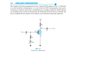
  • 1. 423FIXED-BIAS CONFIGURATION FIG. 7.1 Fixed-bias configuration. The general relationships that can be applied to the dc analysis of all FET amplifiers are IG Х 0 A (7.1) and ID = IS (7.2) For JFETs and depletion-type MOSFETs and MESFETs, Shockley’s equation is applied to relate the input and output quantities: ID = IDSSa1 - VGS VP b 2 (7.3) For enhancement-type MOSFETs and MESFETs, the following equation is applicable: ID = k(VGS - VT)2 (7.4) It is particularly important to realize that all of the equations above are for the field- effect transistor only! They do not change with each network configuration so long as the device is in the active region. The network simply defines the level of current and voltage associated with the operating point through its own set of equations. In reality, the dc solu- tion of BJT and FET networks is the solution of simultaneous equations established by the device and the network. The solution can be determined using a mathematical or graphical approach—a fact to be demonstrated by the first few networks to be analyzed. However, as noted earlier, the graphical approach is the most popular for FET networks and is employed in this book. The first few sections of this chapter are limited to JFETs and the graphical approach to analysis. The depletion-type MOSFET will then be examined with its increased range of operating points, followed by the enhancement-type MOSFET. Finally, problems of a design nature are investigated to fully test the concepts and procedures introduced in the chapter. 7.2 FIXED-BIAS CONFIGURATION ● The simplest of biasing arrangements for the n-channel JFET appears in Fig. 7.1. Referred to as the fixed-bias configuration, it is one of the few FET configurations that can be solved just as directly using either a mathematical or a graphical approach. Both methods are included in this section to demonstrate the difference between the two methods and also to establish the fact that the same solution can be obtained using either approach.
  • 2. FET BIASING424 FIG. 7.2 Network for dc analysis. ID (mA) VGS 2 VPVP 0 4 IDSS IDSS FIG. 7.3 Plotting Shockley’s equation. ID (mA) VGSVP 0 IDSS Device Network Q-point (solution) IDQ VGSQ = –VGG FIG. 7.4 Finding the solution for the fixed-bias configuration. InFig.7.4,thefixedlevelofVGS hasbeensuperimposedasaverticallineat VGS = -VGG. At any point on the vertical line, the level of VGS is -VGG—the level of ID must simply be determined on this vertical line. The point where the two curves intersect is the common solution to the configuration—commonly referred to as the quiescent or operating point. The subscript Q will be applied to the drain current and gate-to-source voltage to identify their levels at the Q-point. Note in Fig. 7.4 that the quiescent level of ID is determined by drawing a horizontal line from the Q-point to the vertical ID axis. It is important to realize The configuration of Fig. 7.1 includes the ac levels Vi and Vo and the coupling capacitors (C1 and C2). Recall that the coupling capacitors are “open circuits” for the dc analysis and low impedances (essentially short circuits) for the ac analysis. The resistor RG is present to ensure that Vi appears at the input to the FET amplifier for the ac analysis (Chapter 8). For the dc analysis, IG Х 0 A and VRG = IGRG = (0 A)RG = 0 V The zero-volt drop across RG permits replacing RG by a short-circuit equivalent, as appear- ing in the network of Fig. 7.2, specifically redrawn for the dc analysis. The fact that the negative terminal of the battery is connected directly to the defined positive potential of VGS clearly reveals that the polarity of VGS is directly opposite to that of VGG. Applying Kirchhoff’s voltage law in the clockwise direction of the indicated loop of Fig. 7.2 results in -VGG - VGS = 0 and VGS = -VGG (7.5) Since VGG is a fixed dc supply, the voltage VGS is fixed in magnitude, resulting in the des- ignation “fixed-bias configuration.” The resulting level of drain current ID is now controlled by Shockley’s equation: ID = IDSSa1 - VGS VP b 2 Since VGS is a fixed quantity for this configuration, its magnitude and sign can simply be substituted into Shockley’s equation and the resulting level of ID calculated. This is one of the few instances in which a mathematical solution to a FET configuration is quite direct. A graphical analysis would require a plot of Shockley’s equation as shown in Fig. 7.3. Recall that choosing VGS = VP>2 will result in a drain current of IDSS>4 when plotting the equation. For the analysis of this chapter, the three points defined by IDSS, VP, and the intersection just described will be sufficient for plotting the curve.
  • 3. 425FIXED-BIAS CONFIGURATION that once the network of Fig. 7.1 is constructed and operating, the dc levels of ID and VGS that will be measured by the meters of Fig. 7.5 are the quiescent values defined by Fig. 7.4. + – VGG G S Voltmeter Ammeter RD VDD IDQ VGSQ FIG. 7.5 Measuring the quiescent values of ID and VGS. The drain-to-source voltage of the output section can be determined by applying Kirchhoff’s voltage law as follows: +VDS + IDRD - VDD = 0 and VDS = VDD - IDRD (7.6) Recall that single-subscript voltages refer to the voltage at a point with respect to ground. For the configuration of Fig. 7.2, VS = 0 V (7.7) Using double-subscript notation, we have VDS = VD - VS or VD = VDS + VS = VDS + 0 V and VD = VDS (7.8) In addition, VGS = VG - VS or VG = VGS + VS = VGS + 0 V and VG = VGS (7.9) The fact that VD = VDS and VG = VGS is fairly obvious from the fact that VS = 0 V, but the derivations above were included to emphasize the relationship that exists between double-subscript and single-subscript notation. Since the configuration requires two dc sup- plies, its use is limited and will not be included in the forthcoming list of the most common FET configurations.
  • 4. FET BIASING426 2 V 1 M D S G kΩ2 16 V VP = 10 mAIDSS = –8 V+ – VGS Ω + – FIG. 7.6 Example 7.1. EXAMPLE 7.1 Determine the following for the network of Fig. 7.6: a. VGSQ . b. IDQ . c. VDS. d. VD. e. VG. f. VS. Solution: Mathematical Approach a. VGSQ = -VGG = ؊2 V b. IDQ = IDSSa1 - VGS VP b 2 = 10 mAa1 - -2 V -8 V b 2 = 10 mA(1 - 0.25)2 = 10 mA(0.75)2 = 10 mA(0.5625) = 5.625 mA c. VDS = VDD - IDRD = 16 V - (5.625 mA)(2 k⍀) = 16 V - 11.25 V = 4.75 V d. VD = VDS = 4.75 V e. VG = VGS = ؊2 V f. VS = 0 V Graphical Approach The resulting Shockley curve and the vertical line at VGS = -2 V are provided in Fig. 7.7. It is certainly difficult to read beyond the second place without ID (mA) VGS VP 0 IDSS ID Q = 10 mA 1 2 3 4 5 6 7 8 9 13567 = –8 V 4 IDSS = 2.5 mA = 5.6 mA 2 VP VGSQ = –VGG Q-point 4 2 = –4 V = –2 V –––––––8– FIG. 7.7 Graphical solution for the network of Fig. 7.6.
  • 5. 427SELF-BIAS CONFIGURATION significantly increasing the size of the figure, but a solution of 5.6 mA from the graph of Fig. 7.7 is quite acceptable. a. Therefore, VGSQ = -VGG = ؊2 V b. IDQ = 5.6 mA c. VDS = VDD - IDRD = 16 V - (5.6 mA)(2 k⍀) = 16 V - 11.2 V = 4.8 V d. VD = VDS = 4.8 V e. VG = VGS = ؊2 V f. VS = 0 V The results clearly confirm the fact that the mathematical and graphical approaches generate solutions that are quite close. 7.3 SELF-BIAS CONFIGURATION ● The self-bias configuration eliminates the need for two dc supplies. The controlling gate- to-source voltage is now determined by the voltage across a resistor RS introduced in the source leg of the configuration as shown in Fig. 7.8. FIG. 7.8 JFET self-bias configuration. FIG. 7.9 DC analysis of the self-bias configuration. For the dc analysis, the capacitors can again be replaced by “open circuits” and the resis- tor RG replaced by a short-circuit equivalent since IG = 0 A. The result is the network of Fig. 7.9 for the important dc analysis. The current through RS is the source current IS, but IS = ID and VRS = IDRS For the indicated closed loop of Fig. 7.9, we find that -VGS - VRS = 0 and VGS = -VRS or VGS = -IDRS (7.10) Note in this case that VGS is a function of the output current ID and not fixed in magnitude as occurred for the fixed-bias configuration. Equation (7.10) is defined by the network configuration, and Shockley’s equation relates the input and output quantities of the device. Both equations relate the same two variables, ID and VGS, permitting either a mathematical or a graphical solution.
  • 6. 431VOLTAGE-DIVIDER BIASING d. Eq. (7.12): VS = IDRS = (2.6 mA)(1 k⍀) = 2.6 V e. Eq. (7.13): VG = 0 V f. Eq. (7.14): VD = VDS + VS = 8.82 V + 2.6 V = 11.42 V or VD = VDD - IDRD = 20 V - (2.6 mA)(3.3 k⍀) = 11.42 V EXAMPLE 7.3 Find the quiescent point for the network of Fig. 7.12 if: a. RS = 100 ⍀. b. RS = 10 k⍀. Solution: Both RS ϭ 100 ⍀ and RS ϭ 10 k⍀ are plotted on Fig. 7.16. a. For RS ϭ 100 ⍀: IDQ Х 6.4 mA and from Eq. (7.10), VGSQ Х ؊0.64 V b. For RS = 10 k⍀ VGSQ Х ؊4.6 V and from Eq. (7.10), IDQ Х 0.46 mA In particular, note how lower levels of RS bring the load line of the network closer to the ID axis, whereas increasing levels of RS bring the load line closer to the VGS axis. 7.4 VOLTAGE-DIVIDER BIASING ● The voltage-divider bias arrangement applied to BJT transistor amplifiers is also applied to FET amplifiers as demonstrated by Fig. 7.17. The basic construction is exactly the same, but the dc analysis of each is quite different. IG = 0 A for FET amplifiers, but the magni- tude of IB for common-emitter BJT amplifiers can affect the dc levels of current and volt- age in both the input and output circuits. Recall that IB provides the link between input and output circuits for the BJT voltage-divider configuration, whereas VGS does the same for the FET configuration. ID (mA) VGS0 1 2 3 4 5 6 7 8 1356 4 2 –––––– (V) Q-point IDQ 6.4 mA≅ VGS = –4 V, ID = 0.4 mA RS = 10 kΩ VGSQ ≅ 4.6– V RS = 100 Ω GSID = 4 mA,V = 0.4 V– Q-point FIG. 7.16 Example 7.3.
  • 7. FET BIASING432 G D S FIG. 7.17 Voltage-divider bias arrangement. RD G D S VDD R1 R2 VG VGS VRS IG ≅ 0 A VDDVDD R1 R2 VG –+ ID IS + RS – + – + – (a) (b) FIG. 7.18 Redrawn network of Fig. 7.17 for dc analysis. The network of Fig. 7.17 is redrawn as shown in Fig. 7.18 for the dc analysis. Note that all the capacitors, including the bypass capacitor CS, have been replaced by an “open- circuit” equivalent in Fig. 7.18b. In addition, the source VDD was separated into two equivalent sources to permit a further separation of the input and output regions of the network. Since IG = 0 A, Kirchhoff’s current law requires that IR1 = IR2 , and the series equivalent circuit appearing to the left of the figure can be used to find the level of VG. The voltage VG, equal to the voltage across R2, can be found using the voltage-divider rule and Fig. 7.18a as follows: VG = R2VDD R1 + R2 (7.15) Applying Kirchhoff’s voltage law in the clockwise direction to the indicated loop of Fig. 7.18 results in VG - VGS - VRS = 0 and VGS = VG - VRS
  • 8. 433VOLTAGE-DIVIDER BIASING IDQ VGSQ FIG. 7.19 Sketching the network equation for the voltage-divider configuration. Substituting VRS = ISRS = IDRS, we have VGS = VG - IDRS (7.16) The result is an equation that continues to include the same two variables appearing in Shockley’s equation: VGS and ID. The quantities VG and RS are fixed by the network con- struction. Equation (7.16) is still the equation for a straight line, but the origin is no longer a point in the plotting of the line. The procedure for plotting Eq. (7.16) is not a difficult one and will proceed as follows. Since any straight line requires two points to be defined, let us first use the fact that anywhere on the horizontal axis of Fig. 7.19 the current ID = 0 mA. If we therefore select ID to be 0 mA, we are in essence stating that we are somewhere on the horizontal axis. The exact location can be determined simply by substituting ID = 0 mA into Eq. (7.16) and finding the resulting value of VGS as follows: VGS = VG - IDRS = VG - (0 mA)RS and VGS = VG 0 ID =0 mA (7.17) The result specifies that whenever we plot Eq. (7.16), if we choose ID = 0 mA, the value of VGS for the plot will be VG volts. The point just determined appears in Fig. 7.19. Fortheotherpoint,letusnowemploythefactthatatanypointontheverticalaxisVGS = 0 V and solve for the resulting value of ID: VGS = VG - IDRS 0 V = VG - IDRS and ID = VG RS ` VGS =0 V (7.18) The result specifies that whenever we plot Eq. (7.16), if VGS = 0 V, the level of ID is determined by Eq. (7.18). This intersection also appears on Fig. 7.19. The two points defined above permit the drawing of a straight line to represent Eq. (7.16). The intersection of the straight line with the transfer curve in the region to the left of the verti- cal axis will define the operating point and the corresponding levels of ID and VGS. Since the intersection on the vertical axis is determined by ID = VG>RS and VG is fixed by the input network, increasing values of RS will reduce the level of the ID intersection as
  • 9. FET BIASING434 FIG. 7.20 Effect of RS on the resulting Q-point. G D S R2 C1 C2 R1 RD RS CS FIG. 7.21 Example 7.4. shown in Fig. 7.20. It is fairly obvious from Fig. 7.20 that: Increasing values of RS result in lower quiescent values of ID and declining values of VGS. Once the quiescent values of IDQ and VGSQ are determined, the remaining network analy- sis can be performed in the usual manner. That is, VDS = VDD - ID(RD + RS) (7.19) VD = VDD - IDRD (7.20) VS = IDRS (7.21) IR1 = IR2 = VDD R1 + R2 (7.22) EXAMPLE 7.4 Determine the following for the network of Fig. 7.21: a. IDQ and VGSQ . b. VD. c. VS. d. VDS. e. VDG.
  • 10. 435VOLTAGE-DIVIDER BIASING Solution: a. For the transfer characteristics, if ID = IDSS>4 = 8 mA>4 = 2 mA, then VGS = VP>2 = -4 V>2 = -2 V. The resulting curve representing Shockley’s equation appears in Fig. 7.22. The network equation is defined by VG = R2VDD R1 + R2 = (270 k⍀)(16 V) 2.1 M⍀ + 0.27 M⍀ = 1.82 V and VGS = VG - IDRS = 1.82 V - ID(1.5 k⍀) 0 2 3 4 5 6 7 8 1–2–3–4– Q-point (I )DSS ID (mA) 1 2 3 VP( ) VGS = –1.8 V 1.82 VVG = ID( ) 1 ID Q 2.4 mA= ID = 1.21 mA VGS( )= 0 V = 0 mA Q FIG. 7.22 Determining the Q-point for the network of Fig. 7.21. When ID = 0 mA, VGS = +1.82 V When VGS = 0 V, ID = 1.82 V 1.5 k⍀ = 1.21 mA The resulting bias line appears on Fig. 7.22 with quiescent values of IDQ = 2.4 mA and VGSQ = ؊1.8 V b. VD = VDD - IDRD = 16 V - (2.4 mA)(2.4 k⍀) = 10.24 V c. VS = IDRS = (2.4 mA)(1.5 k⍀) = 3.6 V d. VDS = VDD - ID(RD + RS) = 16 V - (2.4 mA)(2.4 k⍀ + 1.5 k⍀) = 6.64 V or VDS = VD - VS = 10.24 V - 3.6 V = 6.64 V
  • 11. FET BIASING436 e. Although seldom requested, the voltage VDG can easily be determined using VDG = VD - VG = 10.24 V - 1.82 V = 8.42 V 7.5 COMMON-GATE CONFIGURATION ● The next configuration is one in which the gate terminal is grounded and the input signal typically applied to the source terminal and the output signal obtained at the drain terminal as shown in Fig. 7.23a. The network can also be drawn as shown in Fig. 7.23b. FIG. 7.24 Determining the network equation for the configuration of Fig. 7.23. RD ID DDV oV 2C 1C RS VSS (a) VP IDSS iV D G S VP VDD IDSS RD oV 2C iV 1C (b) – + RS VSS – + S D G FIG. 7.23 Two versions of the common-gate configuration. The network equation can be determined using Fig. 7.24. Applying Kirchhoff’s voltage law in the direction shown in Fig. 7.24 will result in -VGS - ISRS + VSS = 0 and VGS = VSS - ISRS but IS = ID so VGS = VSS - IDRS (7.23) Applying the condition ID = 0 mA to Eq. 7.23 will result in VGS = VSS - (0)RS and VGS = VSS 0 ID =0mA (7.24) Applying the condition VGS = 0 V to Eq. 7.23 will result in 0 = VSS - IDRS and ID = VSS RS ` VGS =0 V (7.25) The resulting load-line appears in Fig. 7.25 intersecting the transfer curve for the JFET as shown in the figure. The resulting intersection defines the operating current IDQ and voltage VDQ for the net- work as also indicated in the network.