SPICE MODEL of SSM3K15FV (Standard+BDS Model) in SPICE PARK
•
1 like•182 views

SPICE MODEL of SSM3K15FV (Standard+BDS) in SPICE PARK. English Version is http://www.spicepark.net. Japanese Version is http://www.spicepark.com by Bee Technologies.

Recommended
Recommended
More Related Content
What's hot
What's hot (20)
Similar to SPICE MODEL of SSM3K15FV (Standard+BDS Model) in SPICE PARK
Similar to SPICE MODEL of SSM3K15FV (Standard+BDS Model) in SPICE PARK (16)
More from Tsuyoshi Horigome
More from Tsuyoshi Horigome (20)
Recently uploaded
Recently uploaded (20)
SPICE MODEL of SSM3K15FV (Standard+BDS Model) in SPICE PARK
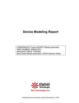
- 1. Device Modeling Report COMPONENTS: Power MOSFET (Model parameter) PART NUMBER: SSM3K15FV MANUFACTURER: TOSHIBA Body Diode (Model parameter) / ESD Protection Diode Bee Technologies Inc. All Rights Reserved Copyright (c) Bee Technologies Inc. 2007
- 2. Circuit Configuration U1 SSM3K15FV All Rights Reserved Copyright (c) Bee Technologies Inc. 2007
- 3. MOSFET MODEL PSpice model Model description parameter LEVEL L Channel Length W Channel Width KP Transconductance RS Source Ohmic Resistance RD Ohmic Drain Resistance VTO Zero-bias Threshold Voltage RDS Drain-Source Shunt Resistance TOX Gate Oxide Thickness CGSO Zero-bias Gate-Source Capacitance CGDO Zero-bias Gate-Drain Capacitance CBD Zero-bias Bulk-Drain Junction Capacitance MJ Bulk Junction Grading Coefficient PB Bulk Junction Potential FC Bulk Junction Forward-bias Capacitance Coefficient RG Gate Ohmic Resistance IS Bulk Junction Saturation Current N Bulk Junction Emission Coefficient RB Bulk Series Resistance PHI Surface Inversion Potential GAMMA Body-effect Parameter DELTA Width effect on Threshold Voltage ETA Static Feedback on Threshold Voltage THETA Mobility Modulation KAPPA Saturation Field Factor VMAX Maximum Drift Velocity of Carriers XJ Metallurgical Junction Depth UO Surface Mobility All Rights Reserved Copyright (c) Bee Technologies Inc. 2007
- 4. Transconductance Characteristic Circuit Simulation Result Comparison table gfs Id(mA) Error (%) Measurement Simulation 1 0.0200 0.020 0 2 0.0286 0.028 -2.098 5 0.0455 0.045 -1.099 10 0.0625 0.063 0.800 20 0.0870 0.089 2.299 50 0.1429 0.141 -1.330 100 0.2000 0.199 -0.500 All Rights Reserved Copyright (c) Bee Technologies Inc. 2007
- 5. Vgs-Id Characteristic Circuit Simulation result 1.0A 100mA 10mA 1.0mA 0V 1.0V 2.0V 3.0V 4.0V I(V3) V_V1 Evaluation circuit V3 0Vdc U1 V2 SSM3K15FV 3 V1 3 0 All Rights Reserved Copyright (c) Bee Technologies Inc. 2007
- 6. Comparison Graph Circuit Simulation Result Simulation Result VGS(V) ID(mA) Error (%) Measurement Simulation 1 1.43 1.4831 3.713 2 1.5 1.5256 1.707 5 1.62 1.6100 -0.617 10 1.72 1.7051 -0.866 20 1.88 1.8397 -2.144 50 2.15 2.1068 -2.009 100 2.45 2.4081 -1.710 All Rights Reserved Copyright (c) Bee Technologies Inc. 2007
- 7. Rds(on) Characteristic Circuit Simulation result 10mA 5mA 0A 0V 10mV 20mV 30mV 40mV 50mV I(V2) V_V3 Evaluation circuit V2 0Vdc U1 V3 0Vdc SSM3K15FV V1 4 0 Simulation Result ID=10mA, VGS=4V Measurement Simulation Error (%) R DS (on) 2.2 2.2243 1.105 All Rights Reserved Copyright (c) Bee Technologies Inc. 2007
- 8. Gate Charge Characteristic Circuit Simulation result 10V 8V 6V 4V 2V 0V 0s 0.2ns 0.4ns 0.6ns 0.8ns 1.0ns V(W1:3) Time*1m Evaluation circuit RON = 1 U1 ROFF = 1e9 ION = 0 IOFF = 10u W1 + I2 SSM3K15FV D1 - Dbreak W 0.091 I1 = 0 I1 I2 = 1m TD = 0 V1 TR = 10n TF = 10n PW = 200u PER = 500u 20 0 Simulation Result VDD=20V,ID=0.091A Measurement Simulation Error (%) Qgs (nC) 0.12 0.12 0 Qgd (nC) 0.28 0.28 0 Qg (nC) 1.136 0.862 -24.120 All Rights Reserved Copyright (c) Bee Technologies Inc. 2007
- 9. Gate Charge Characteristic Reference 10 VDD=20V 8 GATE VOLTAGE Vg 6 4 2 0 0 0.4 0.8 1.2 GATE CHARGE Qg(nc) All Rights Reserved Copyright (c) Bee Technologies Inc. 2007
- 10. Capacitance Characteristic Measurement Simulation Simulation Result Cbd(pF) VDS(V) Error(%) Measurement Simulation 0.1 10 10 0 0.2 9.5 9.52 0.211 0.5 8.5 8.5 0.000 1 7.5 7.44 -0.800 2 6.3 6.22 -1.270 5 4.7 4.71 0.213 10 3.7 3.73 0.811 20 2.9 2.92 0.690 30 2.6 2.53 -2.692 All Rights Reserved Copyright (c) Bee Technologies Inc. 2007
- 11. Switching Time Characteristic Circuit Simulation result 10V 5V 0V 1.5us 2.0us 2.5us 3.0us V(U1:G) V(U1:D) Time Evaluation circuit L1 R2 50nH 500 U1 R3 L2 V1 50 V1 = 0 V2 30nH V2 = 10 5 SSM3K15FV TD = 2u R4 TR = 4.5n TF = 4.5n 50 PW = 10u PER = 30u 0 Simulation Result ID=10m A, VDD=5V Measurement Simulation Error(%) VGS=0/5V Ton (ns) 50 49.848 -0.304 All Rights Reserved Copyright (c) Bee Technologies Inc. 2007
- 12. Output Characteristic Circuit Simulation result 250mA 10 4 200mA 3 2.7 150mA 2.5 100mA 2.3 50mA VGS=2.1 V 0A 0V 0.5V 1.0V 1.5V 2.0V I(Vdsense) V_Vvariable Evaluation circuit Vdsense 0Vdc U1 SSM3K15FV Vv ariable Vstep 2 2.1 0 All Rights Reserved Copyright (c) Bee Technologies Inc. 2007
- 13. BODY DIODE Forward Current Characteristic Circuit Simulation Result 200mA 150mA 100mA 50mA 0A 0V 0.2V 0.4V 0.6V 0.8V 1.0V 1.2V 1.4V I(R1) V_V1 Evaluation Circuit R1 0.01m V1 SSM3K15FV 0Vdc U1 0 All Rights Reserved Copyright (c) Bee Technologies Inc. 2007
- 14. Comparison Graph Circuit Simulation Result Simulation Result VSD(V) IDR(mA) Measurement Simulation %Error 5 0.655 0.656 0.153 10 0.69 0.689 -0.145 20 0.725 0.723 -0.276 50 0.775 0.778 0.387 100 0.835 0.833 -0.240 200 0.91 0.910 0 All Rights Reserved Copyright (c) Bee Technologies Inc. 2007
- 15. Reverse Recovery Characteristic Circuit Simulation Result 80mA 40mA 0A -40mA -80mA 14.88us 14.92us 14.96us 15.00us 15.04us 15.08us 15.12us 15.16us I(RL) Time Evaluation Circuit RL 50 V1 = -1.3 SSM3K15FV V2 = 2.76 V1 TD = 0 TR = 10n TF = 5.7n PW = 15u PER = 100u U2 0 Compare Measurement vs. Simulation Measurement Simulation Error (%) Trj (ns) 10 10.003 0.043 All Rights Reserved Copyright (c) Bee Technologies Inc. 2007
- 16. Reverse Recovery Characteristic Reference Trj=10(ns) Trb=40(ns) Conditions:Ifwd=lrev=0.04(A),Rl=50 Example Relation between trj and trb All Rights Reserved Copyright (c) Bee Technologies Inc. 2007
- 17. ESD PROTECTION DIODE Zener Voltage Characteristic Circuit Simulation Result 10mA 5mA 0A 0V 25V 50V I(R1) V_V1 Evaluation Circuit U1 R1 0.01m R2 V1 SSM3K15FV 1G 0Vdc 0 All Rights Reserved Copyright (c) Bee Technologies Inc. 2007
- 18. Zener Voltage Characteristic Reference All Rights Reserved Copyright (c) Bee Technologies Inc. 2007