
Recommended
More Related Content
What's hot
What's hot (20)
Similar to Synthesis and Simulation of Basic Logic Gates
Similar to Synthesis and Simulation of Basic Logic Gates (20)
Recently uploaded
Recently uploaded (20)
Synthesis and Simulation of Basic Logic Gates
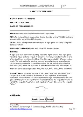
- 1. FUNDAMENTALS OF HDL LABORATORY MANUAL 2019 Prepared By: Mr. Omkar H. Darekar, Dept. of Electronics Engg. , AISSMS COE, Pune (MS) omkar.darekar.55@gmail.com Page 285 PRACTICE EXPERIMENT __________________________________________________ NAME :- Omkar H. Darekar ROLL NO :- 17EX310 DATE OF PERFORMANCE:- __________________________________________________ TITLE: Synthesis and Simulation of all Basic Logic Gates AIM : To design all Basic Logic gates. Realize them by writing VERILOG code and simulate all by using Xilinx ISE simulator. OBJECTIVES: To implement different types of logic gates and verify using test- bench waveform. EQUIPMENTS REQUIRED: PC with Xilinx ISE Software loaded THEORY: A logic gate is an elementary building block of a digital circuit. Most logic gates have two inputs and one output. At any given moment, every terminal is in one of the two binary conditions low (0) or high (1), represented by different voltage levels. The logic state of a terminal can, and generally does, change often, as the circuit processes data. In most logic gates, the low state is approximately zero volts (0 V), while the high state is approximately five volts positive (+5 V). There are seven basic logic gates: AND, OR, XOR, NOT, NAND, NOR, and XNOR. The AND gate is so named because, if 0 is called "false" and 1 is called "true," the gate acts in the same way as the logical "and" operator. The following illustration and table show the circuit symbol and logic combinations for an AND gate. (In the symbol, the input terminals are at left and the output terminal is at right.) The output is "true" when both inputs are "true." Otherwise, the output is "false." AND gate Input 1 Input 2 Output
- 2. FUNDAMENTALS OF HDL LABORATORY MANUAL 2019 Prepared By: Mr. Omkar H. Darekar, Dept. of Electronics Engg. , AISSMS COE, Pune (MS) omkar.darekar.55@gmail.com Page 286 0 0 0 0 1 0 1 0 0 1 1 1 The OR gate gets its name from the fact that it behaves after the fashion of the logical inclusive "or." The output is "true" if either or both of the inputs are "true." If both inputs are "false," then the output is "false." OR gate Input 1 Input 2 Output 0 0 0 0 1 1 1 0 1 1 1 1 The XOR ( exclusive-OR ) gate acts in the same way as the logical "either/or." The output is "true" if either, but not both, of the inputs are "true." The output is "false" if both inputs are "false" or if both inputs are "true." Another way of looking at this circuit is to observe that the output is 1 if the inputs are different, but 0 if the inputs are the same. XOR gate Input 1 Input 2 Output
- 3. FUNDAMENTALS OF HDL LABORATORY MANUAL 2019 Prepared By: Mr. Omkar H. Darekar, Dept. of Electronics Engg. , AISSMS COE, Pune (MS) omkar.darekar.55@gmail.com Page 287 0 0 0 0 1 1 1 0 1 1 1 0 A logical inverter, sometimes called a NOT gate to differentiate it from other types of electronic inverter devices, has only one input. It reverses the logic state. Inverter or NOT gate The NAND gate operates as an AND gate followed by a NOT gate. It acts in the manner of the logical operation "and" followed by negation. The output is "false" if both inputs are "true." Otherwise, the output is "true." NAND gate Input 1 Input 2 Output 0 0 1 0 1 1 1 0 1 1 1 0 The NOR gate is a combination OR gate followed by an inverter. Its output is "true" if both inputs are "false." Otherwise, the output is "false." Input Output 1 0 0 1
- 4. FUNDAMENTALS OF HDL LABORATORY MANUAL 2019 Prepared By: Mr. Omkar H. Darekar, Dept. of Electronics Engg. , AISSMS COE, Pune (MS) omkar.darekar.55@gmail.com Page 288 NOR gate Input 1 Input 2 Output 0 0 1 0 1 0 1 0 0 1 1 0 The XNOR (exclusive-NOR) gate is a combination XOR gate followed by an inverter. Its output is "true" if the inputs are the same, and"false" if the inputs are different. XNOR gate Input 1 Input 2 Output 0 0 1 0 1 0 1 0 0 1 1 1 Using combinations of logic gates, complex operations can be performed. In theory, there is no limit to the number of gates that can be arrayed together in a single device. But in practice, there is a limit to the number of gates that can be packed into a given physical space. Arrays of logic gates are found in digital integrated circuits (ICs). As IC technology advances, the required physical volume for each individual logic gate decreases and digital devices of the same or smaller size become capable of performing evermore-complicated operations at ever-increasing speeds.
- 5. FUNDAMENTALS OF HDL LABORATORY MANUAL 2019 Prepared By: Mr. Omkar H. Darekar, Dept. of Electronics Engg. , AISSMS COE, Pune (MS) omkar.darekar.55@gmail.com Page 289 Logic block diagram: Truth Table: Input2 Input 1 Y_AND Y_OR Y_NOT (1) Y_NOT (2) Y_NAND Y_NOR Y_XOR Y_XNOR 0 0 0 0 1 1 1 1 0 1 0 1 0 1 0 1 1 0 1 0 1 0 0 1 1 0 1 0 1 0 1 1 1 1 0 0 0 0 0 1 VERILOG CODE: module all_gates(a, b, and_y, or_y, not_y, nand_y, xor_y, xnor_y, nor_y); input a; input b; output and_y; output or_y; output not_y; output nand_y; output xor_y; output xnor_y; output nor_y; assign and_y= a & b; assign or_y=a| b; Input 1 Input 2 text Outputs Y _ OR Y _ AND Y _ NOT Y _ NAND Y _ NOR Y _ XOR Y _ XNOR Basic Logic Gates
- 6. FUNDAMENTALS OF HDL LABORATORY MANUAL 2019 Prepared By: Mr. Omkar H. Darekar, Dept. of Electronics Engg. , AISSMS COE, Pune (MS) omkar.darekar.55@gmail.com Page 290 assign not_y=~ b; assign nand_y=~(a&b); assign xor_y=a ^ b; assign xnor_y=~(a ^ b); assign nor_y=~(a | b); endmodule
- 7. FUNDAMENTALS OF HDL LABORATORY MANUAL 2019 Prepared By: Mr. Omkar H. Darekar, Dept. of Electronics Engg. , AISSMS COE, Pune (MS) omkar.darekar.55@gmail.com Page 291 RTL SCHEMATIC:
- 8. FUNDAMENTALS OF HDL LABORATORY MANUAL 2019 Prepared By: Mr. Omkar H. Darekar, Dept. of Electronics Engg. , AISSMS COE, Pune (MS) omkar.darekar.55@gmail.com Page 292
- 9. FUNDAMENTALS OF HDL LABORATORY MANUAL 2019 Prepared By: Mr. Omkar H. Darekar, Dept. of Electronics Engg. , AISSMS COE, Pune (MS) omkar.darekar.55@gmail.com Page 293 TECHNOLOGY SCHEMATIC: LUT 2_8: And Gate
- 10. FUNDAMENTALS OF HDL LABORATORY MANUAL 2019 Prepared By: Mr. Omkar H. Darekar, Dept. of Electronics Engg. , AISSMS COE, Pune (MS) omkar.darekar.55@gmail.com Page 294 LUT 2_7 : Nand Gate LUT 2_1: Nor Gate LUT 2_E: Or Gate
- 11. FUNDAMENTALS OF HDL LABORATORY MANUAL 2019 Prepared By: Mr. Omkar H. Darekar, Dept. of Electronics Engg. , AISSMS COE, Pune (MS) omkar.darekar.55@gmail.com Page 295 LUT 2_9: XNor Gate LUT 2_6: XOr Gate
- 12. FUNDAMENTALS OF HDL LABORATORY MANUAL 2019 Prepared By: Mr. Omkar H. Darekar, Dept. of Electronics Engg. , AISSMS COE, Pune (MS) omkar.darekar.55@gmail.com Page 296 Result : Design Summary :
- 13. FUNDAMENTALS OF HDL LABORATORY MANUAL 2019 Prepared By: Mr. Omkar H. Darekar, Dept. of Electronics Engg. , AISSMS COE, Pune (MS) omkar.darekar.55@gmail.com Page 297 EXPERIMENT NO. 9 __________________________________________________ NAME :- Omkar H. Darekar ROLL NO :- 17EX310 DATE OF PERFORMANCE:- __________________________________________________ TITLE: Synthesis and Simulation of Half add/sub and full add/sub AIM : To design Half Adder and Subtractor and Full Adder and Subtractor. Realize them by writing Verilog code and simulate all by using Xilinx ISE simulator. OBJECTIVES: To implement combinational logic gates (Half Adder and Subtractor and Full Adder and Subtractor) and verify using test-bench waveform. EQUIPMENTS REQUIRED: PC with Xilinx ISE Software loaded INTRODUCTION: The half adder adds two one-bit binary numbers A and B. It has two outputs, S and C (the value theoretically carried on to the next addition); the final sum is 2C + S. The simplest half-adder design, pictured on the right, incorporates an XOR ate for S and an AND gate for C. With the addition of an OR gate to combine their carry outputs, two half adders can be combined to make a full adder. In this lab, you will learn how to implement an Half Adder using Xilinx ISE Tool. � Write the functionality in the Xilinx project navigator. � Run a functional HDL simulation. � Synthesize your design with XST.
- 14. FUNDAMENTALS OF HDL LABORATORY MANUAL 2019 Prepared By: Mr. Omkar H. Darekar, Dept. of Electronics Engg. , AISSMS COE, Pune (MS) omkar.darekar.55@gmail.com Page 298 � Take the synthesized design through the Xilinx implementation tools. � Check the performance of your design by applying different inputs and verify the outputs using simulator THEORY: Half adder is a combinational arithmetic circuit that adds two numbers and produces a sum bit (S) and carry bit (C) as the output. If A and B are the input bits, then sum bit (S) is the X-OR of A and B and the carry bit (C) will be the AND of A and B. From this it is clear that a half adder circuit can be easily constructed using one X-OR gate and one AND gate. Half adder is the simplest of all adder circuit, but it has a major disadvantage. The half adder can add only two input bits (A and B) and has nothing to do with the carry if there is any in the input. So if the input to a half adder have a carry, then it will be neglected it and adds only the A and B bits. That means the binary addition process is not complete and that‟s why it is called a half adder. DESIGN DESCRIPTION: Adds two 1-bit operands, producing a 2-bit output. The low-order bit of the output is called as ‟Sum‟ while the higher-order bit is called as „Carry‟. Logic block diagram:
- 15. FUNDAMENTALS OF HDL LABORATORY MANUAL 2019 Prepared By: Mr. Omkar H. Darekar, Dept. of Electronics Engg. , AISSMS COE, Pune (MS) omkar.darekar.55@gmail.com Page 299 Truth Table: LOGIC GATE CIRCUIT: BOOLEAN EQUATION:-
- 16. FUNDAMENTALS OF HDL LABORATORY MANUAL 2019 Prepared By: Mr. Omkar H. Darekar, Dept. of Electronics Engg. , AISSMS COE, Pune (MS) omkar.darekar.55@gmail.com Page 300 VERILOG CODE: HALF ADDER: Structural model Dataflow model Behavioural model modulehalfaddstr(sum,carry,a,b); outputsum,carry; inputa,b; xor(sum,a,b); and(carry,a,b); endmodule modulehalfadddf(sum,carry,a,b); outputsum,carry; inputa,b; assign sum = a^b; assign carry=a&b; endmodule modulehalfaddbeh(sum,carry,a,b); outputsum,carry; inputa,b; regsum,carry; always@(a,b); sum = a^b; carry=a&b; endmodule
- 17. FUNDAMENTALS OF HDL LABORATORY MANUAL 2019 Prepared By: Mr. Omkar H. Darekar, Dept. of Electronics Engg. , AISSMS COE, Pune (MS) omkar.darekar.55@gmail.com Page 301 RTL SCHEMATIC:
- 18. FUNDAMENTALS OF HDL LABORATORY MANUAL 2019 Prepared By: Mr. Omkar H. Darekar, Dept. of Electronics Engg. , AISSMS COE, Pune (MS) omkar.darekar.55@gmail.com Page 302 TECHNOLOGY SCHEMATIC: LUT 2_8 LUT 2_6
- 19. FUNDAMENTALS OF HDL LABORATORY MANUAL 2019 Prepared By: Mr. Omkar H. Darekar, Dept. of Electronics Engg. , AISSMS COE, Pune (MS) omkar.darekar.55@gmail.com Page 303 SIMULATION : DESIGN SUMMARY:
- 20. FUNDAMENTALS OF HDL LABORATORY MANUAL 2019 Prepared By: Mr. Omkar H. Darekar, Dept. of Electronics Engg. , AISSMS COE, Pune (MS) omkar.darekar.55@gmail.com Page 304 HALF SUBTRACTOR: INTRODUCTION: The half subtractor subtracts two one-bit binary numbers A and B. It has two outputs, D and B (the value theoretically carried on to the next subtraction); the final difference is 2b - d. The simplest half-subtracter design, pictured on the right, incorporates an XOR gate for D and an AND gate and NOT gate for B. With the addition of an OR gate to combine their borrow outputs, two half subtractor can be combined to make a full subtractor. In this lab, you will learn how to implement an Half subtractor using Xilinx ISE Tool. � Write the functionality in the Xilinx project navigator. � Run a functional HDL simulation. � Synthesize your design with XST. � Take the synthesized design through the Xilinx implementation tools. � Check the performance of your design by applying different inputs and verify the outputs using simulator DESIGN DESCRIPTION: Subtracts two 1-bit operands, producing a 2-bit output. The low-order bit of the output is called as ‟Difference‟ while the higher-order bit is called as „Borrow‟. LOGIC BLOCK DIAGRAM:
- 21. FUNDAMENTALS OF HDL LABORATORY MANUAL 2019 Prepared By: Mr. Omkar H. Darekar, Dept. of Electronics Engg. , AISSMS COE, Pune (MS) omkar.darekar.55@gmail.com Page 305 TRUTH TABLE: LOGIC GATE CIRCUIT: Boolean Equation:
- 22. FUNDAMENTALS OF HDL LABORATORY MANUAL 2019 Prepared By: Mr. Omkar H. Darekar, Dept. of Electronics Engg. , AISSMS COE, Pune (MS) omkar.darekar.55@gmail.com Page 306 Verilog CODE: HALF SUBTRACTOR: Structural model Dataflow model Behavioural model modulehalfsubtstr(diff,borrow,a,b); outputdiff,borrow; inputa,b; xor(diff,a,b); and (borrow,~a,b); endmodule modulehalfsubtdf(diff,borrow,a,b); outputdiff,borrow; inputa,b; assign diff = a^b; assign borrow=(~a&b); endmodule modulehalfsubtbeh(diff,borrow,a,b); outputdiff,borrow; inputa,b; regdiff,borrow; always@(a,b); diff= a^b; borrow=(~a&b) endmodule
- 23. FUNDAMENTALS OF HDL LABORATORY MANUAL 2019 Prepared By: Mr. Omkar H. Darekar, Dept. of Electronics Engg. , AISSMS COE, Pune (MS) omkar.darekar.55@gmail.com Page 307 RTL SCHEMATIC: 1
- 24. FUNDAMENTALS OF HDL LABORATORY MANUAL 2019 Prepared By: Mr. Omkar H. Darekar, Dept. of Electronics Engg. , AISSMS COE, Pune (MS) omkar.darekar.55@gmail.com Page 308 TECHNOLOGY SCHEMATIC:
- 25. FUNDAMENTALS OF HDL LABORATORY MANUAL 2019 Prepared By: Mr. Omkar H. Darekar, Dept. of Electronics Engg. , AISSMS COE, Pune (MS) omkar.darekar.55@gmail.com Page 309 SIMULATION: DESIGN SUMMARY:
- 26. FUNDAMENTALS OF HDL LABORATORY MANUAL 2019 Prepared By: Mr. Omkar H. Darekar, Dept. of Electronics Engg. , AISSMS COE, Pune (MS) omkar.darekar.55@gmail.com Page 310 Full adder: The main difference between a half-adder and a full-adder is that the full-adder has three inputs and two outputs. The first two inputs are A and B and the third input is an input carry designated as CIN. When full adder logic is designed we will be able to string eight of them together to create a byte-wide adder and cascade the carry bit from one adder to the next. INTRODUCTION: Addition of two binary digits is most basic operation performed by digital computers. In many computers and other kinds of processors, adders are used not only in Arithmetic Logic Units(ALU) but also in other parts of processor, where they are used to calculate addresses, table indices and similar. Although adders can be constructed for many numerical representations such as binary coded decimal or Excess 3, the most common adders operate on binary numbers. Adders can be modified as subtractions using 1‟s and 2‟s complement.A full adder circuit is an arithmetic circuit block that can be used to add three bits to produce a SUM and a CARRY output. Such a building block becomes a necessity when it comes to adding binary numbers with a large number of bits. The full adder circuit overcomes the limitation of the half-adder, which can be used to add two bits only. In this lab, you will learn how to implement an full Adder using Xilinx ISE Tool. � Write the functionality in the Xilinx project navigator. � Run a functional HDL simulation. � Synthesize your design with XST. � Take the synthesized design through the Xilinx implementation tools. � Check the performance of your design by applying different inputs and verify the outputs using simulator.
- 27. FUNDAMENTALS OF HDL LABORATORY MANUAL 2019 Prepared By: Mr. Omkar H. Darekar, Dept. of Electronics Engg. , AISSMS COE, Pune (MS) omkar.darekar.55@gmail.com Page 311 DESIGN DESCRIPTION: The procedure for adding larger binary numbers, begin with the addition of LSBs of the two numbers. We record the sum under the LSB column and take the carry, if any, forward to the next higher column bits. As a result, when we add the next adjacent higher column bits, we would be required to add three bits if there were a carry from the previous addition. We have a similar situation for the other higher column bits . LOGIC BLOCK DIAGRAM:
- 28. FUNDAMENTALS OF HDL LABORATORY MANUAL 2019 Prepared By: Mr. Omkar H. Darekar, Dept. of Electronics Engg. , AISSMS COE, Pune (MS) omkar.darekar.55@gmail.com Page 312 TRUTH TABLE: INPUT OUTPUTS A B Cin SUM CARRY 0 0 0 0 0 0 0 1 1 0 0 1 0 1 0 0 1 1 0 1 1 0 0 1 0 1 0 1 0 1 1 1 0 0 1 1 1 1 1 1 LOGIC GATE CIRCUIT: Using nand gates :
- 29. FUNDAMENTALS OF HDL LABORATORY MANUAL 2019 Prepared By: Mr. Omkar H. Darekar, Dept. of Electronics Engg. , AISSMS COE, Pune (MS) omkar.darekar.55@gmail.com Page 313 Using Half-Adders: Boolean equations: VERILOG CODE: FULL ADDER: Structural model Dataflow model Behavioural model modulefulladdstr(sum,carry,a,b); outputsum,carry; inputa,b,c; xor g1(sum,a,b,c); and g2(x,a,b); and g3(y,b,c); and g3(z,c,a); or g5(carry,x,y,z); endmodule modulefulladddf(sum,carry,a,b); outputsum,carry; inputa,b,c; assign sum = a^b^c; assign carry=(a&b) | (b&c) | (c&a); endmodule modulefulladdbeh(sum,carry,a,b); outputsum,carry; inputa,b,c; regsum,carry; always@(a,b,c); sum = a^b^c; carry=a&b|(b&c)|(c&a)|; endmodule
- 30. FUNDAMENTALS OF HDL LABORATORY MANUAL 2019 Prepared By: Mr. Omkar H. Darekar, Dept. of Electronics Engg. , AISSMS COE, Pune (MS) omkar.darekar.55@gmail.com Page 314 RTL SCHEMATIC:
- 31. FUNDAMENTALS OF HDL LABORATORY MANUAL 2019 Prepared By: Mr. Omkar H. Darekar, Dept. of Electronics Engg. , AISSMS COE, Pune (MS) omkar.darekar.55@gmail.com Page 315 TECHNOLOGY SCHEMATIC:
- 32. FUNDAMENTALS OF HDL LABORATORY MANUAL 2019 Prepared By: Mr. Omkar H. Darekar, Dept. of Electronics Engg. , AISSMS COE, Pune (MS) omkar.darekar.55@gmail.com Page 316
- 33. FUNDAMENTALS OF HDL LABORATORY MANUAL 2019 Prepared By: Mr. Omkar H. Darekar, Dept. of Electronics Engg. , AISSMS COE, Pune (MS) omkar.darekar.55@gmail.com Page 317 SIMULATION: DESIGN SUMMARY:
- 34. FUNDAMENTALS OF HDL LABORATORY MANUAL 2019 Prepared By: Mr. Omkar H. Darekar, Dept. of Electronics Engg. , AISSMS COE, Pune (MS) omkar.darekar.55@gmail.com Page 318 FULL SUBTRACTOR: Subtraction of two binary digits is most basic operation performed by digital computers. In many computers and other kinds of processors, subtractors are used not only in Arithmetic Logic Units(ALU) but also in other parts of processor. A full subtractor circuit is an arithmetic circuit block that can be used to subtract three bits to produce a DIFFERENCE and a BORROW output. Such a building block becomes a necessity when it comes to subtracting binary numbers with a large number of bits. In this lab, you will learn how to implement an full subtractor using Xilinx ISE Tool. � Write the functionality in the Xilinx project navigator. � Run a functional HDL simulation. � Synthesize your design with XST. � Take the synthesized design through the Xilinx implementation tools. � Check the performance of your design by applying different inputs and verify the outputs using simulator. LOGIC BLOCK DIAGRAM:
- 35. FUNDAMENTALS OF HDL LABORATORY MANUAL 2019 Prepared By: Mr. Omkar H. Darekar, Dept. of Electronics Engg. , AISSMS COE, Pune (MS) omkar.darekar.55@gmail.com Page 319 TRUTH TABLE: LOGIC GATE CIRCUIT: BOOLEAN EQUATION:
- 36. FUNDAMENTALS OF HDL LABORATORY MANUAL 2019 Prepared By: Mr. Omkar H. Darekar, Dept. of Electronics Engg. , AISSMS COE, Pune (MS) omkar.darekar.55@gmail.com Page 320 VERILOG CODE: FULL SUBTRACTOR: Structural model Dataflow model Behavioural model module fullsubtstr(diff,borrow,a,b,c); outputdiff,borrow; inputa,b,c; wire a0,q,r,s,t; not(a0,a); xor(x,a,b); xor(diff,x,c); and (y,a0,b); and(z,~x,c); or(borrow,y,z); endmodule modulefullsubtdf(diff,borrow,a,b,c); outputdiff,borrow; inputa,b,c; assign diff = a^b^c; assign borrow=(~a&b)|(~(a^b)&c) ; endmodule modulefullsubtbeh(diff,borrow,a,b,c); outputdiff,borrow; inputa,b,c; outputdiff,borrow; always@(a,b); diff= a^b^c; borrow=(~a&b)|(~(a^b)&c); endmodule
- 37. FUNDAMENTALS OF HDL LABORATORY MANUAL 2019 Prepared By: Mr. Omkar H. Darekar, Dept. of Electronics Engg. , AISSMS COE, Pune (MS) omkar.darekar.55@gmail.com Page 321 RTL SCHEMATIC:
- 38. FUNDAMENTALS OF HDL LABORATORY MANUAL 2019 Prepared By: Mr. Omkar H. Darekar, Dept. of Electronics Engg. , AISSMS COE, Pune (MS) omkar.darekar.55@gmail.com Page 322 TECHNOLOGY:
- 39. FUNDAMENTALS OF HDL LABORATORY MANUAL 2019 Prepared By: Mr. Omkar H. Darekar, Dept. of Electronics Engg. , AISSMS COE, Pune (MS) omkar.darekar.55@gmail.com Page 323 SIMULATION: DESIGN SUMMARY
- 40. FUNDAMENTALS OF HDL LABORATORY MANUAL 2019 Prepared By: Mr. Omkar H. Darekar, Dept. of Electronics Engg. , AISSMS COE, Pune (MS) omkar.darekar.55@gmail.com Page 324 EXPERIMENT NO. 10 NAME :- Omkar H. Darekar ROLL NO :- 17EX310 DATE OF PERFORMANCE:- TITLE:SYNTHESIS AND SIMULATION OF 8:1 MULTIPLEXER USING VERILOG AIM: DRAW THE LOGIC BLOCK, TRUTHTABLE AND LOGIC GATE CIRCUIT OF 8:1 MULTIPLEXER. WRITE THE VERILOG PROGRAM CODE. SIMULATE IT USING XILINX ISE TOOL VERSION 9.2i. INTRODUCTION: The Multiplexer is a combinational circuit that is the most widely used circuit in Digital Design. Multiplexing means transmitting a large number of information units over a smaller number of channels or lines. A Digital Multiplexer is a combinational circuit that selects binary information from one of many input lines and directs it to a single output line. The selection of a particular input line is controlled by a set of selection lines. In this lab, you will learn how to implement an 8:1 Multiplexer using Xilinx ISE Tool. Write the functionality in the Xilinx project navigator. Run a functional HDL simulation. Synthesize your design with XST. Take the synthesized design through the Xilinx implementation tools. Check the performance of your design by applying different inputs and verify the outputs using simulator tool .
- 41. FUNDAMENTALS OF HDL LABORATORY MANUAL 2019 Prepared By: Mr. Omkar H. Darekar, Dept. of Electronics Engg. , AISSMS COE, Pune (MS) omkar.darekar.55@gmail.com Page 325 THEORY: The multiplexer, shortened to “MUX”, is a combinational logic circuit designed to switch one of several input lines through to a single common output line by the application of a control signal. Multiplexers operate like very fast acting multiple position rotary switches connecting or controlling multiple input lines called “channels” one at a time to the output. Multiplexers, or MUX‟s, can be either digital circuits made from high speed logic gates used to switch digital or binary data or they can be analogue types using transistors, MOSFET‟s or relays to switch one of the voltage or current inputs through to a single output. In digital electronics, multiplexers are also known as data selectors because they can “select” each input line, are constructed from individual Analogue Switches encased in a single IC package as opposed to the “mechanical” Generally, the selection of each input line in a multiplexer is controlled by an additional set of inputs called control lines and according to the binary condition of these control inputs, either “HIGH” or “LOW” the appropriate data input is connected directly to the output. Normally, a multiplexer has an even number of 2n data input lines and a number of “control” inputs that correspond with the number of data inputs. Note that multiplexers are different in operation to Encoders. Encoders are able to switch an n-bit inputpattern to multiple output lines that represent the binary coded (BCD) output equivalent of the active input.
- 42. FUNDAMENTALS OF HDL LABORATORY MANUAL 2019 Prepared By: Mr. Omkar H. Darekar, Dept. of Electronics Engg. , AISSMS COE, Pune (MS) omkar.darekar.55@gmail.com Page 326 For a 8-input multiplexer we would therefore require three data select lines as 8-inputs represents 23 data control lines give a circuit with 8 inputs,D0,D1,D2,D3, D4, D5, D6, D7 and 3 data select lines S0,S1and S2 as shown. OBJECTIVES: After completing this lab, you will be able to implement the multiplexer in FPGA and verify it. DESIGN DESCRIPTION: For selecting one out of „n‟ inputs for connection to the output, a set of m select inputs are required. 2m = n (n= Number of inputs, m = Number of select lines) Depending upon the digital code applied at the select inputs one out of 8 data sources is selected & transmitted to a single output Channel. LOGIC BLOCK DIAGRAM: SEL DATA OUTPUT D0 D1 D2 DN -1 YMULTIPLEXER SELECT N DATA SOURCES / INPUTS BITS BITS BITS BITS BITS BITS 8:1 MULTIPLEXER
- 43. FUNDAMENTALS OF HDL LABORATORY MANUAL 2019 Prepared By: Mr. Omkar H. Darekar, Dept. of Electronics Engg. , AISSMS COE, Pune (MS) omkar.darekar.55@gmail.com Page 327 TRUTH TABLE: S2 S1 S0 Y 0 0 0 D0 0 0 1 D1 0 1 0 D2 0 1 1 D3 1 0 0 D4 1 0 1 D5 1 1 0 D6 1 1 1 D7 LOGIC SYMBOL:
- 44. FUNDAMENTALS OF HDL LABORATORY MANUAL 2019 Prepared By: Mr. Omkar H. Darekar, Dept. of Electronics Engg. , AISSMS COE, Pune (MS) omkar.darekar.55@gmail.com Page 328 LOGIC GATE CIRCUIT: 8:1 MULTIPLEXER
- 45. FUNDAMENTALS OF HDL LABORATORY MANUAL 2019 Prepared By: Mr. Omkar H. Darekar, Dept. of Electronics Engg. , AISSMS COE, Pune (MS) omkar.darekar.55@gmail.com Page 329 VERILOG CODE: module mux_3x8(in,out,sel); input [7:0]in; input [2:0]sel; output out; reg out; wire [2:0]sel; wire [7:0]in; always @(sel or in) begin if (sel==0) out = in[0]; elsif (sel==1) out = in[1]; elsif (sel==2) out = in[2]; elsif (sel==3) out = in[3]; elsif (sel==4) out = in[4]; elsif (sel==5) out = in[5];
- 46. FUNDAMENTALS OF HDL LABORATORY MANUAL 2019 Prepared By: Mr. Omkar H. Darekar, Dept. of Electronics Engg. , AISSMS COE, Pune (MS) omkar.darekar.55@gmail.com Page 330 elsif (sel==6) out = in[6]; else out = in[7]; end endmodule
- 47. FUNDAMENTALS OF HDL LABORATORY MANUAL 2019 Prepared By: Mr. Omkar H. Darekar, Dept. of Electronics Engg. , AISSMS COE, Pune (MS) omkar.darekar.55@gmail.com Page 331 RTL SCHEMATIC:
- 48. FUNDAMENTALS OF HDL LABORATORY MANUAL 2019 Prepared By: Mr. Omkar H. Darekar, Dept. of Electronics Engg. , AISSMS COE, Pune (MS) omkar.darekar.55@gmail.com Page 332 TECHNOLOGY SCHEMATIC: LUT3_E4:
- 49. FUNDAMENTALS OF HDL LABORATORY MANUAL 2019 Prepared By: Mr. Omkar H. Darekar, Dept. of Electronics Engg. , AISSMS COE, Pune (MS) omkar.darekar.55@gmail.com Page 333
- 50. FUNDAMENTALS OF HDL LABORATORY MANUAL 2019 Prepared By: Mr. Omkar H. Darekar, Dept. of Electronics Engg. , AISSMS COE, Pune (MS) omkar.darekar.55@gmail.com Page 334 SIMULATION:
- 51. FUNDAMENTALS OF HDL LABORATORY MANUAL 2019 Prepared By: Mr. Omkar H. Darekar, Dept. of Electronics Engg. , AISSMS COE, Pune (MS) omkar.darekar.55@gmail.com Page 335 II-MODELLING STYLE: STRUCTURAL Structural Verilog code of 8:1 mux module mux2to1(a,b,sel,out); input a,b,sel; output out; tri out; bufif1 (out,a,sel); bufif0 (out,b,sel); endmodule module mux4to1(a,sel,out); input [3:0] a; input [1:0] sel; output out; wire mux[2:0]; mux2to1 m1 (a[3],a[2],sel[0],mux_1), m2 (a[1],a[4],sel[0],mux_2),
- 52. FUNDAMENTALS OF HDL LABORATORY MANUAL 2019 Prepared By: Mr. Omkar H. Darekar, Dept. of Electronics Engg. , AISSMS COE, Pune (MS) omkar.darekar.55@gmail.com Page 336 m3 (mux_1,mux_2,sel[1],out); endmodule module mux8to1(a,sel,out); input [7:0] a; input [2:0] sel; output out; wire mux[2:0]; mux4to1 m1 (a[7:4],sel[1:0],mux_1), m2 (a[3:0],sel[1:0],mux_2); mux2to1 m3 (mux_1,mux_2,sel[2],out); endmodule
- 53. FUNDAMENTALS OF HDL LABORATORY MANUAL 2019 Prepared By: Mr. Omkar H. Darekar, Dept. of Electronics Engg. , AISSMS COE, Pune (MS) omkar.darekar.55@gmail.com Page 337 DESIGN SUMMARY:
- 54. FUNDAMENTALS OF HDL LABORATORY MANUAL 2019 Prepared By: Mr. Omkar H. Darekar, Dept. of Electronics Engg. , AISSMS COE, Pune (MS) omkar.darekar.55@gmail.com Page 338 EXPERIMENT NO. 11 __________________________________________________ NAME :- Omkar H. Darekar ROLL NO :- 17EX310 DATE OF PERFORMANCE:- TITLE:SYNTHESIS AND SIMULATION OF 3:8 DECODER USING VERILOG AIM: DRAW THE LOGIC BLOCK, TRUTHTABLE AND LOGIC GATE CIRCUIT OF 3:8 DECODER. WRITE THE VERILOG PROGRAM CODE. SIMULATE IT USING XILINX ISE TOOL VERSION 9.2i. INTRODUCTION: Discrete quantities of information are represented in digital systems with binary codes. A binary code of n bits is capable of representing up to 2n distinct elements of the coded information. A Decoder is a combinational circuit that converts binary information from n input lines to a maximum of 2n unique output lines. Decoder is similar to a De- multiplexer except that there is no data input. The only inputs are the control inputs A, B and C. In this lab, you will learn how to implement a 3:8 Decoder using Xilinx ISE Tool. Write the functionality in the Xilinx project navigator. Run a functional HDL simulation. Synthesize your design with XST. Take the synthesized design through the Xilinx implementation tools. Check the performance of your design by applying binary inputs and verify the outputs.
- 55. FUNDAMENTALS OF HDL LABORATORY MANUAL 2019 Prepared By: Mr. Omkar H. Darekar, Dept. of Electronics Engg. , AISSMS COE, Pune (MS) omkar.darekar.55@gmail.com Page 339 Theory: In digital electronics, a decoder can take the form of a multiple- input, multiple-output logic circuit that converts coded inputs into coded outputs, where the input and output codes are different e.g. n-to-2n , binary-coded decimal decoders. Decoding is necessary in applications such as data multiplexing, 7 segment display and memory address decoding. The example decoder circuit would be an AND gate because the output of an AND gate is "High" (1) only when all its inputs are "High." Such output is called as "active High output". If instead of AND gate, the NAND gate is connected the output will be "Low" (0) only when all its inputs are "High". Such output is called as "active low output". A slightly more complex decoder would be the n-to-2n type binary decoders. These types of decoders are combinational circuits that convert binary information from 'n' coded inputs to a maximum of 2n unique outputs. In case the 'n' bit coded information has unused bit combinations, the decoder may have less than 2n outputs. 2-to-4 decoder, 3-to-8 decoder or 4-to-16 decoder are other examples. The input to a decoder is parallel binary number and it is used to detect the presence of a particular binary number at the input. The output indicates presence or absence of specific number at the decoder input. 3:8 decoder It uses all AND gates, and therefore, the outputs are active- high. For active- low outputs, NAND gates are used. It has 3 input lines and 8 output lines. It is also called as binary to octal decoder it takes a 3-bit binary input code and activates one of the 8(octal) outputs corresponding to that code.
- 56. FUNDAMENTALS OF HDL LABORATORY MANUAL 2019 Prepared By: Mr. Omkar H. Darekar, Dept. of Electronics Engg. , AISSMS COE, Pune (MS) omkar.darekar.55@gmail.com Page 340 OBJECTIVES: After completing this lab, you will be able to implement the Decoder in FPGA and verify it on Spartan-II / Spartan-III Protoboard. DESIGN DESCRIPTION: A binary decoder has n inputs and 2n outputs. Only one output is active at any one time, corresponding to the input value. LOGIC BLOCK DIAGRAM:
- 57. FUNDAMENTALS OF HDL LABORATORY MANUAL 2019 Prepared By: Mr. Omkar H. Darekar, Dept. of Electronics Engg. , AISSMS COE, Pune (MS) omkar.darekar.55@gmail.com Page 341 TRUTH TABLE: Z Y X F7 F6 F5 F4 F3 F2 F1 F0 0 0 0 0 0 0 0 0 0 0 1 0 0 1 0 0 0 0 0 0 1 0 0 1 0 0 0 0 0 0 1 0 0 0 1 1 0 0 0 0 1 0 0 0 1 0 0 0 0 0 1 0 0 0 0 1 0 1 0 0 1 0 0 0 0 0 1 1 0 0 1 0 0 0 0 0 0 1 1 1 1 0 0 0 0 0 0 0 LOGIC SYMBOL: 3:8 DECODER X Y Z F0 F1 F2 F3 F4 F5 F6 F7 LOGIC GATE CIRCUIT:
- 58. FUNDAMENTALS OF HDL LABORATORY MANUAL 2019 Prepared By: Mr. Omkar H. Darekar, Dept. of Electronics Engg. , AISSMS COE, Pune (MS) omkar.darekar.55@gmail.com Page 342 Y X Z F7 F6 F5 F4 F3 F2 F1 F0 3:8 Decoder
- 59. FUNDAMENTALS OF HDL LABORATORY MANUAL 2019 Prepared By: Mr. Omkar H. Darekar, Dept. of Electronics Engg. , AISSMS COE, Pune (MS) omkar.darekar.55@gmail.com Page 343 VERILOG CODE: Structural model Data Flow model Behavioural Model module decoder38str(z0,z1,z2,z3,z4,z5,z6,z7,a0, a1,a2); output z0,z1,z2,z3,z4,z5,z6,z7; input a0,a1,a2; not(s0,a0); not(s1,a1); not(s2,a2); and(z0,s1,s1,s2); and(z1,a0,s1,s2); and (z2,s0,a1,s2); and(z3,a0,a1,s2); and(z4,s0,s1,a2); and(z5,a0,s1,a2); and(z6,s0,a1,a2); and(z7,a0,a1,a2); endmodule Module decoder38df(z,a0,a1, a2); Output [7:0] z; Input a0,a1,a2; Assign z[0]=~a0&~a1 &~a2; Assign z[1]=~a0&~a1&a2; Assign z[2]=~a0& a1&~a2; Assign z[3]=~a0&a1&a2; Assign z[4]=a0&~a1&~a2; Assign z[5]= a0&~a1&a2; Assign z[6]=a0&a1& ~a2; Assign z[7]=a0&a17a2; endmodule Module decoder38beh(sel,out1 ): Input[2:0]sel; Outputreg[7:0]out1; Always @(sel.out1) Case(sel) 3`b000:out1=8`b00000 001; 3`b001:out1=8’b00000 010; 3`b010:out1=8’b00000 100; 3`b011:out1=8’b00001 000; 3`b100:out1=8’b00010 000; 3`b101:out1=8’b00100 000; 3`b110:out1=8’b01000 000; default:out1=8’b00000 000; endcase endmodule
- 60. FUNDAMENTALS OF HDL LABORATORY MANUAL 2019 Prepared By: Mr. Omkar H. Darekar, Dept. of Electronics Engg. , AISSMS COE, Pune (MS) omkar.darekar.55@gmail.com Page 344 RTL :
- 61. FUNDAMENTALS OF HDL LABORATORY MANUAL 2019 Prepared By: Mr. Omkar H. Darekar, Dept. of Electronics Engg. , AISSMS COE, Pune (MS) omkar.darekar.55@gmail.com Page 345 TECHNOLOGY:
- 62. FUNDAMENTALS OF HDL LABORATORY MANUAL 2019 Prepared By: Mr. Omkar H. Darekar, Dept. of Electronics Engg. , AISSMS COE, Pune (MS) omkar.darekar.55@gmail.com Page 346 SIMULATION: DESIGN SUMMARY:
- 63. FUNDAMENTALS OF HDL LABORATORY MANUAL 2019 Prepared By: Mr. Omkar H. Darekar, Dept. of Electronics Engg. , AISSMS COE, Pune (MS) omkar.darekar.55@gmail.com Page 347 Experiment No:12 __________________________________________________ NAME :- Omkar H. Darekar ROLL NO :- 17EX310 DATE OF PERFORMANCE:- __________________________________________________ TITLE: SYNTHESIS AND SIMULATION OF COMPARATOR USING VERILOG AIM: DRAW THE LOGIC BLOCK, TRUTHTABLE AND LOGIC GATE CIRCUIT OF COMPARATOR. WRITE THE VERILOG PROGRAM CODE. ALSO WRITE TEST BENCH WAVEFORM CODE. SIMULATE IT USING XILINX ISE TOOL VERSION 9.2i. INTRODUCTION: Digital comparator, also called as magnitude comparator is a combinational circuit, designed to compare the two n-bit binary words applied at its input. They are commonly used in devices such as analog-to-digital convertors (ADCs). In order to determine whether A is greater than or less than B, we inspect the relative magnitude of pairs of significant digits, starting from the most significant position. The comparison is done by successively comparing the next adjacent lower pair of digits if the digits of the pair under examination are equal. The comparison continues until a pair of unequal digits is reached. In this lab, you will learn how to implement a comparator using Xilinx ISE Tool. Write the functionality in the Xilinx project navigator. Run a functional HDL simulation.
- 64. FUNDAMENTALS OF HDL LABORATORY MANUAL 2019 Prepared By: Mr. Omkar H. Darekar, Dept. of Electronics Engg. , AISSMS COE, Pune (MS) omkar.darekar.55@gmail.com Page 348 Synthesize your design with XST. Take the synthesized design through the Xilinx implementation tools. Check the performance of your design by applying binary inputs and verify the outputs. THEORY: Digital or Binary Comparators are made up from standard AND, NORand NOT gates that compare the digital signals present at their input terminals and produce an output depending upon the condition of those inputs. For example, along with being able to add and subtract binary numbers we need to be able to compare them and determine whether the value of input A is greater than, smaller than or equal to the value at input B etc. The digital comparator accomplishes this using several logic gates that operate on the principles of Boolean algebra. There are two main types of Digital Comparatoravailable and these are. 1. Identity Comparator - an Identity Comparator is a digital comparator that has only one output terminal for when A = B either "HIGH"• A = B = 1 or "LOW"• A = B = 0 2. Magnitude Comparator - a Magnitude Comparator is a type of digital comparator that has three output terminals, one each for equality, A = B greater than, A > B and less thanA< B The purpose of a Digital Comparator is to compare a set of variables or unknown numbers, for example A (A1, A2, A3... An, etc.) .Against that of a constant or unknown value such as B (B1, B2, B...Bn,etc.) and produce an output condition or flag depending upon the result of the comparison. For example, a magnitude comparator of two 1-bits, (A and B) inputs would produce the following three output conditions when compared to each other.
- 65. FUNDAMENTALS OF HDL LABORATORY MANUAL 2019 Prepared By: Mr. Omkar H. Darekar, Dept. of Electronics Engg. , AISSMS COE, Pune (MS) omkar.darekar.55@gmail.com Page 349 A>B,A=B,A Which means: A is greater than B, A is equal to B, and A is less than B OBJECTIVES: After completing this lab, you will be able to implement the comparator in FPGA and verify it on Spartan-II / Spartan-III Protoboard. DESIGN DESCRIPTION: The comparator has three outputs namely A>B, A<B and A=B .Depending on result of comparison one of these outputs will go high. LOGIC BLOCK DIAGRAM: TRUTH TABLE: INPUTS OUTPUTS A B Y2<=A<B Y1<=A=B Y0<=A>B 0 0 0 1 0 0 1 1 0 0 1 0 0 0 1 1 1 0 1 0 N-BIT MAGNITUDE COMPARATOR n n Y
- 66. FUNDAMENTALS OF HDL LABORATORY MANUAL 2019 Prepared By: Mr. Omkar H. Darekar, Dept. of Electronics Engg. , AISSMS COE, Pune (MS) omkar.darekar.55@gmail.com Page 350 LOGIC GATE CIRCUIT: VERILOG CODE: module comp_ve1(a, b, equal, greater, lesser); input a; input b; outputequal; output greater; output lesser; wire s1, s2; not X1(s1, a); not X2 (s2, b); and X3 (le,s1, b); and X4 (gr,s2, a); xnor X5 (eq, a, b); endmodule
- 67. FUNDAMENTALS OF HDL LABORATORY MANUAL 2019 Prepared By: Mr. Omkar H. Darekar, Dept. of Electronics Engg. , AISSMS COE, Pune (MS) omkar.darekar.55@gmail.com Page 351 RTL :
- 68. FUNDAMENTALS OF HDL LABORATORY MANUAL 2019 Prepared By: Mr. Omkar H. Darekar, Dept. of Electronics Engg. , AISSMS COE, Pune (MS) omkar.darekar.55@gmail.com Page 352 TECHNOLOGY:
- 69. FUNDAMENTALS OF HDL LABORATORY MANUAL 2019 Prepared By: Mr. Omkar H. Darekar, Dept. of Electronics Engg. , AISSMS COE, Pune (MS) omkar.darekar.55@gmail.com Page 353 SIMULATION: DESIGN SUMMARY:
- 70. FUNDAMENTALS OF HDL LABORATORY MANUAL 2019 Prepared By: Mr. Omkar H. Darekar, Dept. of Electronics Engg. , AISSMS COE, Pune (MS) omkar.darekar.55@gmail.com Page 354 Experiment No:13 __________________________________________________ NAME :- Omkar H. Darekar ROLL NO :- 17EX310 DATE OF PERFORMANCE:- __________________________________________________ TITLE: SYNTHESIS AND SIMULATION OF SEVEN SEGMENT DISPLAY DECODER INTERFACE USING VERILOG AIM: DRAW THE LOGIC BLOCK, TRUTHTABLE AND LOGIC GATE CIRCUIT OF BCD TO SEVEN SEGMENT DECODER. WRITE THE VERILOG PROGRAM CODE. ALSO WRITE TEST BENCH WAVEFORM CODE. SIMULATE IT USING XILINX ISE TOOL VERSION 9.2i. INTRODUCTION: A display decoder is used to convert a BCD or a binary code into a 7 segment code used to operate a 7 segment LED display. It generally has 4 input lines and 7 output lines. Here we design a simple display decoder circuit using logic gates. Even though commercial BCD to 7 segment decoders are available, designing a display decoder using logic gates may prove to be beneficial from economical as well as knowledge point of view. In this lab, you will learn how to implement an BCD TO SEVEN SEGMENT DECODER using Xilinx ISE Tool. Write the functionality in the Xilinx project navigator. Run a functional HDL simulation. Synthesize your design with XST. Take the synthesized design through the Xilinx implementation tools.
- 71. FUNDAMENTALS OF HDL LABORATORY MANUAL 2019 Prepared By: Mr. Omkar H. Darekar, Dept. of Electronics Engg. , AISSMS COE, Pune (MS) omkar.darekar.55@gmail.com Page 355 Check the performance of your design by applying different inputs and verify the outputs. OBJECTIVES: After completing this lab, you will be able to implement the bcd to seven segment decoder in FPGA and verify it on Spartan-II / Spartan-III Protoboard. DESIGN DESCRIPTION: A 7 segment LED display consists of an arrangement of 8 LEDs such that either all the anodes are common or cathodes are common. A common cathode 7 segment display consists of 8 pins – 7 input pins labeled from „a‟ to „g‟ and 8th pin as common ground pin. LOGIC BLOCK DIAGRAM:
- 72. FUNDAMENTALS OF HDL LABORATORY MANUAL 2019 Prepared By: Mr. Omkar H. Darekar, Dept. of Electronics Engg. , AISSMS COE, Pune (MS) omkar.darekar.55@gmail.com Page 356 TRUTH TABLE: COMMON CATHODE
- 73. FUNDAMENTALS OF HDL LABORATORY MANUAL 2019 Prepared By: Mr. Omkar H. Darekar, Dept. of Electronics Engg. , AISSMS COE, Pune (MS) omkar.darekar.55@gmail.com Page 357 TRUTH TABLE: COMMON ANODE LOGIC GATE CIRCUIT:
- 74. FUNDAMENTALS OF HDL LABORATORY MANUAL 2019 Prepared By: Mr. Omkar H. Darekar, Dept. of Electronics Engg. , AISSMS COE, Pune (MS) omkar.darekar.55@gmail.com Page 358 VERILOG CODE: Behavioral Verilog Code for 7-Segment Decoder Input[3:0]bcd; Output[6:0]seg; Reg[6:0]seg; always@(bcd) begin case(bcd) 0:seg=7‟b0000001; 1:seg=7‟b1001111; 2:seg=7‟b0010010; 3:seg=7‟b0000110; 4:seg=7‟b1001100; 5:seg=7‟b0100100; 6:seg=7‟b0100000; 7:seg=7‟b0001111; 8:seg=7‟b0000000; 9:seg=7‟b0000100; default:seg=7‟b1111111; endcase end end module
- 75. FUNDAMENTALS OF HDL LABORATORY MANUAL 2019 Prepared By: Mr. Omkar H. Darekar, Dept. of Electronics Engg. , AISSMS COE, Pune (MS) omkar.darekar.55@gmail.com Page 359 Structural Verilog Code for 7-Segment Decoder: module bcd ( input i0, i1, i2, i3, output a, b, c, d, e, f, g ); wire ip0,ip1,ip2,a1,b1,d1,d2,d3,d4,e1,e2,f1,f2,f3,g1,g2; // first parameter is the output; remaining parameters are the inputs not U0(ip0,i0); not U1(ip1,i1); not U2(ip2,i2); xnor U3(a1,i2,i0); or U4(a,i3,i1,a1); xnor U5(b1,i1,i0); or U6(b,ip2,b1); or U7(c,i2,ip1,i0); and U8(d1,i1,ip0); and U9(d2,ip2,ip0); and U10(d3,ip2,i1); and U11(d4,i2,ip1,i0); or U12(d,d1,d2,d3,d4); and U13(e1,i1,ip0); and U14(e2,ip2,ip0); or U15(e,e1,e2); and U16(f1,i2,ip1);
- 76. FUNDAMENTALS OF HDL LABORATORY MANUAL 2019 Prepared By: Mr. Omkar H. Darekar, Dept. of Electronics Engg. , AISSMS COE, Pune (MS) omkar.darekar.55@gmail.com Page 360 and U17(f2,i2,ip0); and U18(f3,ip1,ip0); or U19(f,i3,f1,f2,f3); xor U20(g1,i2,i1); and U21(g2,i1,ip0); or U22(g,i3,g1,g2); endmodule Dataflow Verilog Code for 7-Segment Decoder module bcd ( input i0, i1, i2, i3, output a, b, c, d, e, f, g ); assign a = i3 | i1 | (i2 ~^ i0); // bitwise ~=NOT; &=AND; |=OR; ^=XOR assign b = ~i2 | ~(i1 ^ i0); assign c = i2 | ~i1 | i0; assign d = (i1 & ~i0) | (~i2 & ~i0) | (~i2 & i1) | (i2 & ~i1 & i0); assign e = (i1 & ~i0) | (~i2 & ~i0); assign f = i3 | (i2 & ~i1) | (i2 & ~i0) | (~i1 & ~i0) | (i2 & ~i0) | (~i1 & ~i0); assign g = i3 | (i2 ^ i1) | (i1 & ~i0); endmodule
- 77. FUNDAMENTALS OF HDL LABORATORY MANUAL 2019 Prepared By: Mr. Omkar H. Darekar, Dept. of Electronics Engg. , AISSMS COE, Pune (MS) omkar.darekar.55@gmail.com Page 361 RTL :
- 78. FUNDAMENTALS OF HDL LABORATORY MANUAL 2019 Prepared By: Mr. Omkar H. Darekar, Dept. of Electronics Engg. , AISSMS COE, Pune (MS) omkar.darekar.55@gmail.com Page 362 TECHNOLOGY:
- 79. FUNDAMENTALS OF HDL LABORATORY MANUAL 2019 Prepared By: Mr. Omkar H. Darekar, Dept. of Electronics Engg. , AISSMS COE, Pune (MS) omkar.darekar.55@gmail.com Page 363 SIMULATION: DESIGN SUMMARY:
- 80. FUNDAMENTALS OF HDL LABORATORY MANUAL 2019 Prepared By: Mr. Omkar H. Darekar, Dept. of Electronics Engg. , AISSMS COE, Pune (MS) omkar.darekar.55@gmail.com Page 364 Experiment No:14 __________________________________________________ NAME :- Omkar H. Darekar ROLL NO :- 17EX310 DATE OF PERFORMANCE:- __________________________________________________ TITLE: SYNTHESIS AND SIMULATION OF DIFFERENT TYPES OF FLIPFLOPS AIM: DRAW THE LOGIC BLOCK, TRUTHTABLE AND LOGIC GATE CIRCUIT OF ALL FLIPFLOPS. WRITE THE VERILOG PROGRAM CODE. SIMULATE IT USING XILINX ISE TOOL VERSION 9.2i. THEORY: Flip flops are actually an application of logic gates. With the help of Boolean logic you can create memory with them. Flip flops can also be considered as the most basic idea of a Random Access Memory [RAM]. When a certain input value is given to them, they will be remembered and executed, if the logic gates are designed correctly. A higher application of flip flops is helpful in designing better electronic circuits. The most commonly used application of flip flops is in the implementation of a feedback circuit. As a memory relies on the feedback concept, flip flops can be used to design it. There are mainly four types of flip flops that are used in electronic circuits. They are 1. The basic Flip Flop or S-R Flip Flop 2. Delay Flip Flop [D Flip Flop] 3. J-K Flip Flop 4. T Flip Flop
- 81. FUNDAMENTALS OF HDL LABORATORY MANUAL 2019 Prepared By: Mr. Omkar H. Darekar, Dept. of Electronics Engg. , AISSMS COE, Pune (MS) omkar.darekar.55@gmail.com Page 365 INTRODUCTION: 1. S-R FlipFlop The SET-RESET flip flop is designed with the help of two NOR gates and also two NAND gates. These flip flops are also called S-R Latch. S-R Flip Flop using NOR Gate The design of such a flip flop includes two inputs, called the SET [S] and RESET [R]. There are also two outputs, Q and Q‟. LOGIC GATE CIRCUIT: TRUTH TABLE: S R Q Q’ 0 0 0 1 0 1 0 1 1 0 1 0 1 1 ∞ ∞
- 82. FUNDAMENTALS OF HDL LABORATORY MANUAL 2019 Prepared By: Mr. Omkar H. Darekar, Dept. of Electronics Engg. , AISSMS COE, Pune (MS) omkar.darekar.55@gmail.com Page 366 VERILOG CODE: SR modulesrff(q,q1,r,s,clk); output q,q1; inputr,s,clk; reg q,q1; initial begin q=1'b0; q1=1'b1; end always @(posedgeclk) begin case({s,r}) {1'b0,1'b0}: begin q=q; q1=q1; end {1'b0,1'b1}: begin q=1'b0; q1=1'b1; end {1'b1,1'b0}: begin q=1'b1; q1=1'b0; end {1'b1,1'b1}: begin q=1'bx; q=1'bx; end endcase end endmodule
- 83. FUNDAMENTALS OF HDL LABORATORY MANUAL 2019 Prepared By: Mr. Omkar H. Darekar, Dept. of Electronics Engg. , AISSMS COE, Pune (MS) omkar.darekar.55@gmail.com Page 367 RTL:
- 84. FUNDAMENTALS OF HDL LABORATORY MANUAL 2019 Prepared By: Mr. Omkar H. Darekar, Dept. of Electronics Engg. , AISSMS COE, Pune (MS) omkar.darekar.55@gmail.com Page 368 TECHNOLOGY:
- 85. FUNDAMENTALS OF HDL LABORATORY MANUAL 2019 Prepared By: Mr. Omkar H. Darekar, Dept. of Electronics Engg. , AISSMS COE, Pune (MS) omkar.darekar.55@gmail.com Page 369 SIMULATION: DESIGN SUMMARY:
- 86. FUNDAMENTALS OF HDL LABORATORY MANUAL 2019 Prepared By: Mr. Omkar H. Darekar, Dept. of Electronics Engg. , AISSMS COE, Pune (MS) omkar.darekar.55@gmail.com Page 370 2. D Flip Flop A D flip-flop is also called a delay flip-flop. Itcan be used to provide temporary storage of one bit of information. When the clock is enabled, the binary data present at the D input is transferred to the Q output. D flip- flop is obtained from RS flip-flop by applying D input directly to S input and its complement is applied to R input. This ensures that S and R are never equal to 1 at the same time and eliminates the undesirable condition of the indeterminate state in RS flip-flop. A flip-flop is a bistable multivibrator. The circuit can be made to change state by signals applied to one or more control inputs and will have one or two outputs. It is the basic storage element in sequential logic. Flip-flops and latches are a fundamental building block of digital electronics systems used in computers, communications, and many other types of systems. DESIGN DESCRIPTION: D input is sampled when clk=1. If D=1, output goes 1, placing the circuit in the set state. If D=0, output goes to 0 and the circuit switches to clear state. But if clk=0, output retains the previous value and is independent of changes in D input. LOGIC BLOCK DIAGRAM:
- 87. FUNDAMENTALS OF HDL LABORATORY MANUAL 2019 Prepared By: Mr. Omkar H. Darekar, Dept. of Electronics Engg. , AISSMS COE, Pune (MS) omkar.darekar.55@gmail.com Page 371 LOGIC SYMBOL: TRUTH TABLE: clk D Q (n+1) 0 0 0 1 0 0 1 1 1 LOGIC GATE CIRCUIT: D FLIP FLOP (NAND_GATES) LOGIC GATE CIRCUIT:
- 88. FUNDAMENTALS OF HDL LABORATORY MANUAL 2019 Prepared By: Mr. Omkar H. Darekar, Dept. of Electronics Engg. , AISSMS COE, Pune (MS) omkar.darekar.55@gmail.com Page 372 VERILOG CODE: moduleuy(q, q_bar, clk, d); output q; outputq_bar; input clk; input d; nand U1(x,d,clk); nand U2(y,x,clk); nand U3(q,q_bar,x); nand U4(q_bar,q,y); endmodule
- 89. FUNDAMENTALS OF HDL LABORATORY MANUAL 2019 Prepared By: Mr. Omkar H. Darekar, Dept. of Electronics Engg. , AISSMS COE, Pune (MS) omkar.darekar.55@gmail.com Page 373 RTL
- 90. FUNDAMENTALS OF HDL LABORATORY MANUAL 2019 Prepared By: Mr. Omkar H. Darekar, Dept. of Electronics Engg. , AISSMS COE, Pune (MS) omkar.darekar.55@gmail.com Page 374 TECHNOLOGY
- 91. FUNDAMENTALS OF HDL LABORATORY MANUAL 2019 Prepared By: Mr. Omkar H. Darekar, Dept. of Electronics Engg. , AISSMS COE, Pune (MS) omkar.darekar.55@gmail.com Page 375 SIMULATION DESIGN SUMMARY
- 92. FUNDAMENTALS OF HDL LABORATORY MANUAL 2019 Prepared By: Mr. Omkar H. Darekar, Dept. of Electronics Engg. , AISSMS COE, Pune (MS) omkar.darekar.55@gmail.com Page 376 3. J-K Flip Flop A J-K flip flop can also be defined as a modification of the S-R flip flop. The only difference is that the intermediate state is more refined and precise than that of a S-R flip flop.1 The behavior of inputs J and K is same as the S and R inputs of the S-R flip flop. The letter J stands for SET and the letter K stands for CLEAR. DESIGN DESCRIPTION: This simple JK flip Flop is the most widely used of all the flip-flop designs and is considered to be a universal flip-flop circuit. It has 2 inputs J and K depending on their values output level Q changes. It has 2 more inputs preset and clear. The JK flip flop is basically a gated SR flip-flop with the addition of a clock input circuitry that prevents the illegal or invalid output condition that can occur when both inputs S and R are equal to logic level “1”. Due to this additional clocked input, a JK flip-flop has four possible input combinations, “logic 1”, “logic 0”, “no change” and “toggle”. The symbol for a JK flip flop is similar to that of an SR BISTABLE LATCH as seen in the previous tutorial except for the addition of a clock input. LOGIC BLOCK DIAGRAM: The input condition of J=K=1, gives an output inverting the output state. However, the outputs are same when one tests the circuit practically.
- 93. FUNDAMENTALS OF HDL LABORATORY MANUAL 2019 Prepared By: Mr. Omkar H. Darekar, Dept. of Electronics Engg. , AISSMS COE, Pune (MS) omkar.darekar.55@gmail.com Page 377 TRUTH TABLE: LOGIC GATE CIRCUIT: VERILOG CODE: moduleJK_flip_flop ( j ,k ,clk ,reset ,q ,qb ); output q ; reg q ; outputqb ; regqb ; input j ;
- 94. FUNDAMENTALS OF HDL LABORATORY MANUAL 2019 Prepared By: Mr. Omkar H. Darekar, Dept. of Electronics Engg. , AISSMS COE, Pune (MS) omkar.darekar.55@gmail.com Page 378 wire j ; input k ; wire k ; inputclk ; wireclk ; input reset ; wire reset ; always @ (posedge (clk)) begin if (reset) begin q <= 0; qb<= 1; end else begin if (j!=k) begin q <= j; qb<= k; end else if (j==1 && k==1) begin q <= ~q; qb<= ~qb; end end end endmodule
- 95. FUNDAMENTALS OF HDL LABORATORY MANUAL 2019 Prepared By: Mr. Omkar H. Darekar, Dept. of Electronics Engg. , AISSMS COE, Pune (MS) omkar.darekar.55@gmail.com Page 379 RTL
- 96. FUNDAMENTALS OF HDL LABORATORY MANUAL 2019 Prepared By: Mr. Omkar H. Darekar, Dept. of Electronics Engg. , AISSMS COE, Pune (MS) omkar.darekar.55@gmail.com Page 380 TECHNOLOGY
- 97. FUNDAMENTALS OF HDL LABORATORY MANUAL 2019 Prepared By: Mr. Omkar H. Darekar, Dept. of Electronics Engg. , AISSMS COE, Pune (MS) omkar.darekar.55@gmail.com Page 381 SIMULATION DESIGN SUMMARY
- 98. FUNDAMENTALS OF HDL LABORATORY MANUAL 2019 Prepared By: Mr. Omkar H. Darekar, Dept. of Electronics Engg. , AISSMS COE, Pune (MS) omkar.darekar.55@gmail.com Page 382 4. T Flip Flop This is a much simpler version of the J-K flip flop. Both the J and K inputs are connected together and thus are also called a single input J-K flip flop. When clock pulse is given to the flip flop, the output begins to toggle. Here also the restriction on the pulse width can be eliminated with a master-slave or edge- triggered construction.The T flip-flop has one input in addition to the clock. T stands for toggle for the obvious reason. When T is asserted (T = 1), the flip-flop state toggles back and forth, and when T is de-asserted, the flip-flop keeps its current state. The T flip-flop can be constructed using a D flip-flop with the two outputs Q and ' feedback to the D input through a multiplexer that is controlled by the T input DESIGN DESCRIPTION: When T=0, Q (t+1) =Q. That is next state is same as present state and no change occurs. When T=1, then Q (t+1 =Q‟ and the state of flip-flop is complemented. LOGIC BLOCK DIAGRAM: Truth Table: Clk T Q+ 0 0 0 0 1 1 1 1 0 1 1 1
- 99. FUNDAMENTALS OF HDL LABORATORY MANUAL 2019 Prepared By: Mr. Omkar H. Darekar, Dept. of Electronics Engg. , AISSMS COE, Pune (MS) omkar.darekar.55@gmail.com Page 383 LOGIC CIRCUIT DIAGRAM: Verilog CODE: module t_flip_flop ( t ,clk ,q,qb ); output q; reg q ; output qb; reg qb ; input t ; wire t ; input clk ; wire clk ; initial dout = 0; always @ (posedge (clk)) begin if (reset) dout <= 0; else begin if (t) q <= ~q; end end endmodul
- 100. FUNDAMENTALS OF HDL LABORATORY MANUAL 2019 Prepared By: Mr. Omkar H. Darekar, Dept. of Electronics Engg. , AISSMS COE, Pune (MS) omkar.darekar.55@gmail.com Page 384 RTL
- 101. FUNDAMENTALS OF HDL LABORATORY MANUAL 2019 Prepared By: Mr. Omkar H. Darekar, Dept. of Electronics Engg. , AISSMS COE, Pune (MS) omkar.darekar.55@gmail.com Page 385 TECHNOLOGY
- 102. FUNDAMENTALS OF HDL LABORATORY MANUAL 2019 Prepared By: Mr. Omkar H. Darekar, Dept. of Electronics Engg. , AISSMS COE, Pune (MS) omkar.darekar.55@gmail.com Page 386 SIMULATION DESIGN SUMMARY
- 103. FUNDAMENTALS OF HDL LABORATORY MANUAL 2019 Prepared By: Mr. Omkar H. Darekar, Dept. of Electronics Engg. , AISSMS COE, Pune (MS) omkar.darekar.55@gmail.com Page 387 5.D-LATCH Latch is an electronic device that can be used to store one bit of information. The D latch is used to capture, or 'latch' the logic level which is present on the Data line when the clock input is high. If the data on the D line changes state while the clock pulse is high, then the output, Q, follows the input, D. When the CLK input falls to logic 0, the last state of the D input is trapped and held in the latch. Latches and flip-flops are the basic elements for storing information. One latch or flip-flop can store one bit of information. The main difference between latches and flip-flops is that for latches, their outputs are constantly affected by their inputs as long as the enable signal is asserted. In other words, when they are enabled, their content changes immediately when their inputs change. Flip-flops, on the other hand, have their content change only either at the rising or falling edge of the enable signal. This enable signal is usually the controlling clock signal. After the rising or falling edge of the clock, the flip-flop content remains constant even if the input changes. There are basically four main types of latches and flip-flops: SR, D, JK, and T. The major differences in these flip-flop types are the number of inputs they have and how they change state. Latches are level sensitive and transparent. DESIGN DESCRIPTION: D input is sampled when enable=1. If D=1, output goes 1, placing the circuit in the set state. If D=0, output goes to 0 and the circuit switches to clear state. But if clk=0, output retains the previous value and is independent of changes in D input. LOGIC BLOCK DIAGRAM: d- latch
- 104. FUNDAMENTALS OF HDL LABORATORY MANUAL 2019 Prepared By: Mr. Omkar H. Darekar, Dept. of Electronics Engg. , AISSMS COE, Pune (MS) omkar.darekar.55@gmail.com Page 388 LOGIC CIRCUIT DIAGRAM: Truth table: VERILOG CODE: module d_latch(q, qb, din, e); output q,qb; input din; input e; nand g1 (s, din, e), g2 (r, db, e); not g3 (db,din);
- 105. FUNDAMENTALS OF HDL LABORATORY MANUAL 2019 Prepared By: Mr. Omkar H. Darekar, Dept. of Electronics Engg. , AISSMS COE, Pune (MS) omkar.darekar.55@gmail.com Page 389 nand g4 (q, s, qb); nand g5 (qb , q); endmodule
- 106. FUNDAMENTALS OF HDL LABORATORY MANUAL 2019 Prepared By: Mr. Omkar H. Darekar, Dept. of Electronics Engg. , AISSMS COE, Pune (MS) omkar.darekar.55@gmail.com Page 390 RTL
- 107. FUNDAMENTALS OF HDL LABORATORY MANUAL 2019 Prepared By: Mr. Omkar H. Darekar, Dept. of Electronics Engg. , AISSMS COE, Pune (MS) omkar.darekar.55@gmail.com Page 391 TECHNOLOGY
- 108. FUNDAMENTALS OF HDL LABORATORY MANUAL 2019 Prepared By: Mr. Omkar H. Darekar, Dept. of Electronics Engg. , AISSMS COE, Pune (MS) omkar.darekar.55@gmail.com Page 392 SIMULATION DESIGN SUMMARY
- 109. FUNDAMENTALS OF HDL LABORATORY MANUAL 2019 Prepared By: Mr. Omkar H. Darekar, Dept. of Electronics Engg. , AISSMS COE, Pune (MS) omkar.darekar.55@gmail.com Page 393 6.UP-DOWN COUNTERS Counter is the most useful and versatile subsystem of digital branch. Counter is going to count number of clock pulses applied to it. Maximum count that binary counter can count is 2n - 1. Clock pulses occur at regular time interval, so that counter can be used to measure time or frequency. Digital counters are integrated circuits (ICs) that count events in computers and other digital systems. Because they must remember past states, digital counters include memory. Generally, digital counters consist of bistable devices or bistable multi vibrators called flip-flops. The number of flip-flops and the way in which they are connected determines the number of states and the sequence of states that digital counters complete in each full cycle. Counters can be subdivided into 2 groups: Asynchronous Counters Synchronous Counters The way in which devices are clocked determines whether digital counters are categorized as synchronous or asynchronous. In synchronous devices (such as synchronous BCD counters and synchronous decade counters), one clock triggers all of the flip-flops simultaneously. With asynchronous devices, often called asynchronous ripple counters an external clock pulse triggers only the first first-flop. Each successive flip-flop is then clocked by one of the outputs (Q or Q') of the previous flip-flop. Digital counters are configured as UP (counting in increasing sequence), DOWN (counting in decreasing sequence) or Bidirectional (UP / DOWN). DESIGN DESCRIPTION: It has the 2 i/ps one is clk and other is count. The o/p is obtained on the 4 bit o/p channel. count=count+1 if cnt=1 and count=count-1 if
- 110. FUNDAMENTALS OF HDL LABORATORY MANUAL 2019 Prepared By: Mr. Omkar H. Darekar, Dept. of Electronics Engg. , AISSMS COE, Pune (MS) omkar.darekar.55@gmail.com Page 394 cnt=0.For every rising edge of the clock the o/p increases or decreases by 1 depending on the value of cnt. LOGIC BLOCK DIAGRAM: TRUTH TABLE:
- 111. FUNDAMENTALS OF HDL LABORATORY MANUAL 2019 Prepared By: Mr. Omkar H. Darekar, Dept. of Electronics Engg. , AISSMS COE, Pune (MS) omkar.darekar.55@gmail.com Page 395 Sr. No. Mode control M Present state Next state D flip-flop inputs QD QC QB QA QD+1 QC+1 QB+1 QA+1 DD DC DB DA 0 0 0 0 0 0 0 0 0 1 0 0 0 1 1 0 0 0 0 1 0 0 1 0 0 0 1 0 2 0 0 0 1 0 0 0 1 1 0 0 1 1 3 0 0 0 1 1 0 1 0 0 0 1 0 0 4 0 0 1 0 0 0 1 0 1 0 1 0 1 5 0 0 1 0 1 0 1 1 0 0 1 1 0 6 0 0 1 1 0 0 1 1 1 0 1 1 1 7 0 0 1 1 1 1 0 0 0 1 0 0 0 8 0 1 0 0 0 1 0 0 1 1 0 0 1 9 0 1 0 0 1 1 0 1 0 1 0 1 0 10 0 1 0 1 0 1 0 1 1 1 0 1 1 11 0 1 0 1 1 1 1 0 0 1 1 0 0 12 0 1 1 0 0 1 1 0 1 1 1 0 1 13 0 1 1 0 1 1 1 1 0 1 1 1 0 14 0 1 1 1 0 1 1 1 1 1 1 1 1 15 0 1 1 1 1 0 0 0 0 0 0 0 0 16 1 0 0 0 0 1 1 1 1 1 1 1 1 17 1 0 0 0 1 0 0 0 0 0 0 0 0 18 1 0 0 1 0 0 0 0 1 0 0 0 1 19 1 0 0 1 1 0 0 1 0 0 0 1 0 20 1 0 1 0 0 0 0 1 1 0 0 1 1 21 1 0 1 0 1 0 1 0 0 0 1 0 0 22 1 0 1 1 0 0 1 0 1 0 1 0 1 23 1 0 1 1 1 0 1 1 0 0 1 1 0 24 1 1 0 0 0 0 1 1 1 0 1 1 1 25 1 1 0 0 1 1 0 0 0 1 0 0 0 26 1 1 0 1 0 1 0 0 1 1 0 0 1 27 1 1 0 1 1 1 0 1 0 1 0 1 0 28 1 1 1 0 0 1 0 1 1 1 0 1 1 29 1 1 1 0 1 1 1 0 0 1 1 0 0 30 1 1 1 1 0 1 1 0 1 1 1 0 1 31 1 1 1 1 1 1 1 1 0 1 1 1 0 U P C O U N T I N D O W N C O U N T I N
- 112. FUNDAMENTALS OF HDL LABORATORY MANUAL 2019 Prepared By: Mr. Omkar H. Darekar, Dept. of Electronics Engg. , AISSMS COE, Pune (MS) omkar.darekar.55@gmail.com Page 396 VERILOG CODE: module up_down_counter(op,up_down,load,enable,clk,rst_a); output [`width-1:0] op; input up_down; input load; input enable; input clk; input rst_a; reg [`width-1:0] tmp_ip; assign op=tmp_ip; always @(posedge clk,posedge rst_a) begin if(rst_a) tmp_ip=0; else begin if(load) tmp_ip=`ip; else begin if(enable) begin if (up_down)
- 113. FUNDAMENTALS OF HDL LABORATORY MANUAL 2019 Prepared By: Mr. Omkar H. Darekar, Dept. of Electronics Engg. , AISSMS COE, Pune (MS) omkar.darekar.55@gmail.com Page 397 tmp_ip=tmp_ip+1; else tmp_ip=tmp_ip-1; end end end end endmodule
- 114. FUNDAMENTALS OF HDL LABORATORY MANUAL 2019 Prepared By: Mr. Omkar H. Darekar, Dept. of Electronics Engg. , AISSMS COE, Pune (MS) omkar.darekar.55@gmail.com Page 398 RTL
- 115. FUNDAMENTALS OF HDL LABORATORY MANUAL 2019 Prepared By: Mr. Omkar H. Darekar, Dept. of Electronics Engg. , AISSMS COE, Pune (MS) omkar.darekar.55@gmail.com Page 399 TECHNOLOGY
- 116. FUNDAMENTALS OF HDL LABORATORY MANUAL 2019 Prepared By: Mr. Omkar H. Darekar, Dept. of Electronics Engg. , AISSMS COE, Pune (MS) omkar.darekar.55@gmail.com Page 400 SIMULATION DESIGN SUMMARY
- 117. FUNDAMENTALS OF HDL LABORATORY MANUAL 2019 Prepared By: Mr. Omkar H. Darekar, Dept. of Electronics Engg. , AISSMS COE, Pune (MS) omkar.darekar.55@gmail.com Page 401 Experiment No:15 __________________________________________________ NAME :- Omkar H. Darekar ROLL NO :- 17EX310 DATE OF PERFORMANCE:- TITLE: SYNTHESIS AND SIMULATION OF SHIFT REGISTERS AIM: DRAW THE LOGIC BLOCK, TRUTHTABLE AND LOGIC GATE CIRCUIT OF SERIAL AND PARALLEL REGISTER (SISO,SIPO,PIPO,PISO). WRITE THE VERILOG PROGRAM CODE. SIMULATE IT USING XILINX ISE TOOL VERSION 9.2i. THEORY: A Register is a very important digital building block.It is used to momentarily store binary information at the output of an encoding matrix. There are basically the four types viz; SISO,SIPO,PIPO,PISO etc. It uses the fliP-flops most widely use the D flip-flop as the memory element.On every clock trigger the registers changes the values. Registers is one of the basic application of flip-flops. Flip-flop is a 1-bit memory cell which can be used for storing digital data. To increase the storage capacity in terms of number of bits, we have to use group of flip-flops. Such a group of flip-flops is known as a register. Hence the n- bit register will consist of n number of flip-flops and is capable of storing n-bit word. A shift register is a storage device that used to store binary data. When a number of flip flop are connected in series it is called a register. A single flip flop is supposed to stay in one of the two stable states 1 or 0 or in other words the flip flop contains a number 1 or 0 depending upon the state in which it is. A register will thus contain a series of bits which can be termed as a word or byte. If in these registers the connection is
- 118. FUNDAMENTALS OF HDL LABORATORY MANUAL 2019 Prepared By: Mr. Omkar H. Darekar, Dept. of Electronics Engg. , AISSMS COE, Pune (MS) omkar.darekar.55@gmail.com Page 402 done in such a way that the output of one of the flip flop forms in input to other, it is known as a shift register. The data in a shift register is moved serially (one bit at a time). Shift registers can have both parallel and serial inputs and outputs. These are often configured as serial-in, parallel-out (SIPO) or as parallel-in, serial-out (PISO). There are also types that have both serial and parallel input and types with serial and parallel output. There are also bi-directional shift registers which allow shifting in both directions: L → R or R → L. The serial input and last output of a shift register can also be connected together to create a circular shift register. Data can be entered or taken out of the registers in serial (one bit at a time) or parallel (all the bits at a time) form. Based on this registers can be classified as: - Serial in serial out (SISO), serial in parallel out (SIPO), parallel in serial out (PISO) and parallel in parallel out (PIPO). Registers are also available in MSI devices. The shift register can be built using RS, JK or D flip-flops various types of shift registers are available. They are Shift Left Register, Shift Right Register. LOGIC BLOCK DIAGRAM:
- 119. FUNDAMENTALS OF HDL LABORATORY MANUAL 2019 Prepared By: Mr. Omkar H. Darekar, Dept. of Electronics Engg. , AISSMS COE, Pune (MS) omkar.darekar.55@gmail.com Page 403 LODIC SYMBOL: TRUTH TABLE: FOR SISO: CLK Q3 Q2=D3 Q1=D2 Q0=D1 SERIAL INPUT DIN=D0 Initially 0 0 0 0 1st 0 0 0 1 1 2nd 0 0 1 1 1 3rd 0 1 1 1 1 4th 1 1 1 1 1
- 120. FUNDAMENTALS OF HDL LABORATORY MANUAL 2019 Prepared By: Mr. Omkar H. Darekar, Dept. of Electronics Engg. , AISSMS COE, Pune (MS) omkar.darekar.55@gmail.com Page 404 VERILOG CODE: [FOR ALL SISO, SIPO, PIPO, PISO] VERILOG CODE FOR SISO: module siso(clk,rst,a,q); input a; input clk,rst; output q; reg q; always@(posedge clk,posedge rst) begin if(rst==1'b1) q<=1'b0; else q<=a; end endmodule
- 121. FUNDAMENTALS OF HDL LABORATORY MANUAL 2019 Prepared By: Mr. Omkar H. Darekar, Dept. of Electronics Engg. , AISSMS COE, Pune (MS) omkar.darekar.55@gmail.com Page 405 RTL FOR SISO:
- 122. FUNDAMENTALS OF HDL LABORATORY MANUAL 2019 Prepared By: Mr. Omkar H. Darekar, Dept. of Electronics Engg. , AISSMS COE, Pune (MS) omkar.darekar.55@gmail.com Page 406 TECHNOLOGY FOR SISO:
- 123. FUNDAMENTALS OF HDL LABORATORY MANUAL 2019 Prepared By: Mr. Omkar H. Darekar, Dept. of Electronics Engg. , AISSMS COE, Pune (MS) omkar.darekar.55@gmail.com Page 407 SIMULATION
- 124. FUNDAMENTALS OF HDL LABORATORY MANUAL 2019 Prepared By: Mr. Omkar H. Darekar, Dept. of Electronics Engg. , AISSMS COE, Pune (MS) omkar.darekar.55@gmail.com Page 408 VERILOG CODE FOR SIPO: module sipo(a,clk,rst,q); input clk,rst; input a; output [3:0]q; wire [3:0]q; reg [3:0]temp; always@(posedge clk,posedge rst) begin if(rst==1'b1) temp<=4'b0000; else begin temp<=temp<<1'b1; temp[0]<=a; end end assign q=temp; endmodule
- 125. FUNDAMENTALS OF HDL LABORATORY MANUAL 2019 Prepared By: Mr. Omkar H. Darekar, Dept. of Electronics Engg. , AISSMS COE, Pune (MS) omkar.darekar.55@gmail.com Page 409 RTL FOR SIPO:
- 126. FUNDAMENTALS OF HDL LABORATORY MANUAL 2019 Prepared By: Mr. Omkar H. Darekar, Dept. of Electronics Engg. , AISSMS COE, Pune (MS) omkar.darekar.55@gmail.com Page 410 TECHNOLOGY SIMULATION
- 127. FUNDAMENTALS OF HDL LABORATORY MANUAL 2019 Prepared By: Mr. Omkar H. Darekar, Dept. of Electronics Engg. , AISSMS COE, Pune (MS) omkar.darekar.55@gmail.com Page 411
- 128. FUNDAMENTALS OF HDL LABORATORY MANUAL 2019 Prepared By: Mr. Omkar H. Darekar, Dept. of Electronics Engg. , AISSMS COE, Pune (MS) omkar.darekar.55@gmail.com Page 412 VERILOG CODE FOR PIPO: module pipo(clk,rst,a,q); input clk,rst; input[3:0]a; output[3:0]q; reg[3:0]q; always@(posedge clk,posedge rst) begin if (rst==1'b1) q<=4'b0000; else q<=a; end endmodule
- 129. FUNDAMENTALS OF HDL LABORATORY MANUAL 2019 Prepared By: Mr. Omkar H. Darekar, Dept. of Electronics Engg. , AISSMS COE, Pune (MS) omkar.darekar.55@gmail.com Page 413 RTL
- 130. FUNDAMENTALS OF HDL LABORATORY MANUAL 2019 Prepared By: Mr. Omkar H. Darekar, Dept. of Electronics Engg. , AISSMS COE, Pune (MS) omkar.darekar.55@gmail.com Page 414 TECHNOLOGY
- 131. FUNDAMENTALS OF HDL LABORATORY MANUAL 2019 Prepared By: Mr. Omkar H. Darekar, Dept. of Electronics Engg. , AISSMS COE, Pune (MS) omkar.darekar.55@gmail.com Page 415 SIMULATION
- 132. FUNDAMENTALS OF HDL LABORATORY MANUAL 2019 Prepared By: Mr. Omkar H. Darekar, Dept. of Electronics Engg. , AISSMS COE, Pune (MS) omkar.darekar.55@gmail.com Page 416 VERILOG CODE FOR PISO: module piso(clk,rst,a,q); input clk,rst; input [3:0]a; output q; reg q; reg [3:0]temp; always@(posedge clk,posedge rst) begin if(rst==1'b1) begin q<=1'b0; temp<=a; end else begin q<=temp[0]; temp <= temp>>1'b1; end end endmodule
- 133. FUNDAMENTALS OF HDL LABORATORY MANUAL 2019 Prepared By: Mr. Omkar H. Darekar, Dept. of Electronics Engg. , AISSMS COE, Pune (MS) omkar.darekar.55@gmail.com Page 417 RTL
- 134. FUNDAMENTALS OF HDL LABORATORY MANUAL 2019 Prepared By: Mr. Omkar H. Darekar, Dept. of Electronics Engg. , AISSMS COE, Pune (MS) omkar.darekar.55@gmail.com Page 418 TECHNOLOGY
- 135. FUNDAMENTALS OF HDL LABORATORY MANUAL 2019 Prepared By: Mr. Omkar H. Darekar, Dept. of Electronics Engg. , AISSMS COE, Pune (MS) omkar.darekar.55@gmail.com Page 419 SIMULATION DESIGN SUMMARY
- 136. FUNDAMENTALS OF HDL LABORATORY MANUAL 2019 Prepared By: Mr. Omkar H. Darekar, Dept. of Electronics Engg. , AISSMS COE, Pune (MS) omkar.darekar.55@gmail.com Page 420 Shift Left Register: A four stage shift-left register is shown below. The individual stages are JK flip flops. Notice that the data input consists of opposite binary signals, the reference data signal going to the J input and the opposite data signal going to the K input. For the D-type stage the single data input line is connected as the D-input. Block Diagram The shift pulse is applied to each stage operating each simultaneously. When the shift pulse occurs the data input is shifted in to that stage. Each stage is set or reset corresponding to the input data at the time the shift pulse occurs. Thus the input data bit is shift into stage A by the first shift pulse. At the same time the data of stage A is shifted into the stage B and so on for the following stages. At each shift pulse data stored in the register stages shifts left by one stage. New data shifted into stage A, whereas the data present in stage D is shifted out to the left for use by some other shift register or computer unit. For example consider starting with all stages reset all Q-outputs to logical 0 and applying steady logical 1 input as sata input stage A. table 1 show data in each stage after each of four shift pulses. Notice table 2 how the logical 1 input first shifts into stage A and then to stage D after four shift pulses.
- 137. FUNDAMENTALS OF HDL LABORATORY MANUAL 2019 Prepared By: Mr. Omkar H. Darekar, Dept. of Electronics Engg. , AISSMS COE, Pune (MS) omkar.darekar.55@gmail.com Page 421 As another example consider shifting alternate 0 and 1 data into stage A starting with all stages 1. Table 2 shows the data in each stage after each of four shift pulses. Finally as a third example of shift register operation, consider starting with the count in step 4 of table 2 and apply four more shift pulses with placing a steady logical 0 input as data input to stage A, table 3 shows this operation. Truth Table:
- 138. FUNDAMENTALS OF HDL LABORATORY MANUAL 2019 Prepared By: Mr. Omkar H. Darekar, Dept. of Electronics Engg. , AISSMS COE, Pune (MS) omkar.darekar.55@gmail.com Page 422 Shift Right Register : Sometimes it is necessary to shift the least significant digit first, as when addition is to be carried out serially. In that case a shift register is used as in figure 2 input data is applied to stage D and shifted right. Block Diagram
- 139. FUNDAMENTALS OF HDL LABORATORY MANUAL 2019 Prepared By: Mr. Omkar H. Darekar, Dept. of Electronics Engg. , AISSMS COE, Pune (MS) omkar.darekar.55@gmail.com Page 423 The shift operation is same as discussed in shift left register except that data transfers to the right. Table 4 shows the action of shifting all logical 1 inputs into an initially reset shift register. In addition to shifting data register, data into a register data is also a register. Table 5 shows register operation for an initial value of 1101. Notice that the output from stage A contains the binary number each bit (starting initially with LSB) appearing at the output of each shift step. In the present example it was assumed that logical 0 was shifted as input data so that after four shift pulses have occurred the data has passed through the register and the stages are left reset after the fourth shift pulse. VERILOG CODE: Shift left: Module test; Reg[3:0]x; Intial Begin X=4‟b1100 $display(“x before shift=%4b”,x); X=x<<1; $display(“x after shift=%4b”,x); end end module
- 140. FUNDAMENTALS OF HDL LABORATORY MANUAL 2019 Prepared By: Mr. Omkar H. Darekar, Dept. of Electronics Engg. , AISSMS COE, Pune (MS) omkar.darekar.55@gmail.com Page 424 RTL Shift Left:
- 141. FUNDAMENTALS OF HDL LABORATORY MANUAL 2019 Prepared By: Mr. Omkar H. Darekar, Dept. of Electronics Engg. , AISSMS COE, Pune (MS) omkar.darekar.55@gmail.com Page 425 TECHNOLOGY Left Shift:
- 142. FUNDAMENTALS OF HDL LABORATORY MANUAL 2019 Prepared By: Mr. Omkar H. Darekar, Dept. of Electronics Engg. , AISSMS COE, Pune (MS) omkar.darekar.55@gmail.com Page 426 SIMULATION Shift left:
- 143. FUNDAMENTALS OF HDL LABORATORY MANUAL 2019 Prepared By: Mr. Omkar H. Darekar, Dept. of Electronics Engg. , AISSMS COE, Pune (MS) omkar.darekar.55@gmail.com Page 427 CODE: Shift right: Module test; Reg[3:0]x; Intial Begin X=4‟b1100 $display(“x before shift=%4b”,x); X=x>>1; $display(“x after shift=%4b”,x); end end module
- 144. FUNDAMENTALS OF HDL LABORATORY MANUAL 2019 Prepared By: Mr. Omkar H. Darekar, Dept. of Electronics Engg. , AISSMS COE, Pune (MS) omkar.darekar.55@gmail.com Page 428 RTL Right Shift
- 145. FUNDAMENTALS OF HDL LABORATORY MANUAL 2019 Prepared By: Mr. Omkar H. Darekar, Dept. of Electronics Engg. , AISSMS COE, Pune (MS) omkar.darekar.55@gmail.com Page 429 TECHNOLOGY
- 146. FUNDAMENTALS OF HDL LABORATORY MANUAL 2019 Prepared By: Mr. Omkar H. Darekar, Dept. of Electronics Engg. , AISSMS COE, Pune (MS) omkar.darekar.55@gmail.com Page 430 SIMULATION Shift Right: DESIGN SUMMARY
- 147. FUNDAMENTALS OF HDL LABORATORY MANUAL 2019 Prepared By: Mr. Omkar H. Darekar, Dept. of Electronics Engg. , AISSMS COE, Pune (MS) omkar.darekar.55@gmail.com Page 431 EXPERIMENT NO:16 __________________________________________________ NAME :- Omkar H. Darekar ROLL NO :- 17EX310 DATE OF PERFORMANCE:- __________________________________________________ TITLE: Synthesis of ALU using VERILOG and simulate it. AIM :To design ALU (Arithmetic and logic unit) to Perform – ADD, SUB, AND, OR, 1‟s compliment, 2‟sCompliment, Multiplication and Division. INTRODUCTION: The ALU is the core component of all microprocessors and microcontrollers. It performs the entire integer arithmetic and bit-wise logical operations of the microprocessor. ALU is a combinational logic circuit and has two data input lines, a data output line and a status line. It gets data from the registers of the microprocessor, processes the data according to the instructions from the control unit and stores the results in its output registers. All modern ALUs use binary data in 2‟s complement format. The integer arithmetic operations performed by the ALU include addition and subtraction. It performs AND, OR, NOT and EXCLUSIVE-OR logical operations. Some 16-bit, 32-bit and 64- bit microprocessors also perform multiplication and division operations. In other microprocessors, the multiplication and division operations are performed by writing algorithms using addition and subtraction operations. ALU also performs the bit-shifting operations and the comparison of data operations. Write the functionality in the Xilinx project navigator. Run a functional HDL simulation.
- 148. FUNDAMENTALS OF HDL LABORATORY MANUAL 2019 Prepared By: Mr. Omkar H. Darekar, Dept. of Electronics Engg. , AISSMS COE, Pune (MS) omkar.darekar.55@gmail.com Page 432 Synthesize your design with XST. Take the synthesized design through the Xilinx implementation tools. Check the performance of your design by applying different inputs and verify the outputs. DESIGN DESCRIPTION: Arithmetic operations[ Add: A and B are summed and the sum appears at Y and carry-out. Add with carry: A, B and carry-in are summed and the sum appears at Y and carry-out. Subtract: B is subtracted from A (or vice-versa) and the difference appears at Y and carry-out. For this function, carry-out is effectively a "borrow" indicator. This operation may also be used to compare the magnitudes of A and B; in such cases the Y output may be ignored by the processor, which is only interested in the status bits (particularly zero and negative) that result from the operation. Subtract with borrow: B is subtracted from A (or vice-versa) with borrow (carry-in) and the difference appears at Y and carry-out (borrow out). Two's complement (negate): A (or B) is subtracted from zero and the difference appears at Y. Increment: A (or B) is increased by one and the resulting value appears at Y. Decrement: A (or B) is decreased by one and the resulting value appears at Y. Pass through: all bits of A (or B) appear unmodified at Y. This operation is typically used to determine the parity of the operand or whether it is zero or negative. Bitwise logical operations AND: the bitwise AND of A and B appears at Y. OR: the bitwise OR of A and B appears at Y.
- 149. FUNDAMENTALS OF HDL LABORATORY MANUAL 2019 Prepared By: Mr. Omkar H. Darekar, Dept. of Electronics Engg. , AISSMS COE, Pune (MS) omkar.darekar.55@gmail.com Page 433 Exclusive-OR: the bitwise XOR of A and B appears at Y. One's complement: all bits of A (or B) are inverted and appear at Y. LOGIC BLOCK DIAGRAM: LOGIC SYMBOL: FUNCTION TABLE:
- 150. FUNDAMENTALS OF HDL LABORATORY MANUAL 2019 Prepared By: Mr. Omkar H. Darekar, Dept. of Electronics Engg. , AISSMS COE, Pune (MS) omkar.darekar.55@gmail.com Page 434 VERILOG CODE: module alu_3a(a, b, f, y); input [3:0] a; input [3:0] b; input [2:0] f; output [3:0] y; reg y; always @(a or b or f ) begin if(f==000) y=a+b; else if (f==001) y=a-b; else if (f==010) y=a*b; else if (f==011) y=a&b; else if (f==100) y=a|b; else if (f==101) y=a^b;
- 151. FUNDAMENTALS OF HDL LABORATORY MANUAL 2019 Prepared By: Mr. Omkar H. Darekar, Dept. of Electronics Engg. , AISSMS COE, Pune (MS) omkar.darekar.55@gmail.com Page 435 else if (f==110) y=~a; else y=~(a^b); end endmodule Dataflow and Structural Verilog Code for ALU module LE ( input [2:0] s, input ai, bi, output xi ); // using the equation derived for the LE assign xi = (s[2]&ai) | (~s[0]&ai) | (~s[1]&ai&bi) | (~s[2]&s[1]&~ai&(bi|s[0])); endmodule module AE ( input [2:0] s, input bi,
- 152. FUNDAMENTALS OF HDL LABORATORY MANUAL 2019 Prepared By: Mr. Omkar H. Darekar, Dept. of Electronics Engg. , AISSMS COE, Pune (MS) omkar.darekar.55@gmail.com Page 436 output yi ); // using the equation derived for the AE assign yi = (s[2]&s[0]&(s[1]|~bi)) | (s[2]&~s[1]&~s[0]&bi); endmodule module CE ( input [2:0] s, output c0 ); // using the equation derived for the CE assign c0 = (s[2]&(s[1]^s[0])); endmodule module FA ( input ci, xi, yi, output ci1, fi ); // using the equations derived for the FA assign ci1 = (xi & yi) | (ci & (xi ^ yi)); // bitwise &=AND; |=OR; ^=XOR assign fi = xi ^ yi ^ ci; endmodule
- 153. FUNDAMENTALS OF HDL LABORATORY MANUAL 2019 Prepared By: Mr. Omkar H. Darekar, Dept. of Electronics Engg. , AISSMS COE, Pune (MS) omkar.darekar.55@gmail.com Page 437 module bitslice ( input [2:0] s, input ai, bi, input ci, output ci1, fi ); wire xi, yi; // each bit slice consists of the LE, AE and FA LE U2(s, ai, bi, xi); AE U1(s, bi, yi); FA U0(ci, xi, yi, ci1, fi); endmodule module alu ( input [2:0] S, input [n-1:0] A, B, output [n-1:0] F, output Unsigned_Overflow, Signed_Overflow ); parameter n = 4; wire [n:0] C;
- 154. FUNDAMENTALS OF HDL LABORATORY MANUAL 2019 Prepared By: Mr. Omkar H. Darekar, Dept. of Electronics Engg. , AISSMS COE, Pune (MS) omkar.darekar.55@gmail.com Page 438 assign Unsigned_Overflow = C[4] ^ S[0]; // only correct for this one assign Signed_Overflow = C[4] ^ C[3]; // top level: connect the four bit slices and the CE together bitslice U3(S, A[3], B[3], C[3], C[4], F[3]); bitslice U2(S, A[2], B[2], C[2], C[3], F[2]); bitslice U1(S, A[1], B[1], C[1], C[2], F[1]); bitslice U0(S, A[0], B[0], C[0], C[1], F[0]); CE U4(S, C[0]); endmodule
- 155. FUNDAMENTALS OF HDL LABORATORY MANUAL 2019 Prepared By: Mr. Omkar H. Darekar, Dept. of Electronics Engg. , AISSMS COE, Pune (MS) omkar.darekar.55@gmail.com Page 439 RTL
- 156. FUNDAMENTALS OF HDL LABORATORY MANUAL 2019 Prepared By: Mr. Omkar H. Darekar, Dept. of Electronics Engg. , AISSMS COE, Pune (MS) omkar.darekar.55@gmail.com Page 440 TECHNOLOGY
- 157. FUNDAMENTALS OF HDL LABORATORY MANUAL 2019 Prepared By: Mr. Omkar H. Darekar, Dept. of Electronics Engg. , AISSMS COE, Pune (MS) omkar.darekar.55@gmail.com Page 441 SIMULATION DESIGN SUMMARY