Sequential circuit-flip flops
•
6 likes•502 views

The presentation covers synchronous sequential circuit elements; latch and Flip flops, SR Flip flop, JK Flip flop, T flip flop, D Flip flop, race around condition, Edge triggered flip flop

Recommended
More Related Content
What's hot
What's hot (20)
Similar to Sequential circuit-flip flops
Similar to Sequential circuit-flip flops (20)
More from Dr Naim R Kidwai
More from Dr Naim R Kidwai (20)
Recently uploaded
Recently uploaded (20)
Sequential circuit-flip flops
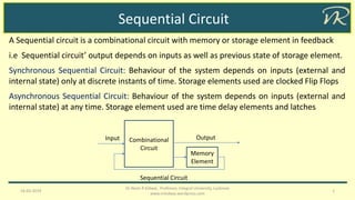
- 1. Sequential Circuit 16-03-2019 1 Dr Naim R Kidwai, Professor, Integral University, Lucknow www.nrkidwai.wordpress.com A Sequential circuit is a combinational circuit with memory or storage element in feedback i.e Sequential circuit’ output depends on inputs as well as previous state of storage element. Synchronous Sequential Circuit: Behaviour of the system depends on inputs (external and internal state) only at discrete instants of time. Storage elements used are clocked Flip Flops Asynchronous Sequential Circuit: Behaviour of the system depends on inputs (external and internal state) at any time. Storage element used are time delay elements and latches Combinational Circuit Memory Element Input Output Sequential Circuit
- 2. Latch 16-03-2019 2 Dr Naim R Kidwai, Professor, Integral University, Lucknow www.nrkidwai.wordpress.com R S Q Q SR Latch using NOR gate Full State table of SR FF S R Qn+1 S R Qn Qn+1 0 0 Qn No Change 0 0 0 0 0 0 1 1 0 1 0 Reset 0 1 0 0 0 1 1 0 1 0 1 Set 1 0 0 1 1 0 1 1 1 1 Invalid 1 1 0 invalid 1 1 1 invalid •Latch holds 1 bit of information •Two outputs are complementary •Inputs are S and R which Sets ( output 1) and Resets (output 0) the latch • S=R=1 is invalid in which rule of complementary output breaks
- 3. SR Flip Flop 16-03-2019 3 Dr Naim R Kidwai, Professor, Integral University, Lucknow www.nrkidwai.wordpress.com Full State table of SR FF S R Qn+1 S R Qn Qn+1 0 0 Qn No Change 0 0 0 0 0 0 1 1 0 1 0 Reset 0 1 0 0 0 1 1 0 1 0 1 Set 1 0 0 1 1 0 1 1 1 1 Invalid 1 1 0 invalid 1 1 1 invalid •In Latch, spurious inputs can cause output change at time. •A clock pulse (in AND to inputs) ensures that inputs are applied only when clock pulse is present R S Q Q SR FF CLK R S CLK Q Q SR Flip Flop symbol 1and; )7,6(5,4,1),,( 1 1 SRQRQSQ QKJQ nn nn SR Characteristics equation
- 4. JK Flip Flop 16-03-2019 4 Dr Naim R Kidwai, Professor, Integral University, Lucknow www.nrkidwai.wordpress.com •JK is modification of SR FF for invalid input combination •For J=K=1, output Toggles (complements) K J CLK Q Q JK Flip Flop symbol R S CLK Q Q J K nQ nQ nnn nn QKQJQ QKJQ 1 1 6,5,4,1),,( JK Characteristics equation Full State table of JK FF J K Qn+1 J K Qn Qn+1 0 0 No Change 0 0 0 0 0 0 1 1 0 1 0 Reset 0 1 0 0 0 1 1 0 1 0 1 Set 1 0 0 1 1 0 1 1 1 1 Toggle 1 1 0 1 1 1 1 0
- 5. Full State table of T FF T Qn+1 T Qn Qn+1 0 No Change 0 0 0 0 1 1 1 Toggle 1 0 1 1 1 0 T Flip Flop 16-03-2019 5 Dr Naim R Kidwai, Professor, Integral University, Lucknow www.nrkidwai.wordpress.com •T FF is JK FF with J=K •For T=1, output Toggles (complements) T CLK Q Q T Flip Flop symbol nQ nQ nnnn nn QTQTQTQ QTQ 1 1 2,1),( T Characteristics equation K J CLK Q Q T
- 6. Full State table of T FF D Qn+1 D Qn Qn+1 0 0 Reset 0 0 0 0 1 0 1 1 Set 1 0 1 1 1 1 D Flip Flop 16-03-2019 6 Dr Naim R Kidwai, Professor, Integral University, Lucknow www.nrkidwai.wordpress.com •D FF is JK FF with J=D and applying NOT gate between J and K •Output is same as Data input (D) D CLK Q Q D Flip Flop symbol DQ QDQ n nn 1 1 3,2),( D Characteristics equation K J CLK Q Q T
- 7. JK Flip Flop: Race around condition 16-03-2019 7 Dr Naim R Kidwai, Professor, Integral University, Lucknow www.nrkidwai.wordpress.com •when J=K=1, output toggles recursively during active period of clock pulse •This leads to unpredictable output state after active period of clock pulse • This condition is know as race around condition K J CLK Q Q JK Flip Flop symbol CLK J K Q •Solution to race around condition • Master slave FF: that gives a single trigger at slave output. How ever race around condition occurs in Master. •Edge triggered FF: flip-flop triggers the ‘edge’ of clock pulse
- 8. Edge Triggered Flip Flop 16-03-2019 8 Dr Naim R Kidwai, Professor, Integral University, Lucknow www.nrkidwai.wordpress.com •Edge triggered FF considers input values at the edge of the clock pulse (either positive or negative) K J CLK Q Q Positive Edge triggered JK FF K J CLK Q Q Negative Edge triggered JK FF CLK J K Q •Timing diagram of typical positive edge triggered JK FF
- 9. Edge Trigger Circuit 16-03-2019 9 Dr Naim R Kidwai, Professor, Integral University, Lucknow www.nrkidwai.wordpress.com •Edge triggered FF considers input values at the edge of the clock pulse (either positive or negative) •Circuit generates a pulse train of pulse duration equal to delay time of invert gate (comparable to rise time or edge duration of clock pulse) • Narrow pulse duration allows only one input trigger in clock pulse CLK y z CLK y z Positive edge pulse train generation circuit
- 10. Conversion of Flip-flops 16-03-2019 10 Dr Naim R Kidwai, Professor, Integral University, Lucknow www.nrkidwai.wordpress.com T→JK FF conversion • Requires design of additional combination circuit (as shown in figure) T CLK Q Q T FF to JK FF Conversion Additional Combinational circuit J K Step 1: Write the desired state table (JK State table) Step 2: Determine what should be value at available FF input for desired state changes (what should be at T to cause Qn→ Qn+1 using excitation table of T Step 3: Write output of additional circuit (T) in SOP and minimize using K map Step 4: Implement the function
- 11. Conversion of Flip-flops 16-03-2019 11 Dr Naim R Kidwai, Professor, Integral University, Lucknow www.nrkidwai.wordpress.com T→JK FF conversion J K Qn Qn+1 T 0 0 0 0 0 0 0 1 1 0 0 1 0 0 0 0 1 1 0 1 1 0 0 1 1 1 0 1 1 0 1 1 0 1 1 1 1 1 0 1 T FF excitation table Qn Qn+1 T 0 0 0 0 1 1 1 0 1 1 1 0KQ QKJT n nQJT mapKusingSolving )7,6,4,3(),,( T CLK Q Q T FF to JK FF Conversion J K