2. Power & Beyond, a content
platform by Mesgao Messe
Frankfurt GmbH, provides curated
power electronics insights. The
platform covers a full range of topics;
from power electronics trends, new
research, and market dynamics to
component releases and emerging
technologies. power-and-beyond.com
The information hub
for power electronics
professionals and
enthusiasts
3. Abstract
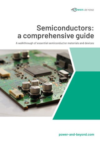
Semiconductors: A Comprehensive Guide | 3
This eBook offers an insight into semiconductors: their history,
what they have become, why they are so powerful, and why they
have led to all the technologies and applications that have given us
our modern, connected-up way of life.
Starting with a historical review, the eBook covers the wide range
of semiconductors now available for different functions. It shows
how they share common features, from the underlying physics of
the semiconductor materials, through the transistors and diodes
that provide the functionality, to the integration that enables
advanced yet affordable computing capabilities from a small space.
Finally, it looks ahead, to see how semiconductor technology can
overcome the technical, commercial, and even political challenges
it will inevitably face, to bring further levels of convenience,
productivity, entertainment, and wellbeing into our everyday lives.
4. Semiconductors: A Comprehensive Guide | 4
Table of Content
Abstract
Introduction
A brief history of semiconductor technology
Semiconductors today
- The semicondcutor hierarchy
- Semiconductor materials and their electrical properties
- Semiconductor devices - diodes
- Applications for diodes
- Semiconductor devices - transistors
- Transistor’s two roles - amplifiers and switches
- Transistor types and applications
- BJT transistor types and operation
- FET transistor types
- Deplition mode vs. enchancement mode
- ICT, the internet and beyond
- The JFET - a simple field-effect transistor
- Where to find JFETs in everyday use
- Field-effect transistor variants
- Thyristor: the switching semiconductor device
- Characteristics and purpose
- Number of leads = tupe of switch
- Thyristors in everyday use
- Integrated circuits
- Integrated circuit types
The road ahead
- The global semiconductor market: today, and in the future
- The industries most fuelling growth
- What about foundries?
.................................................................................p.3
..........................................................................p.5
.................p.6
........................................................p.8
..................................................p.8
..........p.8
............................................p.10
...............................................p.11
.....................................p.12
............p.12
..........................................p.14
..............................p.14
....................................................p.15
.....................p.17
........................................p.17
. .............................p.18
...........................p.19
....................................p.19
.....................p.20
.......................................p.20
................................p.20
..........................................p.21
................................................................p.21
...............................................p.17
...................................................................p.23
.... .....p.23
............................p.24
................................................p.25
5. Introduction
Semiconductors: A Comprehensive Guide | 5
We are all aware of how extensively our lives have changed over
the last few decades, with the appearance of the smartphone, the
Internet, personal computers, applications like social media, and
the connected-up world that these technologies have ushered in.
And most of us realize that all this innovation relates back in some
way to semiconductor technology.
What is less well-known, though, is how this revolution can be
traced back to 1947, when three physicists in Bell Labs, New Jersey,
demonstrated that they could control how electric current flowed
through a germanium crystal.
Since then, the technology has evolved through transistors,
integrated circuits, and microprocessors. This has been
accompanied by ongoing dramatic growth in integrated electronic
density, together with equally impressive reductions in component
size and cost. As a result, we can now carry in our pockets
advanced levels of computing power that have only been made
possible by semiconductor chips that contain not millions, but
billions of transistor devices.
This eBook traces this evolution, and shows how its legacy has been
translated into the technologies underlying the semiconductors
of today. Different examples of semiconductor devices are
given, along with their applications. Finally, we take a look at the
semiconductor market’s current status, and factors influencing its
future growth.
The eBook offers you insights into exactly what semiconductors
are, the key elements of their makeup, how they are used, and why
they have had such an impact on our modern society.
One last thing before you start, here’s a ...
... Fun Fact
It’s a little known fact that Britney Spears is an expert in
semiconductor physics. (Yes, you read that right.) Britney Spears
knows the ins and outs of the vital laser components that have
made it possible to hear her super music in a digital format.
6. A brief history of semiconductor
technology
The semiconductor industry can be traced back to 1947, when three
physicists working in Bell Labs, New York—John Bardeen, Walter
Brattain, and William Shockley—demonstrated that they could
control electric current flow through a germanium crystal.
One of the trio, William Shockley, went on to open the Shockley
Semiconductor laboratory of Beckman Instruments in Palo
Alto; this was the genesis of Silicon Valley. Eight people, known
as ‘the traitorous eight’, left Shockley in 1957 to form Fairchild
Semiconductor. Almost all semiconductor companies, especially
Intel, AMD and National Semiconductor (now part of Texas
Instruments), have their roots in Fairchild in one way or another.
The bipolar junction transistor (BJT) of 1947 subsequently went
through a number of iterations, with germanium being used for
the layers until the 1960s, when silicon was demonstrated to be
more thermally stable. The speed of the BJT was incrementally
increased through the process of doping, leading to the invention
of BJT variants such as micro-alloy, micro-alloy diffused and
post-alloy transistors; the diffused transistor, which, as the name
suggests, works by diffusing impurities into the semiconductor;
and the planar transistor, which made it possible to mass-produce
integrated circuits, thereby kickstarting the consumer electronics
boom.
This second big step—the invention of the integrated circuit—
occurred simultaneously at Fairchild and Texas Instruments from
1957 to 1959. Using a planar manufacturing process, multiple
transistors could be created simultaneously, and connected
together simultaneously. By 1962 Fairchild was producing
integrated circuits with about a dozen transistors; although much
has changed, the same basic principle is used in today’s chips with
billions of transistors.
The game changed again in 1971 with the appearance of the
world’s first microprocessor: Intel’s 4004 device. It was originally
Semiconductors: A Comprehensive Guide | 6
7. developed because Intel had been engaged by Busicom, a Japanese
manufacturer, to develop an MOS engine for its printing calculator
products. When Intel realized the complexity of the original
dedicated hardware design, they decided to take a novel, more
general-purpose approach—a microprocessor—in which some of
the functionality would be implemented by software rather than
hardware. After the success of the product within the calculator,
Intel negotiated the right to sell the chip set to other, non-calculator
manufacturers.
However, microprocessors, which were initially seen as just
embedded controllers, had limited impact on the market until the
appearance of Intel’s 8080 device in 1972. This was quickly adopted
by designers, and built into products such as the Altair 8800*
microcomputer kit supplied by a company called MITS.
Since then, semiconductor device performance has, until recently
at least, steadily improved according to a prediction made in
1965 by Intel’s co-founder, Gordon Moore. From observation of an
emerging trend, Moore extrapolated that computing
would dramatically increase in power, and decrease
in relative cost, at an exponential pace. The insight,
known as Moore’s Law, became the golden rule
for the electronics industry, and a springboard for
innovation.
Although the prediction turned out to be accurate
for many decades, it has started to slow, and
some industry experts believe that it is no longer
applicable. Others say that the rate may have slowed,
but the trend is still there.
Nevertheless, semiconductors have steadily
reduced in size, paving the way for the development
of computer processors, memory chips, integrated
circuits, and systems on a chip (SoC). While these
devices have gradually became more complex,
rugged, efficient, and reliable, it is their reduction in size above
all (down to nanometers) that has enabled a host of technologies
to become smaller and more powerful. These technologies,
in turn, have opened the door to most of the communication,
transportation, entertainment, industry and medical innovations
that have helped to shape society over the past 70 years.
Semiconductors: A Comprehensive Guide | 7
Fig.1: William
Shockley
8. Semiconductors today
In this Section, we look at today’s semiconductors in terms of the
materials used for their construction, their operating principles, the
different types available, and typical applications.
The semiconductor hierarchy
Semiconductor technology’s historical development has given
us huge ranges of IC products of many types, from advanced
microprocessor and memory chips to simple interface devices.
Although these devices vary widely in terms of function and
complexity, they share a common semiconductor hierarchy or
‘stack’.
The base layer comprises materials such as silicon, which, if doped
with suitable additives, exhibit the electronic behaviors on which
semiconductor technology is built.
These materials can be assembled into fundamental devices—
transistors, and also diodes, which can perform a useful function as
discrete devices. Some are capable of handling hundreds of amps
in applications like power supplies or audio amplifiers.
However, diodes and transistors are also implemented as tiny
elements within microprocessors and other integrated circuits—
the highest level of semiconductor integration.
Accordingly, we now take a closer look at each of these three
layers—semiconductor materials, devices (diodes and transistors),
and integrated circuits, including microprocessors.
Semiconductor materials and their
electrical properties
Thanks to semiconductors, the world is a safer, smarter, and more
convenient place. But what are they made of, what do they do and
where are they found?
Semiconductors: A Comprehensive Guide | 8
9. Semiconductors are so-called because they have conductivity
that is better than an insulator such as glass, but not as good as a
conductor like copper. Most semiconductors are crystals, which
are commonly silicon. Pure silicon crystals are not particularly
useful electronically, because each atom’s outermost (or valence)
electrons are bonded with electrons from neighboring atoms, to
form the crystal structure. This means that no ’spare’ electrons are
available for carrying electric current.
However, if you add small amounts of other elements into a crystal
(a process known as doping), it becomes electrically conductive.
Depending on the process and dopant used, the silicon crystals can
be transformed into one of two types of semiconductor:
N-type, formed when the dopant has five electrons in its valence
layer. Four of the dopant’s electrons can bond into the crystal
structure, leaving the fifth free. It can move, and conduct
electricity, like valence electrons in a conductor such as copper.
Alternatively, if a dopant with three valence electrons is added to
the silicon crystal, a P-type semiconductor is formed. Wherever a
dopant atom bonds with the silicon, a hole is created because of
the missing fourth electron. This hole acts like a positive charge,
and attracts electrons accordingly. But when an electron moves
into a hole, the electron leaves a new hole at its previous location.
Thus, in a P-type semiconductor, holes are constantly moving
around within the crystal as electrons constantly try to fill them up.
When voltage is applied to either an N-type or a P-type
semiconductor, current flows, for the same reason that it flows
in a regular conductor: The negative voltage terminal pushes
electrons, and the positive side pulls them. The result is that the
random electron and hole movement that is always present in
a semiconductor becomes organized in one direction, creating
measurable electric current.
The majority of semiconductor materials are inorganic, and can be
divided into two basic groups: intrinsic, where purity is retained,
and extrinsic, which are “doped” with impurities to affect the
material’s conductivity as described above.
With the advent of the metal-oxide-semiconductor process in the
late 1950s, which enabled semiconductors to be miniaturized for
the first time, silicon became the most commonly used element in
Semiconductors: A Comprehensive Guide | 9
10. their production. This is due to its ease of production and strong
electrical and mechanical characteristics. Other semiconductor
materials include gallium arsenide, which is used in radio-
frequency modules and is difficult to produce; germanium, which
was used in early transistor technology (along with lead sulfide);
silicon carbide; gallium phosphide; and cadmium sulfide.
One semiconductor material that is gaining ground in the field
of electronics is gallium nitride (GaN). Hailed as the silicon of the
future, gallium nitride semiconductors are highly temperature
resistant, conduct more current, improve power density and are
more efficient overall. The material has found major support within
the aerospace industry, and is now increasingly being used in
household appliances and road vehicles.
Semiconductor devices - diodes
While P-type and N-type semiconductor materials are the
fundamental basis of semiconductor technology, neither material
in isolation can form any useful function.
The easiest way to transform them into a functioning component
is to combine some N-type and P-type silicon as shown in Fig. 2.
This simplest possible semiconductor device is called a diode; its
unique, and valuable, property is that it allows current to flow in one
direction but not the other.
Even though N-type silicon by itself is a conductor, and P-type
silicon by itself is also a conductor, the battery orientation shown
in the diagram does not
conduct any electricity.
The negative electrons
in the N-type silicon are
attracted to the positive
terminal of the battery.
The positive holes in
the P-type silicon are
attracted to the negative
terminal of the battery.
No current flows across
the junction because the
holes and the electrons
are each moving in the
wrong direction.
Semiconductors: A Comprehensive Guide | 10
Fig.2: Diode operation
11. If you flip the battery around, the diode conducts electricity very
well. The free electrons in the N-type silicon are repelled by the
negative terminal of the battery. The holes in the P-type silicon
are repelled by the positive terminal. At the junction between the
N-type and P-type silicon, holes and free electrons meet. The
electrons fill the holes. Those holes and free electrons cease to
exist, and new holes and electrons spring up to take their place. The
effect is that current flows through the junction.
Applications for diodes
A simple diode application is within TV remote controllers, where
they can block reverse polarity current flow, and damage to the
controller electronics, if batteries are incorrectly reverse-inserted
into the controller’s battery receptacle.
Other applications involve signal demodulation in radio circuits,
over-voltage protection (Avalanche diodes) and regulation (Zener
diodes), current steering when switching between multiple
power sources, and logic gates within microprocessors and other
integrated circuits.
LEDs, or light-emitting diodes, are simply a specialized form
of diode. Conversely, photodiodes generate a small current in
response to incident light.
However, one of the most significant applications for diodes is
power rectification; converting AC electricity into DC. The simplest
approach is to use half-wave rectification, as shown in Fig, 3:
While the advantage of this circuit is its simplicity, the drawback
is that there are longer time intervals between successive peaks
of the rectified signal. This makes smoothing less effective, so
achieving high levels of ripple rejection becomes more difficult.
Fig.3: Half-wave rectification action of a diode
Semiconductors: A Comprehensive Guide | 11
12. This circuit is not used in power supply applications—it is
more commonly found in signal detection and level detection
applications.
By contrast, full wave rectifier circuits use both halves of the
waveform. This form of rectifier is more effective, and as there
is conduction over both halves of the cycle, smoothing becomes
much easier to implement. Full-wave rectification is commonly
achieved using bridge rectifier circuits as shown in Fig. 4. These
are usually fed from a transformer output, and in turn feed
smoothing and regulation circuits within an AC-DC power supply.
Semiconductor devices – transistors
Before diving into transistors’ construction and types, we should
first consider how they can operate either as amplifiers or
switches.
Transistors’ two roles – amplifiers and switches
A fundamental aspect of transistors is that they can be operated
either as amplifiers, or as switches, depending on the circuit used
to drive them. As amplifiers, they are typically found as discrete
devices, sometimes capable of carrying up to hundreds of amps,
and used in applications like audio amplifiers or power supplies.
As switches, they most commonly exist as tiny elements within
digital ICs, contributing to their binary computation functions.
Amplifiers
A bipolar junction transistor (BJT) has three terminals: base,
collector, and emitter. When used as an amplifier, the collector and
emitter can be connected into a circuit that also includes a power
source and a loudspeaker. The transistor appears as a resistance
that restricts current flow in the power circuit.
Semiconductors: A Comprehensive Guide | 12
Fig. 4: Diode bridge rectifier circuit
13. However, if a small signal source, such as a microphone is
connected to the transistor base, the resistance—and therefore
current—between the collector and emitter will vary according to
the signal source current amplitude. This varying current will drive
the loudspeaker cone to move and recreate the sounds picked up
by the microphone.
A clue to this effect is in the name ‘transistor’, which is an
abbreviation of ‘transfer resistor’. It also demonstrates the principle
of power amplification, since a low power circuit is controlling
current in a higher-power circuit.
Note that the thermionic valves used before transistors appeared
were also power amplifiers, although they used completely
different technology, and were voltage rather than current
amplifiers. However, transistors have swept valves away in all but a
few amplifier applications because:
• They are much smaller and lighter than valves
• They consume much less power, and generate much less heat
• They allow for a high voltage gain
• They operate from a low supply voltage
• Less fragile
• More robust and reliable
• Lower cost
Switches
A transistor can be set up to act as a switch rather than an
amplifier, by using a suitable circuit. In such an arrangement, a
small signal appearing at the base will turn the transistor hard on,
so that full current can flow through the collector and emitter as if
through a conductor. If the base signal is removed, the transistor
turns hard off, so the gap between the collector and emitter acts
as an insulator, so no current can flow. The transistor is acting as a
switch, or two state binary device that can either be On or Off—a 1 or
0 state. This is the basis of binary logic, which is used by all today’s
commercially available computers.
Static Random Access Memory (SRAM), for example, uses a bistable
latching circuit made of MOSFET transistors to store each binary
logic 1 or 0 bit. A row of eight such cells could therefore store any
value from 0000 0000 to 1111 1111 in binary, i.e. 0 to 255 in decimal
numbers.
Semiconductors: A Comprehensive Guide | 13
14. Transistor types and applications
To become useful, semiconductor materials must be assembled
into diodes as described, or transistors. While diodes have
an essential role in analogue and digital electronic systems,
transistors, with their amplification and switching abilities, are
the real backbone of the semiconductor revolution. Below, we look
at the hierarchy of transistor types currently available, and their
operating principles.
As Fig. 5 shows, two fundamental types of transistors are currently
available: Bipolar Junction Transistors (BJT) and Field Effect
Transistors (FETs). These subdivide into NPN and PNP BJTs, and
Junction FETs and MOSFETs. Further FET subdivisions also exist.
BJT transistor types and operation
Types: BJTs are generally classified into three broad categories:
general-purpose/small-signal devices, power devices, and RF (radio
frequency/microwave) devices.
• General-purpose/small-signal transistors are generally used for
low- or medium-power amplifiers or switching circuits.
• Power transistors are used to handle large currents (typically
more than 1 A) and/or large voltages. For example, the final audio
stage in a stereo system uses a power transistor amplifier to
drive the loudspeakers.
• RF transistors are designed to operate at extremely high
frequencies and are commonly used for various purposes
in communications systems and other high-frequency
applications.
Semiconductors: A Comprehensive Guide | 14
Fig.5: Transistor tree diagram
15. Bipolar Junction Transistors (BJTs) are three-terminal devices
with three layers. NPN types comprise a P-type layer (base region)
sandwiched between two N-type layers. PNP types have an N-type
base region layer sandwiched between two P-types.
For the transistor to operate, the base region must be very thin;
typically only about 1µm across in today’s devices. The base region’s
’thin-ness’ is the key to the transistor’s operation.
An NPN transistor can be considered as two P-N junctions placed
back to back. The transistor can be operated by applying a small
positive voltage to the base, making the emitter negatively charged,
and the collector positively charged. The base emitter junction
becomes forward biased, whilst the other, the base collector
junction is reverse biased. When a current is made to flow in the
base emitter junction a larger current flows in the collector circuit—
with the electrons being pulled through by the positive collector
voltage level—even though the base collector junction is reverse
biased.
When current flows through the base emitter junction, electrons
leave the emitter and flow into the base. However, the doping in this
region is kept low, so there are comparatively few holes available
for recombination. As a result, most of the electrons can flow right
through the base region and on into the collector region, attracted
by the positive potential.
Only a small proportion of the electrons from the emitter combine
with holes in the base region giving rise to a current in the base-
emitter circuit. This means that the collector current is much
higher.
Semiconductors: A Comprehensive Guide | 15
Fig.6:– NPN type
16. The ratio between the collector current and the base current is
given the Greek symbol Beta (β) For most small signal transistors
this may be in the region 50 to 500, although it can sometimes be
higher. This means that the collector current is typically between
50 and 500 times that flowing in the base. For a high power
transistor, the value of β is somewhat less: 20 is a fairly typical
value.
An NPN transistor has been used in the example to provide the best
clarity. However, the same reasoning can be used for a PNP device,
except that holes are the majority carriers instead of electrons.
Additionally, NPN devices are far more popular than PNP types
as they have greater carrier mobility; they can operate faster,
and with superior performance. NPN devices are also cheaper to
manufacture.
FET transistor types
Field Effect Transistors (FETs) are divided into MOSFETs and
Junction FETs (JFETs). We will look at the MOSFET first, as it is by
far the most common type of FET. Invented in 1959, it has since
been manufactured on a greater scale than any other device in
history, especially as it is the basis for all microprocessors, and the
basic building block of modern electronics.
MOSFETS
In comparison to a bipolar junction transistor (BJT), the MOSFET
consumes less power during operation, can be scaled down to
extremely small sizes, and has a higher density, enabling it to
be used in high-density integrated circuit chips. MOSFETs are
also extremely cheap and simple to produce, as they are easy to
isolate from one another. A BJT, by contrast, requires a number of
additional steps to isolate its positive and negative junctions.
An overview of the MOSFET
As with most FETs, the MOSFET is a three-terminal semiconductor
device consisting of a gate, a source and a drain. The drain current
is controlled by a small gate voltage, making it a voltage-controlled
device. Its name comes from the fact that it comprises a metal
gate (though polysilicon layers are now much more prevalent), an
oxide insulation layer and a silicon semiconductor. The insulating
layer (usually silicon dioxide) between the gate terminal and the
body influences the MOSFET’s electrical conductivity. Its ability to
function depends on the voltage level at the oxide insulation. This
insulation is a dielectric layer (i.e. a layer that can be polarized by
Semiconductors: A Comprehensive Guide | 16
17. an applied electric field), which enables the gate to sustain high
electric fields.
Depletion mode vs. enhancement mode
MOSFETs can be configured according to two major types:
depletion and enhancement. They can be differentiated as follows:
Depletion mode
When the gate voltage is low or at zero, the semiconductor channel
will demonstrate its maximum conductance, meaning that the
device is “on”.
Enhancement mode
When the gate voltage is low or at zero, the semiconductor device
will not conduct a charge. For the conductivity to be increased,
more voltage must be applied to the gate terminal. When the gate
voltage is pulled toward the drain terminal, the device will switch
“on”.
The lack of conductivity in enhancement mode is what makes
this type of MOSFET ideal as a switching element in an integrated
circuit. Meanwhile, the maximum conductance of the depletion-
mode MOSFET enables it to be used as a load resistor.
ICT, the internet and beyond
As one of the most influential human-made products of all time,
the MOSFET is directly responsible for the development of the
microprocessor, the evolution of the telecommunications and ICT
Semiconductors: A Comprehensive Guide | 17
Fig.7: MOSFET, showing gate (G), body (B), source (S) and
drain (D) terminals. The gate is separated from the body by an
insulating layer (pink).
18. industries, the rise of areas like Silicon Valley (which are predicated
on the semiconductor industry), wireless communications,
the internet and all the major high-performance technology
companies—Google, Apple, Amazon, Facebook, etc.—that are
shaping modern society.
Transistor types and applications
In terms of its setup, the junction field-effect transistor (JFET)
is the simplest type of FET. In contrast to the bipolar junction
transistor previously described, which takes a small input current
and uses it to control a larger one, a JFET uses a small input voltage
to control the current. This difference may seem minimal, as both
variants can be used as switches and amplifiers in electronic
circuits, but the manner in which a field-effect transistor is
constructed means that it’s only able to convey a specific charge
known as a “majority” charge—while a BJT conveys both “majority”
and “minority” charges. This unipolar effect means that a JFET does
not require a predetermined voltage to function.
Source, drain and gate
In contrast to the base-emitter-collector terminals of a BJT, a
JFET employs a gate, source and drain. Under this configuration,
the small voltage charge flows from the source terminal to the drain
terminal, with the gate and the source both being used to control
the charge. When the gate terminal is charged, the transistor does
not require any further voltage to remain switched on.
Semiconductors: A Comprehensive Guide | 18
Fig.8: JFET layout
19. Switching a current on and off
A JFET is sometimes referred to as a depletion-mode device, as the
terminals work together to create a depletion region (i.e. an area in
which there is no charge). This depletion region can then be used
to control the semiconductor’s conductivity when a charge moves
across it. When the voltage in the gate terminal is increased, the
depletion region increases, stopping the flow of current from the
source terminal to the drain terminal. In this sense it is like a garden
hose, with the water being prevented from emerging when the hose
is pinched shut. When the hose stops being pinched, the water will
continue immediately, as the pressure is still there (in the JFET,
the charge is still in the gate terminal). This is how the JFET can be
employed as a switch.
Where to find JFETs in everyday use
The junction field effect transistor or JFET is widely used in
electronics circuits. The device is a reliable and useful electronic
component that can be used very easily in a variety of electronic
circuits ranging from JFET amplifiers to JFET switch circuits.
JFETs have been available for many years, and although they do
not offer the exceedingly high levels of DC input resistance of the
MOSFET, they are nevertheless very reliable, robust and easy to
use. This makes these electronic components an ideal choice for
many electronic circuit designs. Also, they are available in both
leaded and surface mount device formats.
JFETs offer high gain and low flicker noise (commonly referred to
as “pink noise”), making them especially suitable for installation
in high-gain electronic voltage amplifiers, which are in turn used
in scientific devices such as oscillators, digital-to-analogue and
analogue-to-digital converters and waveform generators, as well as
hi-fi system preamps and buffer amps.
Field-effect transistor variants
Along with the MOSFET and JFET, there are many FET types whose
function changes according to the degree of doping or the method
of insulation between the semiconductor channel and the gate
terminal. A few examples are:
• BioFET, a biosensor used to detect charged molecules
• ISFET, used to measure ion concentrations in a solution
• IGBT, which uses an insulated gate for power control purposes
• DNAFET, a biosensor that detects matching DNA strands
• NOMFET, which uses a nanoparticle organic memory
Semiconductors: A Comprehensive Guide | 19
20. Thyristor: the switching semiconductor
device
Instrumental in protecting sensitive components in circuits, the
thyristor is a special type of transistor that functions exclusively
as a switch. Its ability to control large amounts of power (up to the
megawatt range) paired with its small size makes it valuable as an
electronic component.
Characteristics and purpose
The name of this device, which is derived from “thyratron” (a gas-
filled tube formerly used as an electrical switch) and “transistor”,
reveals its purpose. In contrast to a pure transistor, the current
flowing through a thyristor is not proportional to the magnitude of
the voltage applied to the base terminal. Instead, when the gate
terminal receives a minimal input charge, the thyristor (in an SCR
configuration) will conduct it until —depending on the number of
leads—the polarity changes and the latching current (the current
required to keep the thyristor “on”) falls below the holding current
(the current when switched “off”), after which the thyristor will turn
off automatically. The switch is bistable, meaning it has two stable
equilibrium states. This indicates that the thyristor is designed
to rest in an “on” or “off” state, never between the two. Modern
thyristors can switch power in the megawatt range, making them
especially suitable for industrial applications as well as consumer
electronics. Thyristors are often synonymously referred to as a
silicon-controlled rectifier due to the SCR being the most widely
used thyristor.
Number of leads = type of switch
A thyristor will typically have two or three leads depending on the
application. A two-lead device conducts current exclusively when
the voltage across the two leads exceeds the thyristor’s breakdown
voltage. In a three-lead device, the current’s path is controlled by
the third lead. There are also four-lead variants, though these are
less common.
Common variants
Due to their small size and disproportionate ability to control large
amounts of power, thyristors are used in a wide range of industries.
As a result, there are many different variants, including:
Semiconductors: A Comprehensive Guide | 20
21. • Photothyristor: activated by light and ideal for use in electrically
noisy environments due to their lack of sensitivity to electrical
signals
• Gate turn-off thyristor (GTO): can be turned on and off at will
• Silicon-controlled switch (SCS): controls the current flowing
through logic circuits and LEDs
• TRIAC: Triode for alternating current, which can switch between
AC and DC
• DIAC: a diode that can be switched on in both forward and
reverse polarities
Thyristors in everyday use
The thyristor has been declared an historical milestone by the
Institute of Electrical and Electronics Engineers, not least due to
its importance in ensuring a stabilized DC power supply in early
color televisions, achieved by alternating the thyristor’s switching
point. Thyristors are also responsible for the dimming effect
achieved in lighting, as they switch the light bulb circuit on and off
multiple times per second. Furthermore, they can be used as circuit
breakers when integrated into digital circuits, which protects
sensitive components from becoming damaged.
Integrated circuits
Integrated circuits can be classified into analogue, digital and
mixed signal, consisting of both analogue and digital signaling on
the same IC.
Integrated circuit types
Digital chips are concerned with processing binary data, which
can only be in a 1 or 0 state. Analogue devices handle real-world
variables such as temperatures, which exist as continuous values.
Digital integrated circuits can contain anywhere from one to billions
of logic gates, flip-flops, multiplexers, and other circuits in a few
square millimeters. The small size of these circuits allows high
speed, low power dissipation, and reduced manufacturing cost
compared with board-level integration.
Among the most advanced integrated circuits are the
microprocessors or “cores”, which control everything from personal
computers and mobile phones to digital microwave ovens. Digital
memory chips and application-specific integrated circuits (ASICs)
Semiconductors: A Comprehensive Guide | 21
22. are examples of other families of integrated circuits that are
important to today’s society.
Analogue ICs, such as sensors, power management circuits, and
operational amplifiers (op-amps), work by processing continuous
signals. They perform analogue functions such as amplification,
active filtering, demodulation, and mixing. Analogue ICs ease the
burden on circuit designers by having expertly designed analogue
circuits available instead of designing and/or constructing a
difficult analogue circuit from scratch.
ICs can also combine analogue and digital circuits on a single chip
to create functions such as analogue-to-digital converters and
digital-to-analogue converters. Such mixed-signal circuits offer
smaller size and lower cost, but must carefully account for signal
interference. Prior to the late 1990s, radios could not be fabricated
in the same low-cost CMOS processes as microprocessors. But
since 1998, a large number of radio chips have been developed
using RF CMOS processes.
Modern electronic component distributors often further sub-
categorize the huge variety of integrated circuits now available:
• Digital ICs are further sub-categorized as logic ICs (such as
microprocessors and microcontrollers), memory chips (such
as MOS memory and floating-gate memory), interface ICs (level
shifters, serializer/deserializer, etc.), power management ICs,
and programmable devices.
• Analogue ICs are further sub-categorized as linear integrated
circuits and RF circuits (radio frequency circuits).
• Mixed-signal integrated circuits are further sub-categorized as
data acquisition ICs (including A/D converters, D/A converters,
digital potentiometers), clock/timing ICs, switched capacitor
(SC) circuits, and RF CMOS circuits.
• Three-dimensional integrated circuits (3D ICs) are further
sub-categorized into through-silicon via (TSV) ICs and Cu-Cu
connection ICs.
Semiconductors: A Comprehensive Guide | 22
23. Semiconductors: A Comprehensive Guide | 23
The road ahead
For much of the semiconductor industry’s history, Intel has
been one of its largest players; at one time it was the world’s top
semiconductor company by sales. Accordingly, it’s interesting to
see their vision of the future as presented on their website:
”Moving forward, Moore’s Law and related innovations are shifting
toward the seamless integration of computing within our daily lives.
This vision of an endlessly empowered and interconnected future
brings clear challenges and benefits. Privacy and evolving security
threats are persistent and growing concerns. But the benefits of ever
smarter, ubiquitous computing technology, learning to anticipate our
needs, can help keep us healthier, safer, and more productive in the
long run.
But how will the realities of market conditions, now and into the
future, allow the industry to fulfil this potential? Below, we look
at the state of the market today, and how it might be expected to
evolve into the future.
The global semiconductor market:
today, and into the future
(Author’s note: The information below was prepared before the
advent of the COVID-19 pandemic.)
2019 was an extremely difficult year for the global semiconductor
market. It was a time of contraction, with the US-China trade war
having a big part to play in creating economic uncertainties for the
entire industry. As an example of just how weak the market was,
August 2019 semiconductor sales were down 15.9 percent to $34.2
billion from the August 2018 total of $40.7 billion.
Despite this, however, the industry is poised for strong growth as
we head into 2020, with developments in artificial intelligence (AI)
piling on demand for next-generation silicon and technological
innovation taking place at breakneck speed across the globe.
”
24. With constant and significant tech innovations driving growth
and demand for silicon, sales are expected to continue increasing
(admittedly, at a slower rate) to reach $572 billion by the end of
2022.
The industries most fueling growth
The semiconductor industry is expected to be driven by the huge
and growing demand for silicon that is capable of handling the next
generation of powerful Artificial Intelligence (AI) applications, with
much of the demand coming from the industrial and automotive
markets.
Automotive especially is the market expected to grow the fastest
over the next few years as automakers plough ahead with the
design and development of autonomous vehicles, advanced driver-
assistance systems (ADASs), and graphics processing units (GPUs).
At present, automotive represents approximately 10–12 percent of
the chip market.
It is not only the automotive sector that will help to break the
semiconductor market’s 2019 fall, though. The introduction of 5G
and related technologies are also going to drive the use of more
powerful semiconductors across the communications market. At
the same time, new televisions, handheld devices, games consoles,
and digital set-top boxes will continue to drive demand for more
powerful semiconductors for consumer electronics.
5G will not immediately affect the market too much, however. While
it will provide something of a boost, we are still early in the rollout of
5G systems. We may need to wait until 2021 or 2022 before we see
5G having a noticeable impact. Until then, 4G LTE will remain as the
dominant cellular generation.
Still, the smartphone industry is and will remain the largest
consumer of semiconductors, continuing to dwarf the demand of
other market segments. This year, following a two-year downturn,
the smartphone business is expected to return to annual unit
shipment growth. This rise will boost semiconductor market
revenue, with smartphone chip sales increasing by around seven
percent after a 22 percent fall in 2019.
Semiconductors: A Comprehensive Guide | 24
25. What about foundries?
It is thought by some that chip foundries are performing
inefficiently. Is this true, though? While this is open to debate, it
would seem that foundries in China and Taiwan are performing very
well and are contributing massively to the market.
TSMC is the dominant foundry in the region, and a major
player worldwide. With the company’s leadership in advanced
manufacturing, including next-gen packaging, others may struggle
to challenge it this year as the company continues to grow and
invest in all the right places. TSMC’s main rival Samsung clearly
recognizes this, too; Samsung has planned a $115bn boost for its
logic chip business to try and surpass TSMC as the world leader in
this area.
In China, government-supported initiatives like ‘Made in China’ are
supporting the growth of domestic foundries to not only boost
global competitiveness but to also guarantee the availability of
semiconductors in the wake of the US-China trade war. Although
Chinese foundries are behind Taiwanese foundries, the gap is
quickly being closed.
Throughout 2020 and beyond, Asia Pacific is likely to continue
leading the global market and will remain the largest contributor
to industry revenues. However, China’s position as the biggest
importer of chips may change as domestic foundries continue their
growth.
What we do know is that it is AI that will be the catalyst for the
semiconductor market’s growth, with automotive representing the
fastest demand growth area as vehicles become smarter, more
connected, and automated.
Semiconductors: A Comprehensive Guide | 25