SlideShare a Scribd company logo
1 of 25
Printed Ckt Board
Types of PCB
(I) Single Side (II) Double Side (III) Multi Layer
(V) Flexible PCB
* Single Side ( 1 layer ) :- The insulating substrate contains ckt pattern on
only one side. Which is called as solder side. The other side is called component side.
* Double Side (2 layer) :- Double side means the ckt pattern is present on
the either side of the insulating material ckt pattern both on component side & solder side.
* Flexible Cards :- Flexible boards are similar to rigid boards except
the board are made from a flexible substrate material. The base materials are very thin and
the common thickness is 0.1mm.
* Multi layer Board (MLB, 4L,6L,8L,12L,16L ) :-
The ckt density is high compare to D/S for inner layer
made of special laminate is used for bonding purpose ( Prepreg). The inner layer
is etched “CU” and outer layer is Non- etched ckt. After lamination or pressing
the boards are drilled and plated like PTH D/S.
Process Flow chart for Single Side P.C.B.
Sheet Cutting Film master preparation Screen Preparation
Drying Screen Printing Board cleaning
Retouching Etching Drilling Ink Stripping
Legend Printing Roller Tinning or HAL Masking
Final Cutting Q.C.
Process Flow Chart of Double Side P.C.B.
Sheet Cutting Film Master Preparation CNC Drilling
Photo Printing PTH or Electroplating Board Cleaning
Pattern Plating or Electro Plating Dry film Stripping Etching
H.A.L. Green Masking Tin Stripping
Legend Printing Final Cutting Q.C.
Mechanical Operation
* Sheet Cutting :- Measure the size of PCB from film or
Artwork.
W
L
* Board Area
Panel Sz.
PCB Sz.
Boarder Area
* Laminates or Copper Sheet :-
1. Glass Epoxy 2. Paper fenolic 3.Teflon 4. Ceramick (CEM)
* Glass Epoxy :- Thickness S/S 1.6 35/0 Cu Thickness
Insulating Material
thickness
D/S 0.8-18/18
1.6-18/18
2.4-18/18
3.2-18/18
Base material is reinforced with glass fiber or paper fiber as filler and epoxy resin and the cu
foil is pressured over it to get cu clad laminates.
* Paper Phenolic :- Phenolic laminates are reinforced with paper fillers and the cu foil
is pressed to the base material.
Thickness :- Fr-2, C-8000, 1.6- 35/0------ S/S, 0.8-18/18--- D/S
1.6- 18/18-----D/S
* Teflon Laminates :- Teflon is reinforced with glass fiber to get
aminates of low dielectric constant and it is used in Radio frequency.
* SHEARING MACHINE :- Used for laminate cutting for PCB
production.
* Manual Shearing * Motor drive Shearing.
* Final Cutting i.e. cutting in finish size.
* Shearing Blades :-Two Blades :- (I) Fixed Blades
(ii) Movable Blades.
* Punching :-Making Big hole, slot of different shape Die &Punch.
1 to 1.50
* Blanking :- Clean Cutting operation is done with a punching tool.
* Routing :- Final Cutting by CNC machine or Pin router
* Drilling :- (I) Manual Drilling
(ii) CNC Drilling ( Computer numeric Control)
* Manual Drilling :- * Used H.S.S. Drill Bit
* Speed of M/C is 6,000-16,000 RPM
* Stack Drilling
* Jig Drilling.
CNC Programming & Drilling
(I) Do path making
(II) Focus the Hole with help of camera and monitor.
(III) For time saving and maintained the accuracy.
(IV) After programming Drill one Panel for checking the
program.
(V) Checked Missing Hole, Extra Hole,Shifting, Inter changed Hole, Drill Dia (
Drill dia checked by Hole Gauge. )
T3 T2
T1 Path Making
* Drill Bit :- Tungsten Carbide drill bit used in CNC machine.
Shank dia
* In double side PCB drill dia is always 0.1mm extra from finish size.
3.175
*. Ink Stripping/ Dry film :-
To remove the ink by using Naoh or Koh solution.
Ink remove and the cu appears on track and pads only.
Masking
(I) Thermal Masking (II) PISM ( Photo Imagable solder Mask)
# Thermal Masking :-
*. Using Screen Printing.
*. -ve Masking film used in thermal masking.
*. Ink in paste form added Hardener and
masking reducer for making liquid form.
# P.I.S.M.:-
* Using Photo Printing Method.
* + ve Masking film used in PISM.
* Panel coated with PISM ink.
* Dry in oven or UV Light.
* Panel develop in Na2co3 solution.
# Peel off Test
#. To cover the panel with insulating ink.
#. To protect the cu for oxidation
# To avoid the short ckt.
Brushing (Surface Preparation)
To remove the dust particles and oxide layer from the surface of panel.
.
*. Chemical cleaning *. Mechanical cleaning
* Chemical Cleaning :- Using Alkali chemical to remove oil, grease & soil particle
on the surface of laminates.
* Mechanical Cleaning :-
Laminate Drilling Deburing (320 grid brush)
Water rinse Buffing (wet condition ) Water rinse
Drying (with hot blow air )
FILM MASTER PREPARATION
* High efficiency Compact camera used for reduction and inlargement
purpose.
Material Used :- (I) Lith film
(ii) Lith film Developer
(iii) Sodium Thosulphate
(iv) Developing Trays
(v) Retouching Ink
(vi) Retouching Brush
(vii) Butter Paper
* Art Work :- (I) Manual Artwork (ii) Take Design Print out
* Lith film Developer :- PART- “A”(P-Methyl amino phenol sulphats
PART- “B” ( Sodium Carbonate )
Temp.- 200
+--
30
c
* Fixer :- Sodium Thosulphate
* Retouching :- Using Opaque ink for cover the pin holes.
SCREEN PRINTING
It is done with the help of a wooden/ Aluminum frame having a
polyester cloth tightened over it. Polyester is available in different meshes. Which
are indicated by “T” that indicate the number of thread gapping.
Wooden frame
Three methods for Screen Printing :-
(I) Direct Method :- Ammonium dichromate or Potassium dichromate is
mixed with super coat solution in 1:3 ratio.
(II) Indirect Method :- Using Five Star film.
* Film Develop in H202 (Hydrogen Peroxide Solution )
(III) Direct-Indirect Method :- Chromaline film is used.
* Printing Ink :- Acid Resist Blue ink for Printing of
Single Side PCB.
* Squeegees :- The sharpness of the squeegees is very
important for printing. Line sharpness. Uniform ink
coating thickness and the edge definition depends on
the squeegees sharpness.
ETCHING
(1)Immersion (2) Bubble (3) Splash (4) spray Etching
* Ferric Chloride Etching Solution
Fecl3 350-500 g/ltr
HCL 60 to 65 ml/ltr
Temp 200
c to 300
c
Cu +Fecl3 Fecl2 +Cucl (Green Color )
* Chromic Sulfuric Acid Etchant
Chromic Acid
H2so4
Temp
200 to 240 g/ltr
60 to 65 ml/ltr
20 to 300
c
* Ammonium Chloride Etchant
Ammonium Bicarbonate
Ammonium Nitrate
Cupric Chloride
Ammonium Chloride
Temp
75g/ltr
80g/ltr
200g/ltr
100 to 110g/ltr
45 to 55o
C
* Etching Problems
1- Under Cut
2- Over Hang
Over Hang :- Excess metal growth on the side of the lone is
called over hang.
* ( Used in Spray Etching )
Electrolyses/ P.T.H (Plated Through Hole):-
The Copper will be deposited on hole wall without electricity.
* With the help of chemical reaction
* 2 to 5microne Cu ( Deposit on hole wall)
Most important process in double Side PCBs
Process of Electrolyses
1- Debarring
Drilled panel are cleaned using debarring machine
which uses a 320 grade silicon carbide brush.
2 - Alkaline Soda Cleaning:-
Ginplate CC-50 5% by volume
D. I. Water 50%
Temp. 26 to 70o
C
W. R. 1- 2 Min.
3 - Micro Etch:- Ginplate Ad-481 120-150gm/l
D. I. Water To make one ltr.
H2SO4 5cc /ltr.
Time 2-5Min.
W.R. 1Min.
4 - Pre-Activator
The function of this bath is to initiate the reaction of catalyst.
HCL 30%
Remain Water D. I. Water
Time 1min.
5- Activator
Gin plate -additive 443 5ml/l
Ginplate activator 76ml/l
Time 5-6 Min.
The function is to activate the entire surface including
metal and base.
6- Post Activator Gin Plate PA-491
Remaining
17%
D.I. Water
Its function is to remove stannic layer and to increases
the bonding of electrolyses cu and ensure uniform bonding.
*. Gin Plate Cu 406A
*. Gin Plate Cu 406B
*. Gin Plate Cu 406C
Water
Time
100ml/ltr
100ml/ltr
10ml/ltr
D.I. Remaining
10-12 Min.
PHOTO PRINTING
# Lamination :- Laminted the D/S Panel with P.P.D.F.R. Film
(Phto Polymer Dry Film Resist ) (1.0,1.5,2.0 mils)
Release Sheet of 1.0mil, Polthin 1.0mils
#. Normalizing
#. Expose in U.V. Light,
used +ve Pattern (ckt) film in D/S
#. Develop in Na2Co3 Solution ,
Take -ve image on Panal
#. In S/S PCB -ve ckt film is used
for mfg. Of S/S PCB
#. Temp- 110-115 0
c
Electro Plating
(1) Cu Plating (2) Tin Plating
* To increase the cu thickness of hole wall.
H2So4
CuSo4
Cupper acid
Current
Time
Anode
Anode Bag
10%
80g/l
7cc/l
2-3 Amp/Sq.dm
15min
Cu. Min-0.04-0.08%
Polypropylene
Anode Hook
Titanium or
Stainless Steel
Bath Tank P.v.c.
*. Tin Plating
Stannous Sulphate
H2So4
Stannous Carrer Additive
Stannolume Brighter
Time
Anode Current
Anode
30g/l
100ml/l
30ml/l
2ml/l
5min
1-2 Amp/dm2
60% Tin &40% Lead
*. Legend Printing or Back Marking
Used for identification of holes for which
component can be placed .Screen Printing method for Back marking
process.
*. Roller Tinning Or Hot Air Levelling ( H.A.L.)
To avoid the oxidation layer on Pads
# Flux ( Liquid)
# Sn+Pb ( Tin+ Lead) 60+40#. Temp- 2300
c to 2500
c
*. Final Cutting ( Routing)
To Cut the PCB in exact Size ad required by
the customer.
Quality Control
(I) Checking for short ckts.
(II) Checking for shifting
(III) Checking for required hole dia.
(IV) Checking for the proper masking.
(v) Checking for final cut and above all whether the PCB is
delivered in the same material as desired or not

More Related Content

What's hot

Organic Field Effect Transistor
Organic Field Effect TransistorOrganic Field Effect Transistor
Organic Field Effect Transistorsantosh meena
 
Surface mount technology
Surface mount technologySurface mount technology
Surface mount technologySubhendra Singh
 
Organic Semiconductor Technology
Organic Semiconductor TechnologyOrganic Semiconductor Technology
Organic Semiconductor Technologysamiseecs
 
Surface mount technology
Surface mount technologySurface mount technology
Surface mount technologyprernamalhotra
 
Ic packaging :encapsulation
Ic packaging :encapsulationIc packaging :encapsulation
Ic packaging :encapsulationHoang Tien
 
Flammability Testing Of Plastics Jinish Doshi
Flammability Testing Of Plastics Jinish DoshiFlammability Testing Of Plastics Jinish Doshi
Flammability Testing Of Plastics Jinish DoshiJinish Doshi
 
Altium 2016 Presentation
Altium 2016 PresentationAltium 2016 Presentation
Altium 2016 Presentationmjoass
 
Synthesis and Fabrication of Polymers
Synthesis and Fabrication of PolymersSynthesis and Fabrication of Polymers
Synthesis and Fabrication of PolymersPam Cudal
 
Piezoelectric Polymer and applications
Piezoelectric Polymer and applicationsPiezoelectric Polymer and applications
Piezoelectric Polymer and applicationsSuyesha Joshi
 
Architecture of 16C6X
Architecture of 16C6XArchitecture of 16C6X
Architecture of 16C6Xv Kalairajan
 
BREATHING CONTROL SYSTEM2.pptx
BREATHING CONTROL SYSTEM2.pptxBREATHING CONTROL SYSTEM2.pptx
BREATHING CONTROL SYSTEM2.pptxJilly Arasu
 
Printed board circuit design (Pcb) PPT
 Printed board circuit design (Pcb) PPT Printed board circuit design (Pcb) PPT
Printed board circuit design (Pcb) PPTHoneyKumar34
 

What's hot (20)

Organic Field Effect Transistor
Organic Field Effect TransistorOrganic Field Effect Transistor
Organic Field Effect Transistor
 
Surface mount technology
Surface mount technologySurface mount technology
Surface mount technology
 
Plasticizer
PlasticizerPlasticizer
Plasticizer
 
PCB
PCB PCB
PCB
 
PCB MANUFACTURING
PCB MANUFACTURINGPCB MANUFACTURING
PCB MANUFACTURING
 
WelcomePCB
WelcomePCBWelcomePCB
WelcomePCB
 
PCB Designing
PCB Designing PCB Designing
PCB Designing
 
Organic Semiconductor Technology
Organic Semiconductor TechnologyOrganic Semiconductor Technology
Organic Semiconductor Technology
 
Surface mount technology
Surface mount technologySurface mount technology
Surface mount technology
 
Ic packaging :encapsulation
Ic packaging :encapsulationIc packaging :encapsulation
Ic packaging :encapsulation
 
How does your Stack-up, stack up?
How does your Stack-up, stack up?How does your Stack-up, stack up?
How does your Stack-up, stack up?
 
Flammability Testing Of Plastics Jinish Doshi
Flammability Testing Of Plastics Jinish DoshiFlammability Testing Of Plastics Jinish Doshi
Flammability Testing Of Plastics Jinish Doshi
 
Altium 2016 Presentation
Altium 2016 PresentationAltium 2016 Presentation
Altium 2016 Presentation
 
Synthesis and Fabrication of Polymers
Synthesis and Fabrication of PolymersSynthesis and Fabrication of Polymers
Synthesis and Fabrication of Polymers
 
conducting polymers
conducting polymersconducting polymers
conducting polymers
 
Piezoelectric Polymer and applications
Piezoelectric Polymer and applicationsPiezoelectric Polymer and applications
Piezoelectric Polymer and applications
 
Architecture of 16C6X
Architecture of 16C6XArchitecture of 16C6X
Architecture of 16C6X
 
BREATHING CONTROL SYSTEM2.pptx
BREATHING CONTROL SYSTEM2.pptxBREATHING CONTROL SYSTEM2.pptx
BREATHING CONTROL SYSTEM2.pptx
 
Printed board circuit design (Pcb) PPT
 Printed board circuit design (Pcb) PPT Printed board circuit design (Pcb) PPT
Printed board circuit design (Pcb) PPT
 
Additives
AdditivesAdditives
Additives
 

Viewers also liked (14)

PCB Layout Fundamentals
PCB Layout FundamentalsPCB Layout Fundamentals
PCB Layout Fundamentals
 
Introduction to PCB Design
Introduction to PCB DesignIntroduction to PCB Design
Introduction to PCB Design
 
pcb layers in layout
pcb layers in layoutpcb layers in layout
pcb layers in layout
 
Printed Circuit Board Basics
Printed Circuit Board BasicsPrinted Circuit Board Basics
Printed Circuit Board Basics
 
PCB DESIGNING & MANUFACTURING
PCB DESIGNING & MANUFACTURING PCB DESIGNING & MANUFACTURING
PCB DESIGNING & MANUFACTURING
 
Pcb designing
Pcb designingPcb designing
Pcb designing
 
Chemical machining
Chemical machiningChemical machining
Chemical machining
 
Types of PCB Designing Layers
Types of PCB Designing LayersTypes of PCB Designing Layers
Types of PCB Designing Layers
 
Ch27 advanced machining Erdi Karaçal Mechanical Engineer University of Gaziantep
Ch27 advanced machining Erdi Karaçal Mechanical Engineer University of GaziantepCh27 advanced machining Erdi Karaçal Mechanical Engineer University of Gaziantep
Ch27 advanced machining Erdi Karaçal Mechanical Engineer University of Gaziantep
 
U6 p2 ntm processes
U6 p2 ntm processesU6 p2 ntm processes
U6 p2 ntm processes
 
Chemical machining
Chemical machiningChemical machining
Chemical machining
 
Ajay . project_report
Ajay . project_report  Ajay . project_report
Ajay . project_report
 
PCB Laminates 101
PCB Laminates 101PCB Laminates 101
PCB Laminates 101
 
Chemical machining
Chemical machiningChemical machining
Chemical machining
 

Similar to Pcb designing

Multi Layer Printed Circuit Board Introduction and Manufacturing process
Multi Layer Printed Circuit  Board Introduction and Manufacturing processMulti Layer Printed Circuit  Board Introduction and Manufacturing process
Multi Layer Printed Circuit Board Introduction and Manufacturing processAditya Deshpande
 
Lecture 5 Fabrication files -outputs.pptx
Lecture 5 Fabrication files -outputs.pptxLecture 5 Fabrication files -outputs.pptx
Lecture 5 Fabrication files -outputs.pptxJamilAltiti
 
Summer training report on bhushan steels
Summer training report on bhushan steelsSummer training report on bhushan steels
Summer training report on bhushan steelsShivamsingh719
 
PCB Manufacturing Process.docx
PCB Manufacturing Process.docxPCB Manufacturing Process.docx
PCB Manufacturing Process.docx09JameelAhmedJ
 
Description of paint system.
Description of paint system.Description of paint system.
Description of paint system.Kish Shan Subedi
 
REPORT_UML_PRITAM
REPORT_UML_PRITAMREPORT_UML_PRITAM
REPORT_UML_PRITAMPritam Roy
 
Application of Solder Paste
Application of Solder PasteApplication of Solder Paste
Application of Solder PasteAT&S_IR
 
Aluminum pcb with high thermal conductivity production process
Aluminum pcb with high thermal conductivity production processAluminum pcb with high thermal conductivity production process
Aluminum pcb with high thermal conductivity production processAgile Circuit Co., Ltd
 
Deantape bondller-corporate presentation
Deantape bondller-corporate presentationDeantape bondller-corporate presentation
Deantape bondller-corporate presentationeuropetoyotape
 
Pcb fabrication-process
Pcb fabrication-processPcb fabrication-process
Pcb fabrication-processdagzhou
 
GabunaMary-Joy-D.Procedures-in-making-PCB.pptx
GabunaMary-Joy-D.Procedures-in-making-PCB.pptxGabunaMary-Joy-D.Procedures-in-making-PCB.pptx
GabunaMary-Joy-D.Procedures-in-making-PCB.pptxChristopherGalivo
 
Kingrayland Technology Catalog
Kingrayland Technology CatalogKingrayland Technology Catalog
Kingrayland Technology CatalogViolaZhang7
 

Similar to Pcb designing (20)

2170508 150110105053,54
2170508 150110105053,542170508 150110105053,54
2170508 150110105053,54
 
Multi Layer Printed Circuit Board Introduction and Manufacturing process
Multi Layer Printed Circuit  Board Introduction and Manufacturing processMulti Layer Printed Circuit  Board Introduction and Manufacturing process
Multi Layer Printed Circuit Board Introduction and Manufacturing process
 
Lecture 5 Fabrication files -outputs.pptx
Lecture 5 Fabrication files -outputs.pptxLecture 5 Fabrication files -outputs.pptx
Lecture 5 Fabrication files -outputs.pptx
 
4990
49904990
4990
 
AT&S Apex 2012
AT&S Apex 2012AT&S Apex 2012
AT&S Apex 2012
 
Summer training report on bhushan steels
Summer training report on bhushan steelsSummer training report on bhushan steels
Summer training report on bhushan steels
 
PCB Manufacturing Process.docx
PCB Manufacturing Process.docxPCB Manufacturing Process.docx
PCB Manufacturing Process.docx
 
Nanotechnology-3.docx
Nanotechnology-3.docxNanotechnology-3.docx
Nanotechnology-3.docx
 
Description of paint system.
Description of paint system.Description of paint system.
Description of paint system.
 
REPORT_UML_PRITAM
REPORT_UML_PRITAMREPORT_UML_PRITAM
REPORT_UML_PRITAM
 
Application of Solder Paste
Application of Solder PasteApplication of Solder Paste
Application of Solder Paste
 
Aluminum pcb with high thermal conductivity production process
Aluminum pcb with high thermal conductivity production processAluminum pcb with high thermal conductivity production process
Aluminum pcb with high thermal conductivity production process
 
4.1.1 royston handycap
4.1.1 royston handycap4.1.1 royston handycap
4.1.1 royston handycap
 
Extrusion principles
Extrusion principlesExtrusion principles
Extrusion principles
 
from intro pages
from intro pagesfrom intro pages
from intro pages
 
Deantape bondller-corporate presentation
Deantape bondller-corporate presentationDeantape bondller-corporate presentation
Deantape bondller-corporate presentation
 
Pcb fabrication-process
Pcb fabrication-processPcb fabrication-process
Pcb fabrication-process
 
GabunaMary-Joy-D.Procedures-in-making-PCB.pptx
GabunaMary-Joy-D.Procedures-in-making-PCB.pptxGabunaMary-Joy-D.Procedures-in-making-PCB.pptx
GabunaMary-Joy-D.Procedures-in-making-PCB.pptx
 
Kingrayland Technology Catalog
Kingrayland Technology CatalogKingrayland Technology Catalog
Kingrayland Technology Catalog
 
Bended panels
Bended panelsBended panels
Bended panels
 

Recently uploaded

Decoding Kotlin - Your guide to solving the mysterious in Kotlin.pptx
Decoding Kotlin - Your guide to solving the mysterious in Kotlin.pptxDecoding Kotlin - Your guide to solving the mysterious in Kotlin.pptx
Decoding Kotlin - Your guide to solving the mysterious in Kotlin.pptxJoão Esperancinha
 
Biology for Computer Engineers Course Handout.pptx
Biology for Computer Engineers Course Handout.pptxBiology for Computer Engineers Course Handout.pptx
Biology for Computer Engineers Course Handout.pptxDeepakSakkari2
 
Call Girls Narol 7397865700 Independent Call Girls
Call Girls Narol 7397865700 Independent Call GirlsCall Girls Narol 7397865700 Independent Call Girls
Call Girls Narol 7397865700 Independent Call Girlsssuser7cb4ff
 
An introduction to Semiconductor and its types.pptx
An introduction to Semiconductor and its types.pptxAn introduction to Semiconductor and its types.pptx
An introduction to Semiconductor and its types.pptxPurva Nikam
 
UNIT III ANALOG ELECTRONICS (BASIC ELECTRONICS)
UNIT III ANALOG ELECTRONICS (BASIC ELECTRONICS)UNIT III ANALOG ELECTRONICS (BASIC ELECTRONICS)
UNIT III ANALOG ELECTRONICS (BASIC ELECTRONICS)Dr SOUNDIRARAJ N
 
Gurgaon ✡️9711147426✨Call In girls Gurgaon Sector 51 escort service
Gurgaon ✡️9711147426✨Call In girls Gurgaon Sector 51 escort serviceGurgaon ✡️9711147426✨Call In girls Gurgaon Sector 51 escort service
Gurgaon ✡️9711147426✨Call In girls Gurgaon Sector 51 escort servicejennyeacort
 
complete construction, environmental and economics information of biomass com...
complete construction, environmental and economics information of biomass com...complete construction, environmental and economics information of biomass com...
complete construction, environmental and economics information of biomass com...asadnawaz62
 
Sachpazis Costas: Geotechnical Engineering: A student's Perspective Introduction
Sachpazis Costas: Geotechnical Engineering: A student's Perspective IntroductionSachpazis Costas: Geotechnical Engineering: A student's Perspective Introduction
Sachpazis Costas: Geotechnical Engineering: A student's Perspective IntroductionDr.Costas Sachpazis
 
Artificial-Intelligence-in-Electronics (K).pptx
Artificial-Intelligence-in-Electronics (K).pptxArtificial-Intelligence-in-Electronics (K).pptx
Artificial-Intelligence-in-Electronics (K).pptxbritheesh05
 
Concrete Mix Design - IS 10262-2019 - .pptx
Concrete Mix Design - IS 10262-2019 - .pptxConcrete Mix Design - IS 10262-2019 - .pptx
Concrete Mix Design - IS 10262-2019 - .pptxKartikeyaDwivedi3
 
TechTAC® CFD Report Summary: A Comparison of Two Types of Tubing Anchor Catchers
TechTAC® CFD Report Summary: A Comparison of Two Types of Tubing Anchor CatchersTechTAC® CFD Report Summary: A Comparison of Two Types of Tubing Anchor Catchers
TechTAC® CFD Report Summary: A Comparison of Two Types of Tubing Anchor Catcherssdickerson1
 
Work Experience-Dalton Park.pptxfvvvvvvv
Work Experience-Dalton Park.pptxfvvvvvvvWork Experience-Dalton Park.pptxfvvvvvvv
Work Experience-Dalton Park.pptxfvvvvvvvLewisJB
 
Churning of Butter, Factors affecting .
Churning of Butter, Factors affecting  .Churning of Butter, Factors affecting  .
Churning of Butter, Factors affecting .Satyam Kumar
 
Introduction to Machine Learning Unit-3 for II MECH
Introduction to Machine Learning Unit-3 for II MECHIntroduction to Machine Learning Unit-3 for II MECH
Introduction to Machine Learning Unit-3 for II MECHC Sai Kiran
 
Introduction-To-Agricultural-Surveillance-Rover.pptx
Introduction-To-Agricultural-Surveillance-Rover.pptxIntroduction-To-Agricultural-Surveillance-Rover.pptx
Introduction-To-Agricultural-Surveillance-Rover.pptxk795866
 
Study on Air-Water & Water-Water Heat Exchange in a Finned Tube Exchanger
Study on Air-Water & Water-Water Heat Exchange in a Finned Tube ExchangerStudy on Air-Water & Water-Water Heat Exchange in a Finned Tube Exchanger
Study on Air-Water & Water-Water Heat Exchange in a Finned Tube ExchangerAnamika Sarkar
 
Architect Hassan Khalil Portfolio for 2024
Architect Hassan Khalil Portfolio for 2024Architect Hassan Khalil Portfolio for 2024
Architect Hassan Khalil Portfolio for 2024hassan khalil
 
Call Us ≽ 8377877756 ≼ Call Girls In Shastri Nagar (Delhi)
Call Us ≽ 8377877756 ≼ Call Girls In Shastri Nagar (Delhi)Call Us ≽ 8377877756 ≼ Call Girls In Shastri Nagar (Delhi)
Call Us ≽ 8377877756 ≼ Call Girls In Shastri Nagar (Delhi)dollysharma2066
 
CCS355 Neural Network & Deep Learning Unit II Notes with Question bank .pdf
CCS355 Neural Network & Deep Learning Unit II Notes with Question bank .pdfCCS355 Neural Network & Deep Learning Unit II Notes with Question bank .pdf
CCS355 Neural Network & Deep Learning Unit II Notes with Question bank .pdfAsst.prof M.Gokilavani
 

Recently uploaded (20)

Decoding Kotlin - Your guide to solving the mysterious in Kotlin.pptx
Decoding Kotlin - Your guide to solving the mysterious in Kotlin.pptxDecoding Kotlin - Your guide to solving the mysterious in Kotlin.pptx
Decoding Kotlin - Your guide to solving the mysterious in Kotlin.pptx
 
Biology for Computer Engineers Course Handout.pptx
Biology for Computer Engineers Course Handout.pptxBiology for Computer Engineers Course Handout.pptx
Biology for Computer Engineers Course Handout.pptx
 
Call Girls Narol 7397865700 Independent Call Girls
Call Girls Narol 7397865700 Independent Call GirlsCall Girls Narol 7397865700 Independent Call Girls
Call Girls Narol 7397865700 Independent Call Girls
 
An introduction to Semiconductor and its types.pptx
An introduction to Semiconductor and its types.pptxAn introduction to Semiconductor and its types.pptx
An introduction to Semiconductor and its types.pptx
 
UNIT III ANALOG ELECTRONICS (BASIC ELECTRONICS)
UNIT III ANALOG ELECTRONICS (BASIC ELECTRONICS)UNIT III ANALOG ELECTRONICS (BASIC ELECTRONICS)
UNIT III ANALOG ELECTRONICS (BASIC ELECTRONICS)
 
Gurgaon ✡️9711147426✨Call In girls Gurgaon Sector 51 escort service
Gurgaon ✡️9711147426✨Call In girls Gurgaon Sector 51 escort serviceGurgaon ✡️9711147426✨Call In girls Gurgaon Sector 51 escort service
Gurgaon ✡️9711147426✨Call In girls Gurgaon Sector 51 escort service
 
Call Us -/9953056974- Call Girls In Vikaspuri-/- Delhi NCR
Call Us -/9953056974- Call Girls In Vikaspuri-/- Delhi NCRCall Us -/9953056974- Call Girls In Vikaspuri-/- Delhi NCR
Call Us -/9953056974- Call Girls In Vikaspuri-/- Delhi NCR
 
complete construction, environmental and economics information of biomass com...
complete construction, environmental and economics information of biomass com...complete construction, environmental and economics information of biomass com...
complete construction, environmental and economics information of biomass com...
 
Sachpazis Costas: Geotechnical Engineering: A student's Perspective Introduction
Sachpazis Costas: Geotechnical Engineering: A student's Perspective IntroductionSachpazis Costas: Geotechnical Engineering: A student's Perspective Introduction
Sachpazis Costas: Geotechnical Engineering: A student's Perspective Introduction
 
Artificial-Intelligence-in-Electronics (K).pptx
Artificial-Intelligence-in-Electronics (K).pptxArtificial-Intelligence-in-Electronics (K).pptx
Artificial-Intelligence-in-Electronics (K).pptx
 
Concrete Mix Design - IS 10262-2019 - .pptx
Concrete Mix Design - IS 10262-2019 - .pptxConcrete Mix Design - IS 10262-2019 - .pptx
Concrete Mix Design - IS 10262-2019 - .pptx
 
TechTAC® CFD Report Summary: A Comparison of Two Types of Tubing Anchor Catchers
TechTAC® CFD Report Summary: A Comparison of Two Types of Tubing Anchor CatchersTechTAC® CFD Report Summary: A Comparison of Two Types of Tubing Anchor Catchers
TechTAC® CFD Report Summary: A Comparison of Two Types of Tubing Anchor Catchers
 
Work Experience-Dalton Park.pptxfvvvvvvv
Work Experience-Dalton Park.pptxfvvvvvvvWork Experience-Dalton Park.pptxfvvvvvvv
Work Experience-Dalton Park.pptxfvvvvvvv
 
Churning of Butter, Factors affecting .
Churning of Butter, Factors affecting  .Churning of Butter, Factors affecting  .
Churning of Butter, Factors affecting .
 
Introduction to Machine Learning Unit-3 for II MECH
Introduction to Machine Learning Unit-3 for II MECHIntroduction to Machine Learning Unit-3 for II MECH
Introduction to Machine Learning Unit-3 for II MECH
 
Introduction-To-Agricultural-Surveillance-Rover.pptx
Introduction-To-Agricultural-Surveillance-Rover.pptxIntroduction-To-Agricultural-Surveillance-Rover.pptx
Introduction-To-Agricultural-Surveillance-Rover.pptx
 
Study on Air-Water & Water-Water Heat Exchange in a Finned Tube Exchanger
Study on Air-Water & Water-Water Heat Exchange in a Finned Tube ExchangerStudy on Air-Water & Water-Water Heat Exchange in a Finned Tube Exchanger
Study on Air-Water & Water-Water Heat Exchange in a Finned Tube Exchanger
 
Architect Hassan Khalil Portfolio for 2024
Architect Hassan Khalil Portfolio for 2024Architect Hassan Khalil Portfolio for 2024
Architect Hassan Khalil Portfolio for 2024
 
Call Us ≽ 8377877756 ≼ Call Girls In Shastri Nagar (Delhi)
Call Us ≽ 8377877756 ≼ Call Girls In Shastri Nagar (Delhi)Call Us ≽ 8377877756 ≼ Call Girls In Shastri Nagar (Delhi)
Call Us ≽ 8377877756 ≼ Call Girls In Shastri Nagar (Delhi)
 
CCS355 Neural Network & Deep Learning Unit II Notes with Question bank .pdf
CCS355 Neural Network & Deep Learning Unit II Notes with Question bank .pdfCCS355 Neural Network & Deep Learning Unit II Notes with Question bank .pdf
CCS355 Neural Network & Deep Learning Unit II Notes with Question bank .pdf
 

Pcb designing

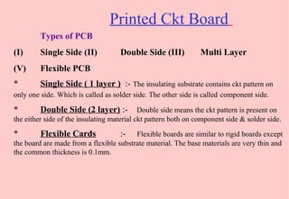
  • 1. Printed Ckt Board Types of PCB (I) Single Side (II) Double Side (III) Multi Layer (V) Flexible PCB * Single Side ( 1 layer ) :- The insulating substrate contains ckt pattern on only one side. Which is called as solder side. The other side is called component side. * Double Side (2 layer) :- Double side means the ckt pattern is present on the either side of the insulating material ckt pattern both on component side & solder side. * Flexible Cards :- Flexible boards are similar to rigid boards except the board are made from a flexible substrate material. The base materials are very thin and the common thickness is 0.1mm.
  • 2. * Multi layer Board (MLB, 4L,6L,8L,12L,16L ) :- The ckt density is high compare to D/S for inner layer made of special laminate is used for bonding purpose ( Prepreg). The inner layer is etched “CU” and outer layer is Non- etched ckt. After lamination or pressing the boards are drilled and plated like PTH D/S.
  • 3. Process Flow chart for Single Side P.C.B. Sheet Cutting Film master preparation Screen Preparation Drying Screen Printing Board cleaning Retouching Etching Drilling Ink Stripping Legend Printing Roller Tinning or HAL Masking Final Cutting Q.C.
  • 4. Process Flow Chart of Double Side P.C.B. Sheet Cutting Film Master Preparation CNC Drilling Photo Printing PTH or Electroplating Board Cleaning Pattern Plating or Electro Plating Dry film Stripping Etching H.A.L. Green Masking Tin Stripping Legend Printing Final Cutting Q.C.
  • 5. Mechanical Operation * Sheet Cutting :- Measure the size of PCB from film or Artwork. W L * Board Area Panel Sz. PCB Sz. Boarder Area * Laminates or Copper Sheet :- 1. Glass Epoxy 2. Paper fenolic 3.Teflon 4. Ceramick (CEM)
  • 6. * Glass Epoxy :- Thickness S/S 1.6 35/0 Cu Thickness Insulating Material thickness D/S 0.8-18/18 1.6-18/18 2.4-18/18 3.2-18/18 Base material is reinforced with glass fiber or paper fiber as filler and epoxy resin and the cu foil is pressured over it to get cu clad laminates. * Paper Phenolic :- Phenolic laminates are reinforced with paper fillers and the cu foil is pressed to the base material. Thickness :- Fr-2, C-8000, 1.6- 35/0------ S/S, 0.8-18/18--- D/S 1.6- 18/18-----D/S
  • 7. * Teflon Laminates :- Teflon is reinforced with glass fiber to get aminates of low dielectric constant and it is used in Radio frequency. * SHEARING MACHINE :- Used for laminate cutting for PCB production. * Manual Shearing * Motor drive Shearing. * Final Cutting i.e. cutting in finish size. * Shearing Blades :-Two Blades :- (I) Fixed Blades (ii) Movable Blades. * Punching :-Making Big hole, slot of different shape Die &Punch. 1 to 1.50
  • 8. * Blanking :- Clean Cutting operation is done with a punching tool. * Routing :- Final Cutting by CNC machine or Pin router * Drilling :- (I) Manual Drilling (ii) CNC Drilling ( Computer numeric Control) * Manual Drilling :- * Used H.S.S. Drill Bit * Speed of M/C is 6,000-16,000 RPM * Stack Drilling * Jig Drilling.
  • 9. CNC Programming & Drilling (I) Do path making (II) Focus the Hole with help of camera and monitor. (III) For time saving and maintained the accuracy. (IV) After programming Drill one Panel for checking the program. (V) Checked Missing Hole, Extra Hole,Shifting, Inter changed Hole, Drill Dia ( Drill dia checked by Hole Gauge. ) T3 T2 T1 Path Making
  • 10. * Drill Bit :- Tungsten Carbide drill bit used in CNC machine. Shank dia * In double side PCB drill dia is always 0.1mm extra from finish size. 3.175 *. Ink Stripping/ Dry film :- To remove the ink by using Naoh or Koh solution. Ink remove and the cu appears on track and pads only.
  • 11. Masking (I) Thermal Masking (II) PISM ( Photo Imagable solder Mask) # Thermal Masking :- *. Using Screen Printing. *. -ve Masking film used in thermal masking. *. Ink in paste form added Hardener and masking reducer for making liquid form. # P.I.S.M.:- * Using Photo Printing Method. * + ve Masking film used in PISM. * Panel coated with PISM ink. * Dry in oven or UV Light. * Panel develop in Na2co3 solution. # Peel off Test #. To cover the panel with insulating ink. #. To protect the cu for oxidation # To avoid the short ckt.
  • 12. Brushing (Surface Preparation) To remove the dust particles and oxide layer from the surface of panel. . *. Chemical cleaning *. Mechanical cleaning * Chemical Cleaning :- Using Alkali chemical to remove oil, grease & soil particle on the surface of laminates. * Mechanical Cleaning :- Laminate Drilling Deburing (320 grid brush) Water rinse Buffing (wet condition ) Water rinse Drying (with hot blow air )
  • 13. FILM MASTER PREPARATION * High efficiency Compact camera used for reduction and inlargement purpose. Material Used :- (I) Lith film (ii) Lith film Developer (iii) Sodium Thosulphate (iv) Developing Trays (v) Retouching Ink (vi) Retouching Brush (vii) Butter Paper * Art Work :- (I) Manual Artwork (ii) Take Design Print out * Lith film Developer :- PART- “A”(P-Methyl amino phenol sulphats PART- “B” ( Sodium Carbonate ) Temp.- 200 +-- 30 c * Fixer :- Sodium Thosulphate * Retouching :- Using Opaque ink for cover the pin holes.
  • 14. SCREEN PRINTING It is done with the help of a wooden/ Aluminum frame having a polyester cloth tightened over it. Polyester is available in different meshes. Which are indicated by “T” that indicate the number of thread gapping. Wooden frame Three methods for Screen Printing :- (I) Direct Method :- Ammonium dichromate or Potassium dichromate is mixed with super coat solution in 1:3 ratio.
  • 15. (II) Indirect Method :- Using Five Star film. * Film Develop in H202 (Hydrogen Peroxide Solution ) (III) Direct-Indirect Method :- Chromaline film is used. * Printing Ink :- Acid Resist Blue ink for Printing of Single Side PCB. * Squeegees :- The sharpness of the squeegees is very important for printing. Line sharpness. Uniform ink coating thickness and the edge definition depends on the squeegees sharpness.
  • 16. ETCHING (1)Immersion (2) Bubble (3) Splash (4) spray Etching * Ferric Chloride Etching Solution Fecl3 350-500 g/ltr HCL 60 to 65 ml/ltr Temp 200 c to 300 c Cu +Fecl3 Fecl2 +Cucl (Green Color ) * Chromic Sulfuric Acid Etchant Chromic Acid H2so4 Temp 200 to 240 g/ltr 60 to 65 ml/ltr 20 to 300 c
  • 17. * Ammonium Chloride Etchant Ammonium Bicarbonate Ammonium Nitrate Cupric Chloride Ammonium Chloride Temp 75g/ltr 80g/ltr 200g/ltr 100 to 110g/ltr 45 to 55o C * Etching Problems 1- Under Cut 2- Over Hang Over Hang :- Excess metal growth on the side of the lone is called over hang. * ( Used in Spray Etching )
  • 18. Electrolyses/ P.T.H (Plated Through Hole):- The Copper will be deposited on hole wall without electricity. * With the help of chemical reaction * 2 to 5microne Cu ( Deposit on hole wall) Most important process in double Side PCBs Process of Electrolyses 1- Debarring Drilled panel are cleaned using debarring machine which uses a 320 grade silicon carbide brush.
  • 19. 2 - Alkaline Soda Cleaning:- Ginplate CC-50 5% by volume D. I. Water 50% Temp. 26 to 70o C W. R. 1- 2 Min. 3 - Micro Etch:- Ginplate Ad-481 120-150gm/l D. I. Water To make one ltr. H2SO4 5cc /ltr. Time 2-5Min. W.R. 1Min.
  • 20. 4 - Pre-Activator The function of this bath is to initiate the reaction of catalyst. HCL 30% Remain Water D. I. Water Time 1min. 5- Activator Gin plate -additive 443 5ml/l Ginplate activator 76ml/l Time 5-6 Min. The function is to activate the entire surface including metal and base. 6- Post Activator Gin Plate PA-491 Remaining 17% D.I. Water Its function is to remove stannic layer and to increases the bonding of electrolyses cu and ensure uniform bonding.
  • 21. *. Gin Plate Cu 406A *. Gin Plate Cu 406B *. Gin Plate Cu 406C Water Time 100ml/ltr 100ml/ltr 10ml/ltr D.I. Remaining 10-12 Min. PHOTO PRINTING # Lamination :- Laminted the D/S Panel with P.P.D.F.R. Film (Phto Polymer Dry Film Resist ) (1.0,1.5,2.0 mils) Release Sheet of 1.0mil, Polthin 1.0mils #. Normalizing #. Expose in U.V. Light, used +ve Pattern (ckt) film in D/S
  • 22. #. Develop in Na2Co3 Solution , Take -ve image on Panal #. In S/S PCB -ve ckt film is used for mfg. Of S/S PCB #. Temp- 110-115 0 c Electro Plating (1) Cu Plating (2) Tin Plating * To increase the cu thickness of hole wall. H2So4 CuSo4 Cupper acid Current Time Anode Anode Bag 10% 80g/l 7cc/l 2-3 Amp/Sq.dm 15min Cu. Min-0.04-0.08% Polypropylene Anode Hook Titanium or Stainless Steel Bath Tank P.v.c.
  • 23. *. Tin Plating Stannous Sulphate H2So4 Stannous Carrer Additive Stannolume Brighter Time Anode Current Anode 30g/l 100ml/l 30ml/l 2ml/l 5min 1-2 Amp/dm2 60% Tin &40% Lead
  • 24. *. Legend Printing or Back Marking Used for identification of holes for which component can be placed .Screen Printing method for Back marking process. *. Roller Tinning Or Hot Air Levelling ( H.A.L.) To avoid the oxidation layer on Pads # Flux ( Liquid) # Sn+Pb ( Tin+ Lead) 60+40#. Temp- 2300 c to 2500 c
  • 25. *. Final Cutting ( Routing) To Cut the PCB in exact Size ad required by the customer. Quality Control (I) Checking for short ckts. (II) Checking for shifting (III) Checking for required hole dia. (IV) Checking for the proper masking. (v) Checking for final cut and above all whether the PCB is delivered in the same material as desired or not