SlideShare a Scribd company logo
1 of 2
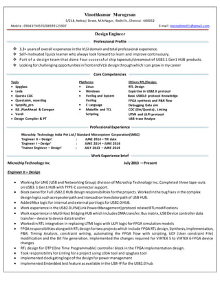
Vinothkumar Murugesan
5/218, Nethaji Street, M.A.Nagar, Redhills, Chennai -600052
Mobile : 09043794570/08939125907 E-mail: mvinothmit91@gmail.com
Design Engineer
Professional Profile
 3.3+ yearsof overall experience inthe VLSI domainandtotal professional experience.
 Self-motivated/quick learner who always look forward to learn and improve continuously.
 Part of a design team that done Four successful chip tapeouts/streamout of USB3.1 Gen1 HUB products.
 LookingforchallengingopportunitiesinfrontendVLSIdesignthroughwhichIcan grow in mycareer
Core Competencies
Tools Platforms Others RTL/Design:
 Spyglass  Linux RTL Design
 Leda  Windows Expertise in USB2.0 protocol
 Questa CDC  Verilog and System Basic USB3.0 protocol Knowledge
 Questasim, ncverilog Verilog FPGA synthesis and P&R flow
 Synplify_pro  C Language Debugging Gate sim
 ISE ,PlanAhead & Coregen  Makefile and TCL CDC (0in/Questa) , Linting
 Verdi Scripting UTMI and ULPI protocol
Design Compiler & PT USB trace Analyze
Professional Experience
Microchip Technology India Pvt Ltd / Standard Microsystem Corporation(SMSC)
‘Engineer II – Design’ : JUNE 2016 – Till date
‘Engineer I – Design’ : JUNE 2014 – JUNE 2016
‘Trainee Engineer – Design’ : JULY 2013 – JUNE 2014
Work Experience brief
MicrochipTechnology Inc July 2013 —Present
Engineer II – Design
 Workingfor UNG (USB and Networking Group) division of Microchip Technology Inc. Completed three tape-outs
on USB3. 1 Gen1 HUB with TYPE-C connector support. 
 Blockownerfor Full USB2.0 HUB design responsibilities forthe projects. Workedinthe bugfixesinthe complex
designlogicssuchasrepeaterpathand transactiontranslatorpathof USB HUB.
 AddedMux logicfor internal andexternal portlogicforUSB2.0 HUB.
 Work experience inthe USB2.0 LPM(LinkPowerManagement) protocol relatedRTLmodifications
 Work experience inMulti HostBridgingHUB whichincludesDMA transfer,Busmatrix,USBDevice controllerdata
transfer– device todevice datatransfer
 Worked in RTL integration in replacing UTMI logic with ULPI logic for FPGA simulation models
 FPGA responsibilitiesalongwithRTLdesignfortwoprojectswhich include FPGA RTLdesign,Synthesis,Implementation,
P&R, Timing Analysis, constraint writing, automating the FPGA flow with scripting, UCF (User constraint File)
modification and the Bit file generation. Implemented the changes required for VIRTEX 5 to VIRTEX 6 FPGA device
changes
 RTL design for OTP (One Time Programmable) controller block in the FPGA implementation design.
 Took responsibility for Linting for a project using LEDA tool and spyglass tool
 Implementedclockgatinglogicof the designforpowermanagement
 ImplementedEmbeddedtestfeature asavailable inthe USB-IFforthe USB2.0 hub 

 Have experience in generating clocks with DCM/MMCMfor FPGA design using Xilinx Coregen tool
 Formality Verification between Gate vs RTL.
 Done Clockdomaincrossing (CDC) flowbring-upforthe projectsusingQuestaCDCtools(0-in) 
 Gate Level Simulations on timing and functional (Zero-delay and timing annotated simulations)
 Experience indebuggingthe USBtraceswithLecroyand EllisysUSBanalyzer.
 Hands onexperienceinconnectingLogicanalyzerwithFPGA boardviaMICTORs to debugthe functionality
 USB2.0 Powerdelivery applicabletoHUB protocol workexperience
Education & Qualification
 Bachelor of Engineering in Electronics and Instrumentation Engineering, MIT campus , Anna University , Chennai, CGPA 8.79/10, 
June 2009- May 2013 
 12th
HSC, State Board, Elite Matric HSS, Red hills, 95.58%, June 2008- May2009 
 10th
SSLC, State Board, GHSS, Padiyanallur, 90.2%, June 2006- May 2007 
Rewards & Recognitions

 Received scholarship from District collector office for my SSLC examination District top ranks among all Government Schools in
Tiruvallur District 
 School First Rank :Secured my School First rank in HSC (12) and SSLC (10) examination 
 Recognized in Microchip for 3 times in the 3 year.
1. Certificate of recognition for the efforts in Tyler A0 desgin, DFT and FPGA activities
 Certificate of recognition for working on the FPGA bring up activities for the Type C hub project 
 Certificate of recognition for fixing the complex bug in ISOC 2 endpoint split transaction issue in the USB2.0 HUB Transaction
Translator logic
Personal Information
Marital Status : Single
Age : 24
Hobbies : Guitar playing andlisteningtoMelodies
Yours Faithfully,
Date:
Place: (M. VINOTHKUMAR)

More Related Content

What's hot (20)

Blake Xu Resume
Blake Xu ResumeBlake Xu Resume
Blake Xu Resume
 
Resume_Gaurav Jaiswal
Resume_Gaurav JaiswalResume_Gaurav Jaiswal
Resume_Gaurav Jaiswal
 
Mani Final Resume
Mani Final ResumeMani Final Resume
Mani Final Resume
 
akshay new-1(1)-2
akshay new-1(1)-2akshay new-1(1)-2
akshay new-1(1)-2
 
Tulika_Gupta_DFT_5yrs
Tulika_Gupta_DFT_5yrsTulika_Gupta_DFT_5yrs
Tulika_Gupta_DFT_5yrs
 
jayesh_resume
jayesh_resumejayesh_resume
jayesh_resume
 
Vinod_CV
Vinod_CVVinod_CV
Vinod_CV
 
Vivek Kotwal Resume
Vivek Kotwal ResumeVivek Kotwal Resume
Vivek Kotwal Resume
 
MohamedMustafa
MohamedMustafaMohamedMustafa
MohamedMustafa
 
Ganesh machavarapu resume
Ganesh  machavarapu resumeGanesh  machavarapu resume
Ganesh machavarapu resume
 
Broadcom Bangalore Openings
Broadcom Bangalore OpeningsBroadcom Bangalore Openings
Broadcom Bangalore Openings
 
Software analyst resume
Software analyst resumeSoftware analyst resume
Software analyst resume
 
resume
resumeresume
resume
 
Resume_Shwetabahen
Resume_ShwetabahenResume_Shwetabahen
Resume_Shwetabahen
 
updatedElectrical
updatedElectricalupdatedElectrical
updatedElectrical
 
Suraj R -resume
Suraj R -resumeSuraj R -resume
Suraj R -resume
 
My resume
My resumeMy resume
My resume
 
Resume_Akshay_Deshpande
Resume_Akshay_DeshpandeResume_Akshay_Deshpande
Resume_Akshay_Deshpande
 
NEHA JAIN_RESUME
NEHA JAIN_RESUMENEHA JAIN_RESUME
NEHA JAIN_RESUME
 
Yugandhar_01
Yugandhar_01Yugandhar_01
Yugandhar_01
 

Similar to RTL Design Engineer - Vinothkumar Murugesan - 3.3Yrs - Microchip

Similar to RTL Design Engineer - Vinothkumar Murugesan - 3.3Yrs - Microchip (20)

AzMoC++Mt
AzMoC++MtAzMoC++Mt
AzMoC++Mt
 
Ahmed Hassan CV_amin4
Ahmed Hassan CV_amin4Ahmed Hassan CV_amin4
Ahmed Hassan CV_amin4
 
ANKIT_TRIVEDI
ANKIT_TRIVEDIANKIT_TRIVEDI
ANKIT_TRIVEDI
 
Abhilash resume
Abhilash resumeAbhilash resume
Abhilash resume
 
meghana_resume
meghana_resumemeghana_resume
meghana_resume
 
Resume
ResumeResume
Resume
 
Resume
ResumeResume
Resume
 
Ankush_Goyal_Resume_2years_Exp
Ankush_Goyal_Resume_2years_ExpAnkush_Goyal_Resume_2years_Exp
Ankush_Goyal_Resume_2years_Exp
 
PrakashSahoo
PrakashSahooPrakashSahoo
PrakashSahoo
 
181114051_Intern Report (11).pdf
181114051_Intern Report (11).pdf181114051_Intern Report (11).pdf
181114051_Intern Report (11).pdf
 
Resume
ResumeResume
Resume
 
Resume
ResumeResume
Resume
 
Leela Madhavi KV_Latest
Leela Madhavi KV_LatestLeela Madhavi KV_Latest
Leela Madhavi KV_Latest
 
Vinay's_profile
Vinay's_profileVinay's_profile
Vinay's_profile
 
Sabarinath TM
Sabarinath TMSabarinath TM
Sabarinath TM
 
Resume_PraveenKumar
Resume_PraveenKumarResume_PraveenKumar
Resume_PraveenKumar
 
PrasadResume
PrasadResumePrasadResume
PrasadResume
 
ASHISH CV
ASHISH CVASHISH CV
ASHISH CV
 
pramodhk
pramodhkpramodhk
pramodhk
 
9 yrs of Testing Exp_STB and DSL gateway products
9 yrs of Testing Exp_STB and DSL gateway products9 yrs of Testing Exp_STB and DSL gateway products
9 yrs of Testing Exp_STB and DSL gateway products
 

RTL Design Engineer - Vinothkumar Murugesan - 3.3Yrs - Microchip

  • 1. Vinothkumar Murugesan 5/218, Nethaji Street, M.A.Nagar, Redhills, Chennai -600052 Mobile : 09043794570/08939125907 E-mail: mvinothmit91@gmail.com Design Engineer Professional Profile  3.3+ yearsof overall experience inthe VLSI domainandtotal professional experience.  Self-motivated/quick learner who always look forward to learn and improve continuously.  Part of a design team that done Four successful chip tapeouts/streamout of USB3.1 Gen1 HUB products.  LookingforchallengingopportunitiesinfrontendVLSIdesignthroughwhichIcan grow in mycareer Core Competencies Tools Platforms Others RTL/Design:  Spyglass  Linux RTL Design  Leda  Windows Expertise in USB2.0 protocol  Questa CDC  Verilog and System Basic USB3.0 protocol Knowledge  Questasim, ncverilog Verilog FPGA synthesis and P&R flow  Synplify_pro  C Language Debugging Gate sim  ISE ,PlanAhead & Coregen  Makefile and TCL CDC (0in/Questa) , Linting  Verdi Scripting UTMI and ULPI protocol Design Compiler & PT USB trace Analyze Professional Experience Microchip Technology India Pvt Ltd / Standard Microsystem Corporation(SMSC) ‘Engineer II – Design’ : JUNE 2016 – Till date ‘Engineer I – Design’ : JUNE 2014 – JUNE 2016 ‘Trainee Engineer – Design’ : JULY 2013 – JUNE 2014 Work Experience brief MicrochipTechnology Inc July 2013 —Present Engineer II – Design  Workingfor UNG (USB and Networking Group) division of Microchip Technology Inc. Completed three tape-outs on USB3. 1 Gen1 HUB with TYPE-C connector support.   Blockownerfor Full USB2.0 HUB design responsibilities forthe projects. Workedinthe bugfixesinthe complex designlogicssuchasrepeaterpathand transactiontranslatorpathof USB HUB.  AddedMux logicfor internal andexternal portlogicforUSB2.0 HUB.  Work experience inthe USB2.0 LPM(LinkPowerManagement) protocol relatedRTLmodifications  Work experience inMulti HostBridgingHUB whichincludesDMA transfer,Busmatrix,USBDevice controllerdata transfer– device todevice datatransfer  Worked in RTL integration in replacing UTMI logic with ULPI logic for FPGA simulation models  FPGA responsibilitiesalongwithRTLdesignfortwoprojectswhich include FPGA RTLdesign,Synthesis,Implementation, P&R, Timing Analysis, constraint writing, automating the FPGA flow with scripting, UCF (User constraint File) modification and the Bit file generation. Implemented the changes required for VIRTEX 5 to VIRTEX 6 FPGA device changes  RTL design for OTP (One Time Programmable) controller block in the FPGA implementation design.  Took responsibility for Linting for a project using LEDA tool and spyglass tool  Implementedclockgatinglogicof the designforpowermanagement  ImplementedEmbeddedtestfeature asavailable inthe USB-IFforthe USB2.0 hub  
  • 2.  Have experience in generating clocks with DCM/MMCMfor FPGA design using Xilinx Coregen tool  Formality Verification between Gate vs RTL.  Done Clockdomaincrossing (CDC) flowbring-upforthe projectsusingQuestaCDCtools(0-in)   Gate Level Simulations on timing and functional (Zero-delay and timing annotated simulations)  Experience indebuggingthe USBtraceswithLecroyand EllisysUSBanalyzer.  Hands onexperienceinconnectingLogicanalyzerwithFPGA boardviaMICTORs to debugthe functionality  USB2.0 Powerdelivery applicabletoHUB protocol workexperience Education & Qualification  Bachelor of Engineering in Electronics and Instrumentation Engineering, MIT campus , Anna University , Chennai, CGPA 8.79/10,  June 2009- May 2013   12th HSC, State Board, Elite Matric HSS, Red hills, 95.58%, June 2008- May2009   10th SSLC, State Board, GHSS, Padiyanallur, 90.2%, June 2006- May 2007  Rewards & Recognitions   Received scholarship from District collector office for my SSLC examination District top ranks among all Government Schools in Tiruvallur District   School First Rank :Secured my School First rank in HSC (12) and SSLC (10) examination   Recognized in Microchip for 3 times in the 3 year. 1. Certificate of recognition for the efforts in Tyler A0 desgin, DFT and FPGA activities  Certificate of recognition for working on the FPGA bring up activities for the Type C hub project   Certificate of recognition for fixing the complex bug in ISOC 2 endpoint split transaction issue in the USB2.0 HUB Transaction Translator logic Personal Information Marital Status : Single Age : 24 Hobbies : Guitar playing andlisteningtoMelodies Yours Faithfully, Date: Place: (M. VINOTHKUMAR)