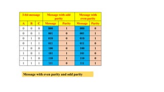
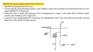
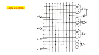
This document discusses different types of memory and programmable logic devices. It begins by explaining error detecting and correcting codes, including parity bits which allow detection of errors during transmission. It then discusses Hamming codes, which allow for both error detection and correction by including parity bits at specific bit locations. The document goes on to describe different types of read-only memory (ROM) - masked ROM, programmable ROM (PROM), erasable programmable ROM (EPROM), and electrically erasable programmable ROM (EEPROM). PROMs can be programmed by the user, EPROMs can be erased by ultraviolet light to be reprogrammed, and EEPRO
Dr. Gargi Khanna discusses error detection and correction codes such as parity codes and Hamming codes. Parity codes add an extra bit to allow detection of errors in transmitted data by checking if the total number of 1s is even or odd. Block parity codes apply this to blocks of data with row and column parity. Hamming codes can detect single and double bit errors using additional parity bits placed in specific bit locations. This allows identification and correction of single bit errors during data transmission.
This document discusses error detection and correction codes. It describes how errors can occur during digital data transmission and how extra bits are added to data to detect and sometimes correct errors. There are two types of errors: single bit errors, where one bit is changed, and burst errors, where multiple consecutive bits are changed. Error detection codes can detect errors, while error correcting codes can detect and correct errors. Common error detection techniques include parity bits and cyclic redundancy checks. Hamming codes provide error detection and correction by using parity bits located at specific bit positions to identify the location of errors.
This document discusses binary codes and their use in digital systems. It begins by defining code as the symbolic representation of discrete information elements. It then discusses various types of binary codes, including binary codes, decimal codes, Gray codes, error detection codes, and alphanumeric codes. It also discusses binary storage in registers and how information is transferred between registers in a computer's memory and processor units.
Error detection and correction codes add additional data bits to transmitted messages to detect and possibly correct errors caused by noise during transmission. Error-detecting codes only detect errors while error-correcting codes can detect and correct errors by determining the location of corrupted bits. Common techniques for error detection include parity checks, which use an extra parity bit to make the total number of 1 bits in a message either even or odd.
The document discusses error detection and correction techniques used in data transmission. It explains that errors can occur during transmission and redundancy is added through encoding schemes to detect or correct corrupted data. Error detection allows a receiver to detect if an error occurred, while error correction enables locating and replacing the exact bits in error. Block coding and convolution coding are two common coding techniques used. The document also discusses forward error correction versus retransmission for error handling.
This document discusses error detection and correction codes. It introduces parity bits which add an extra bit to allow detection of errors in binary data transmission. Hamming codes are described as allowing for both error detection and correction by adding multiple parity bits in specific locations. Finally, the document notes that Hamming codes can be modified to enable single error correction and double error detection.
to transfer data in network from one device to another with acceptable accuracy, so the system must guarantee the transmitted data should be identical to received data.
there should be no errors if any error occurs in how many ways it can be detected and corrected
Hamming code is an error-correcting code that uses additional redundant bits to detect and correct errors during data transmission. The number of redundant bits is calculated using a formula and is added to the original data bits in specific bit positions that are powers of 2. Each redundant bit checks a unique set of data bits based on their bit position. The value of the redundant bit is set to 1 if the total number of ones in the checked data bits is odd, and 0 if it is even, following the principle of even parity. This allows the detection and location of single-bit errors when the data is received.
The document discusses various types of errors that can occur during data transmission and different error detection and correction techniques. It defines transmission errors as errors caused when data is corrupted during network transmission. The main types of transmission errors are bit errors, multiple bit errors, and burst errors. Error detection techniques discussed include vertical redundancy check (VRC/parity check), longitudinal redundancy check (LRC), checksum, and cyclic redundancy check (CRC). Forward error correction techniques like Hamming codes are also summarized that allow detecting and correcting errors without retransmission.
The document summarizes various data representation techniques including Gray code, Excess-3 code, self-complementary code, weighted code, EBCDIC, and error detection codes. Gray code ensures that two successive numbers differ in only one bit. Excess-3 code represents each codeword as its decimal value plus 3 in binary. Self-complementary code allows a number to be obtained by complementing another number that adds up to 15. Weighted codes assign specific weights to each digit position. EBCDIC is an 8-bit character encoding used on IBM mainframe computers. Error detection codes add redundancy bits to facilitate error detection during data transmission.
Parity generator and checker circuits are used to detect errors in data transmission. A parity bit is added to data units using even or odd parity rules. Even parity means the total number of 1 bits including the parity bit is even. Odd parity means the total is odd. During transmission, the sender generates parity bits and the receiver checks them to detect errors. Parity can detect single bit errors but not multiple errors or errors in the parity bit itself. Integrated circuits like the 74280 TTL IC contain parity generator and checker functionality to implement error detection during data transmission.
The document discusses various data link layer protocols for medium access control in computer networks. It describes error control techniques like automatic repeat request (ARQ) and error correcting codes such as Hamming codes that allow detection and correction of errors during transmission. It also explains error detecting codes including cyclic redundancy checks (CRC) that enable detection of errors. Additionally, it covers multiple access protocols for shared mediums like Aloha, slotted Aloha, carrier sense multiple access, polling, token passing and code division multiple access.
The document discusses different types of read-only memory (ROM), including mask ROM, PROM, EPROM, and EEPROM. It explains that ROM is permanently programmed to store data that does not change, while PROM can be programmed in the field but cannot be changed after. EPROM and EEPROM can be electrically erased and reprogrammed, with EPROM also erasable by ultraviolet light. The document provides details on the memory cell structure and programming/erasure processes for each type of ROM.
International Journal of Computational Engineering Research (IJCER) is dedicated to protecting personal information and will make every reasonable effort to handle collected information appropriately. All information collected, as well as related requests, will be handled as carefully and efficiently as possible in accordance with IJCER standards for integrity and objectivity.
Satellite error detection and correction presentationAhmedMuhumed2
This document summarizes key aspects of satellite communication including error detection and correction. It discusses the elements of a digital communication system including source and channel encoders/decoders. It defines different types of errors that can occur like single bit, multiple bits, and burst errors. It then explains various error detection techniques like parity check and cyclic redundancy check (CRC). It also discusses forward error correction (FEC) where redundant bits are added to allow errors to be corrected at the receiver without retransmission. Specific error correction coding schemes like linear block codes are also summarized.
This document discusses error detection and correction techniques used in digital communication systems. It describes three types of errors that can occur during data transmission - single bit errors, multiple bit errors, and burst errors. It then explains various error detection codes like parity checking, cyclic redundancy check (CRC), longitudinal redundancy check (LRC), and checksum that are used to detect errors by adding redundancy to transmitted data. Finally, it discusses error correcting codes like Hamming codes that can detect and correct errors in the received data.
The document discusses various topics related to data link layer protocols in computer networks, including:
- Sliding window protocol which uses imaginary boxes (windows) on the sender and receiver sides to track frames and allow the sender to transmit multiple frames before requiring an acknowledgment.
- ARQ (Automatic Repeat Request) protocols like Stop-and-Wait, Go-Back-N, and Selective Repeat which determine the rules for retransmitting frames if errors are detected. Stop-and-Wait sends one frame at a time, Go-Back-N retransmits all outstanding frames, and Selective Repeat retransmits only corrupted frames.
- Piggybacking which is a technique used to improve the efficiency
The document discusses information theory and source coding. It defines information and entropy, explaining that the amount of information contained in a message depends on its probability. The entropy of a data source measures the average information content. Huffman coding is presented as a method to assign variable-length codes to symbols to minimize the average code length. Error detection and correction codes are also summarized, including parity checking, cyclic redundancy checks (CRC), linear block codes, and convolutional codes.
This document provides an introduction to a course on computer organization and assembly language. It will cover the main hardware components of a computer system, including memory, the CPU, and I/O ports. It will also discuss how instructions are executed in the fetch-execute cycle. Students will learn assembly language and how it maps to the underlying machine language understood by the CPU. They will be assessed through quizzes, assignments, a project, and a final exam.
Error detecting and correcting codes are used to detect and correct errors during data transmission. Hamming codes allow for single bit error correction and double bit error detection. Hamming codes work by assigning parity bits to specific bit positions, with each parity bit checking a set of data bit positions. If a single bit error occurs, the receiver can detect which bit is in error by checking the parity bits and make the correction. Hamming codes provide an easy way to detect and correct single bit errors during data transmission.
This document discusses error control techniques used at the data link layer. It describes different types of errors that can occur during transmission such as single bit errors and burst errors. It then explains various error detection techniques like parity checks, checksum, and cyclic redundancy check (CRC). Parity checks can detect single bit errors but not burst errors affecting an even number of bits. Checksum and CRC are more robust techniques that can detect most errors. The document also introduces error correcting codes using Hamming codes that can not only detect errors but also correct them by adding redundant bits to determine the position of the erroneous bit.
Tri-state devices are essential in bus-oriented systems to allow multiple devices to share a common bus line. A tri-state device has a high impedance state that effectively disconnects its output from the bus. This allows another device to drive the bus line without interference. Priority encoders output a binary code representing the highest priority active input. They are used in applications like interrupt controllers. Static RAM uses multiple transistors to store each bit and retains data as long as power is supplied, while dynamic RAM stores each bit in a capacitor and must be periodically refreshed to retain data.
Chapter 2-8085 Microprocessor Architecture and Microcomputer Systemscmkandemir
The 8085 microprocessor uses three separate busses - the address bus, data bus, and control bus - to perform operations. The 16-bit address bus allows the 8085 to access up to 64K memory locations. The 8-bit data bus transfers data between the microprocessor and memory or I/O devices in 8-bit chunks. The control bus consists of individual control signals that coordinate operations. Memory is organized into chips that are selected using address lines and chip select signals. This allows the microprocessor to access multiple memory chips within its 64K address range.
International Conference on NLP, Artificial Intelligence, Machine Learning an...gerogepatton
International Conference on NLP, Artificial Intelligence, Machine Learning and Applications (NLAIM 2024) offers a premier global platform for exchanging insights and findings in the theory, methodology, and applications of NLP, Artificial Intelligence, Machine Learning, and their applications. The conference seeks substantial contributions across all key domains of NLP, Artificial Intelligence, Machine Learning, and their practical applications, aiming to foster both theoretical advancements and real-world implementations. With a focus on facilitating collaboration between researchers and practitioners from academia and industry, the conference serves as a nexus for sharing the latest developments in the field.
Presentation of IEEE Slovenia CIS (Computational Intelligence Society) Chapte...University of Maribor
Slides from talk presenting:
Aleš Zamuda: Presentation of IEEE Slovenia CIS (Computational Intelligence Society) Chapter and Networking.
Presentation at IcETRAN 2024 session:
"Inter-Society Networking Panel GRSS/MTT-S/CIS
Panel Session: Promoting Connection and Cooperation"
IEEE Slovenia GRSS
IEEE Serbia and Montenegro MTT-S
IEEE Slovenia CIS
11TH INTERNATIONAL CONFERENCE ON ELECTRICAL, ELECTRONIC AND COMPUTING ENGINEERING
3-6 June 2024, Niš, Serbia
Understanding Inductive Bias in Machine LearningSUTEJAS
This presentation explores the concept of inductive bias in machine learning. It explains how algorithms come with built-in assumptions and preferences that guide the learning process. You'll learn about the different types of inductive bias and how they can impact the performance and generalizability of machine learning models.
The presentation also covers the positive and negative aspects of inductive bias, along with strategies for mitigating potential drawbacks. We'll explore examples of how bias manifests in algorithms like neural networks and decision trees.
By understanding inductive bias, you can gain valuable insights into how machine learning models work and make informed decisions when building and deploying them.
CHINA’S GEO-ECONOMIC OUTREACH IN CENTRAL ASIAN COUNTRIES AND FUTURE PROSPECTjpsjournal1
The rivalry between prominent international actors for dominance over Central Asia's hydrocarbon
reserves and the ancient silk trade route, along with China's diplomatic endeavours in the area, has been
referred to as the "New Great Game." This research centres on the power struggle, considering
geopolitical, geostrategic, and geoeconomic variables. Topics including trade, political hegemony, oil
politics, and conventional and nontraditional security are all explored and explained by the researcher.
Using Mackinder's Heartland, Spykman Rimland, and Hegemonic Stability theories, examines China's role
in Central Asia. This study adheres to the empirical epistemological method and has taken care of
objectivity. This study analyze primary and secondary research documents critically to elaborate role of
china’s geo economic outreach in central Asian countries and its future prospect. China is thriving in trade,
pipeline politics, and winning states, according to this study, thanks to important instruments like the
Shanghai Cooperation Organisation and the Belt and Road Economic Initiative. According to this study,
China is seeing significant success in commerce, pipeline politics, and gaining influence on other
governments. This success may be attributed to the effective utilisation of key tools such as the Shanghai
Cooperation Organisation and the Belt and Road Economic Initiative.
Batteries -Introduction – Types of Batteries – discharging and charging of battery - characteristics of battery –battery rating- various tests on battery- – Primary battery: silver button cell- Secondary battery :Ni-Cd battery-modern battery: lithium ion battery-maintenance of batteries-choices of batteries for electric vehicle applications.
Fuel Cells: Introduction- importance and classification of fuel cells - description, principle, components, applications of fuel cells: H2-O2 fuel cell, alkaline fuel cell, molten carbonate fuel cell and direct methanol fuel cells.
TIME DIVISION MULTIPLEXING TECHNIQUE FOR COMMUNICATION SYSTEMHODECEDSIET
Time Division Multiplexing (TDM) is a method of transmitting multiple signals over a single communication channel by dividing the signal into many segments, each having a very short duration of time. These time slots are then allocated to different data streams, allowing multiple signals to share the same transmission medium efficiently. TDM is widely used in telecommunications and data communication systems.
### How TDM Works
1. **Time Slots Allocation**: The core principle of TDM is to assign distinct time slots to each signal. During each time slot, the respective signal is transmitted, and then the process repeats cyclically. For example, if there are four signals to be transmitted, the TDM cycle will divide time into four slots, each assigned to one signal.
2. **Synchronization**: Synchronization is crucial in TDM systems to ensure that the signals are correctly aligned with their respective time slots. Both the transmitter and receiver must be synchronized to avoid any overlap or loss of data. This synchronization is typically maintained by a clock signal that ensures time slots are accurately aligned.
3. **Frame Structure**: TDM data is organized into frames, where each frame consists of a set of time slots. Each frame is repeated at regular intervals, ensuring continuous transmission of data streams. The frame structure helps in managing the data streams and maintaining the synchronization between the transmitter and receiver.
4. **Multiplexer and Demultiplexer**: At the transmitting end, a multiplexer combines multiple input signals into a single composite signal by assigning each signal to a specific time slot. At the receiving end, a demultiplexer separates the composite signal back into individual signals based on their respective time slots.
### Types of TDM
1. **Synchronous TDM**: In synchronous TDM, time slots are pre-assigned to each signal, regardless of whether the signal has data to transmit or not. This can lead to inefficiencies if some time slots remain empty due to the absence of data.
2. **Asynchronous TDM (or Statistical TDM)**: Asynchronous TDM addresses the inefficiencies of synchronous TDM by allocating time slots dynamically based on the presence of data. Time slots are assigned only when there is data to transmit, which optimizes the use of the communication channel.
### Applications of TDM
- **Telecommunications**: TDM is extensively used in telecommunication systems, such as in T1 and E1 lines, where multiple telephone calls are transmitted over a single line by assigning each call to a specific time slot.
- **Digital Audio and Video Broadcasting**: TDM is used in broadcasting systems to transmit multiple audio or video streams over a single channel, ensuring efficient use of bandwidth.
- **Computer Networks**: TDM is used in network protocols and systems to manage the transmission of data from multiple sources over a single network medium.
### Advantages of TDM
- **Efficient Use of Bandwidth**: TDM all
Redefining brain tumor segmentation: a cutting-edge convolutional neural netw...IJECEIAES
Medical image analysis has witnessed significant advancements with deep learning techniques. In the domain of brain tumor segmentation, the ability to
precisely delineate tumor boundaries from magnetic resonance imaging (MRI)
scans holds profound implications for diagnosis. This study presents an ensemble convolutional neural network (CNN) with transfer learning, integrating
the state-of-the-art Deeplabv3+ architecture with the ResNet18 backbone. The
model is rigorously trained and evaluated, exhibiting remarkable performance
metrics, including an impressive global accuracy of 99.286%, a high-class accuracy of 82.191%, a mean intersection over union (IoU) of 79.900%, a weighted
IoU of 98.620%, and a Boundary F1 (BF) score of 83.303%. Notably, a detailed comparative analysis with existing methods showcases the superiority of
our proposed model. These findings underscore the model’s competence in precise brain tumor localization, underscoring its potential to revolutionize medical
image analysis and enhance healthcare outcomes. This research paves the way
for future exploration and optimization of advanced CNN models in medical
imaging, emphasizing addressing false positives and resource efficiency.
1. UNIT V -MEMORY AND PROGRAMMABLE LOGIC
• RAM
• Memory Decoding
• Error Detection and Correction
• ROM
• Programmable Logic Array
• Programmable Array Logic
• Sequential Programmable Devices.
2. Error detecting and correcting codes
• When the digital information in the binary form is transmitted from one circuit or system to
another circuit or system an error may occur.
• This means the signal corresponding to 0 may change to 1 or vice-versa due to presence of
noise.
• To maintain data integrity between transmitter and receiver, extra bit or more than one bit are
added in the data.
• These extra bits allow the detection and sometimes the correction of error in the data.
• The data along with the extra bit /bits form the code.
• Codes which allow only error detection are called error detecting codes and codes which
allow error detection and correction are called error detecting and correcting codes.
3. Parity bit
• A parity bit is used for the purpose of detecting errors during transmission of binary information.
• A parity bit is an extra bit included with a binary message to make the number of 1s either odd or
even.
• The message including the parity bit is transmitted and then checked at the receiving end for errors.
• An error is detected if the checked parity does not correspond with the one transmitted.
• The circuit that generates the parity bit in the transmitter is called a parity generator and the circuit
that checks the parity in the receiver is called a parity checker.
• In even parity the added parity bit will make the total number of 1s an even amount. In odd parity
the added parity bit will make the total number of 1s an odd amount.
4. 3-bit message Message with odd
parity
Message with
even parity
A B C Message Parity Message Parity
0 0 0 000 1 000 0
0 0 1 001 0 001 1
0 1 0 010 0 010 1
0 1 1 011 1 011 0
1 0 0 100 0 100 1
1 0 1 101 1 101 0
1 1 0 110 1 110 0
1 1 1 111 0 111 1
Message with even parity and odd parity
5. Hamming code
• Hamming code not only provides the detection of a bit error, but also identifies which bit is in
error so that it can be corrected.
• Thus hamming code is called error detecting and correcting code.
• The code uses a number of parity bits(dependent on the number of information bits) located
at certain position in a group.
Number of parity bits:
• The number of parity bits depends on the number of information bits
• If the number of bits is designated as x, then the number of parity bits P is determined using
the relation
• 2𝑝
≥ 𝑥 + 𝑃 + 1
6. Location of the parity bits in a code:
• The parity bits are located in the positions that are numbered corresponding to ascending powers of
two(1,2,4,8,….).
• Therefore, for 7-bit code, locations for parity bits and information bits are as follows: D4, D3,D2,P3, D1,P2,P1
Assigning values to parity bit
• In hamming code , each parity bit provides a check on certain other bits in the total code, therefore we must
know the value of these others in order to assign the parity bit value.
Assignment of P1:
• This parity bit checks all bit locations, including itself, that have 1s in the same location in the binary location
numbers.
Assignment of P2:
• This parity bit checks all bit locations, including itself, that have 1s in the middle bit.
Assignment of P3:
• This parity bit checks all bit locations, including itself, that have 1s in the left-most bit.
Bit designation 𝑫𝟕 𝑫𝟔 𝑫𝟓 𝑷𝟒 𝑫𝟑 𝑷𝟐 𝑷𝟏
Bit location 7 6 5 4 3 2 1
Binary location number 111 110 101 100 011 010 001
Information bits (𝑫𝒏)
Parity bits (𝑷𝒏)
7. 1. Encode the binary word 1011 into seven bit even parity Hamming code.
Solution:
Step 1: Find the number of parity bits required. Let P=3, then
2𝑝
= 23
= 8
x+P+1=4+3+1=8
Three parity bits are sufficient.
Total code bits=4+3=7
Step 2: Construct a bit location table
Hamming code=1010101
Bit designation 𝑫𝟕 𝑫𝟔 𝑫𝟓 𝑷𝟒 𝑫𝟑 𝑷𝟐 𝑷𝟏
Bit location 7 6 5 4 3 2 1
Binary location number 111 110 101 100 011 010 001
Information bits (𝑫𝒏) 1 0 1 1
Parity bits (𝑷𝒏) 0 0 1
8. Bit designation 𝑫𝟗 𝑷𝟖 𝑫𝟕 𝑫𝟔 𝑫𝟓 𝑷𝟒 𝑫𝟑 𝑷𝟐 𝑷𝟏
Bit location 9 8 7 6 5 4 3 2 1
Binary location
number
1001 1000 0111 0110 0101 0100 0011 0010 0001
Information bits (𝑫𝒏) 1 0 1 1 1
Parity bits (𝑷𝒏) 0 1 1 0
Hamming code 1 0 0 1 1 1 1 1 0
Determine the single error-correcting code for the information code 10111 for odd parity
The Hamming code 101101101 is received. Correct it if any errors. There are four parity bits and odd parity is used.
Bit designation 𝑫𝟗 𝑷𝟖 𝑫𝟕 𝑫𝟔 𝑫𝟓 𝑷𝟒 𝑫𝟑 𝑷𝟐 𝑷𝟏
Bit location 9 8 7 6 5 4 3 2 1
Binary location
number
1001 1000 0111 0110 0101 0100 0011 0010 0001
Received code 1 0 1 1 0 1 1 0 1
9. Detect and correct error (if any) in the following received even parity hamming code word 00111101010. Also find out
the correct message.
Bit designation 𝑫𝟏𝟏 𝑫𝟏𝟎 𝑫𝟗 𝑷𝟖 𝑫𝟕 𝑫𝟔 𝑫𝟓 𝑷𝟒 𝑫𝟑 𝑷𝟐 𝑷𝟏
Bit location 11 10 9 8 7 6 5 4 3 2 1
Binary location
number
1011 1010 1001 1000 0111 0110 0101 0100 0011 0010 0001
Received code 0 0 1 1 1 1 0 1 0 1 0
Single Error Correction Plus Double Error Detection:
• A hamming code as explained above provides for the detection and correction of only a single
error. With the slight modification, it is possible to construct hamming code for single error
correction and double error detection.
• A one more parity bit is added in the hamming code to ensure hamming code (including all parity
bits) contains an even number of 1’s. The added parity bit is not used in determining the values of
the other parity bits. The resulting hamming code enables single error correction and double error
detection.
10. Given the 8-bit data word 01011011, generate the 13-bit composite word for the hamming code that corrects single
errors and detects double errors.
Bit designation 𝑷𝟏𝟑 𝑫𝟏𝟐 𝑫𝟏𝟏 𝑫𝟏𝟎 𝑫𝟗 𝑷𝟖 𝑫𝟕 𝑫𝟔 𝑫𝟓 𝑷𝟒 𝑫𝟑 𝑷𝟐 𝑷𝟏
Bit location 13 12 11 10 9 8 7 6 5 4 3 2 1
Binary location
number
1101 1100 1011 1010 1001 1000 0111 0110 0101 0100 0011 0010 0001
Information bits 0 1 0 1 1 0 1 1
Parity bits
11. Read Only Memory (ROM)
• We can't write data in read only memories.
• It is non-volatile memory i.e., it can hold data even if power is turned off.
• Generally, ROM is used to store the binary codes for the sequence of
instructions you want the computer to carry out and data such as look up
tables. This is because this type of information does not change.
• It is important to note that although we give the name RAM to static and
dynamic read/write memory devices, that does not mean that the ROMs that
we are using are also not random access devices. In fact, most ROMs are
accessed randomly with unique addresses.
• It consists of a transistor T and switch P. The transistor T is driven by the
word line. The contents of cell can be read from the cell when word line is
logic 1.
• A logic value 0 is read if the transistor is connected to ground through switch
P. If switch P is open, a logic value 1 is read. The bit line is connected
through a resistor to the power supply.
• A sense circuit at the end of the bit line generates the proper output value.
Data is stored into a ROM when it is manufactured.
• There are four types of ROM : Masked ROM, PROM, EPROM and
EEPROM or E2PROM.
12. PROM (Programmable Read Only Memory)
• PROMs are programmed by user.
• To provide the programming facility, each Address select line and data line intersection has its own
fused MOSFET or transistor.
• When the fuse is intact, the memory cell is configured as a logic 1 and when fuse is blown (open
circuit), the memory cell is logical 0.
• Logical 0s are programmed by selecting the appropriate select line and then driving the vertical
data line with a pulse of high current .
13. • It has diodes in every bit position; therefore, the
output is initially all 0s.
• Each diode, however has a fusible link in series
with it.
• By addressing bit and applying proper current
pulse at the corresponding output, we can blow
out the fuse, storing logic 1 at that bit position.
• The fuse uses material like nichrome and
polycrystalline.
• For blowing the fuse it is necessary to pass
around 20 to 50 mA of current for period 5 to 20
μs.
• The blowing of fuses according to the truth table
is called programming of ROM.
• The user can program PROMs with special
PROM programmer.
• The PROM programmer selectively burns the
fuses according to the bit pattern to be stored.
• This process is also known as burning of PROM.
• The PROMs are one time programmable.
• Once programmed, the information stored is
permanent.
14. EPROM (Erasable Programmable Read Only Memory)
• Erasable programmable ROMs use MOS circuitry.
• They store 1's and 0's as a packet of charge in a buried layer of the IC chip.
• EPROMs can be programmed by the user with a special EPROM programmer.
• The important point is that we can erase the stored data in the EPROMs by exposing the chip to ultraviolet
light through its quartz window for 15 to 20 minutes.
• It is not possible to erase selective information, when erased the entire information is lost.
• The chip can be reprogrammed.
• This memory is ideally suitable for product development, experimental projects and college laboratories, since
this chip can be reused many times, over.
15. EPROM programming :
• When erased each cell in the EPROM contains 1. Data is introduced by selectively programming 0's into the
desired bit locations. Although only 0's will be programmed, both 1's and 0's can be presented in the data.
• During programming address and data are applied to address and data pins of the EPROM.
• When the address and data are stable, program pulse is applied to the program input of the EPROM.
• The program pulse duration is around 50ms and its amplitude depends on EPROM IC.
• It is typically 5.5 V to 25 V.
• In EPROM, it is possible to program any location at any time - either individually, sequentially, or at random.
EEPROM (Electrically Erasable Programmable Read Only Memory):
• Electrically erasable programmable ROMs also use MOS circuitry very similar to that of EPROM.
• Data is stored as charge or no charge on an insulated layer or an insulated floating gate in the device.
• The insulating layer is made very thin (< 200 Å). Therefore, a voltage as low as 20 to 25 V can be used to move
charges across the thin barrier in either direction for programming or erasing.
• EEPROM allows selective erasing at the register level rather than erasing all the information since the
information can be changed by using electrical signals. The EEPROM memory also has a special chip erase
mode by which entire chip can be erased in 10 ms.
• This time is quite small as compared to time required to erase EPROM and it can be erased and reprogrammed
with device right in the circuit. However, EEPROMs are most expensive and the least dense ROMs.
16. Internal Logic of ROM
• It consists of n-input lines and m-output lines.
• Each bit combination of the input variables is called an address.
• Each bit combination that comes out of the output lines is called a word.
• The number of bits per word is equal to the number of output lines, m.
• The address specified in binary number denotes one of the minterms of n variables.
• The number of distinct addresses possible with n-input variables is 2n .
• An output word can be selected by a unique address and since there are 2n distinct addresses in ROM,
there are 2n distinct words in the ROM.
• The word available on the output lines at any given time depends on the address value applied to the
input lines.
17. • Let us consider 64 x 4 ROM.
• The ROM consists of 64 words of 4-bits each.
• This means that there are four output lines and
particular word from 64 words presently
available on the output lines is determined
from the six input lines.
• There are only six inputs in a 64 x 4 ROM
because 26 = 64 and with six variables, we can
specify 64 addresses or minterms.
• For each address input, there is a unique
selected word.
• Thus, if the input address is 000000, word
number 0 is selected and applied to output
lines.
• If the input address is 111111, word number 63
is selected and applied to output lines.
18. • The six input variables are decoded in 64 lines by means of 64 AND gates and 6 inverters.
• Each output of the decoder represents one of the minterms of a function of six variables.
• The 64 outputs of the decoder are connected through fuses to each OR gate.
• Only four of these fuse are shown in the diagram, but actually each OR gate has 64 inputs and each
input goes through a fuse that can be blown as desired.
19. • The ROM is a two level implementation in sum of minterms form.
• Let us see AND-OR and AND-OR-INVERTER implementation of ROM.
21. OR Matrix
• The OR matrix is provided to produce the logical sum of the product term outputs of the AND matrix.
• Before programming, all fuse link in OR matrix are also intact and the sum term for each OR gate is given
by,
S= P0 + P1 + .... + Pm-2+Pm-1
22. Invert/ Non-invert Matrix
• Invert/Non-invert matrix provides output in the complement or uncomplemented form.
• The user can program the output in either complement or uncomplemented form as per design
requirements.
• In both the cases if fuse is intact the output is in its uncomplemented form; otherwise output is in the
complemented form.
Combinational Logic Implementation using ROM
• Looking at the logic diagram of the ROM, we can realize that each output provides the sum of all the
minterms of n-input variables.
• We know that any Boolean function can be expressed in sum of minterms form.
• By breaking the links of those minterms not included in the function, each ROM output can be made
to represent the Boolean function of one of the output variables in the combinational circuit.
• For an n-input, m-output combinational circuit, we need a 2" x m ROM.
27. Programmable Logic Array(PLA)
• ROM,PLA and PAL (Programmable Array Logic) are the various forms of Programmable Logic
Devices(PLDs).
• PLDs can be easily configurable by the individual user for specific application.
• The combinational circuit do not use all the minterms every time.
• Occasionally, they have don't care conditions.
• Don't care condition when implemented with a ROM becomes an address input that will never occur.
• The result is that not all the bit patterns available in the ROM are used, which may be considered a waste
of available equipment.
• For cases where the number of don't care conditions is excessive, it is more economical to use a second
type of LSI component called a Programmable Logic Array (PLA).
• A PLA is similar to a ROM in concept; however it does not provide full decoding of the variables and
does not generates all the minterms as in the ROM.
• The PLA replaces decoder by group of AND gates, each of which can be programmed to generate a
product term of the input variables.
• In PLA, both AND and OR gates have fuses at the inputs, therefore in PLA both AND and OR gates are
programmable.
28. • It consists of n-inputs, output buffer with m outputs, m product terms, m sum terms, input and output
buffers.
• The product terms constitute a group of m AND gates and the sum terms constitute a group of m OR
gates, called OR matrix.
• Fuses are inserted between all n-inputs and their complement values to each of the AND gates.
• Fuses are also provided between the outputs of the AND gates and the inputs of the OR gates.
• The third set of fuses in the output inverters allows the output function to be generated either in the
AND-OR form or in the AND-OR-INVERT form.
• When inverter is bypassed by link we get AND-OR implementation.
• To get AND-OR-INVERTER implementation inverter link has to be disconnected.
29. Input Buffer
• Input buffers are provided in the PLA to limit loading of the
sources that drive the inputs.
• They also provide inverted and non-inverted form of inputs at
its output.
Output Buffer
• The driving capacity of PLA is increased by providing
buffers at the output.
• They are usually TTL compatible.
• The output buffer may provide totem-pole, open collector or
tri-state output.
30. Implementation of Combination Logic Circuit using
PLA
• Like ROM, PLA can be mask-programmable or field-
programmable.
• With a mask-programmable PLA, the user must
submit a PLA program table to the manufacturer.
• This table is used by the vendor to produce a user-
made PLA that has the required internal paths
between inputs and outputs.
• A second type of PLA available is called a Field-
Programmable Logic Array or FPLA.
• The FPLA can be programmed by the user by means
of certain recommended procedures.
• FPLAs can be programmed with commercially
available programmer units.
Example: Draw a PLA circuit to implement the logic
functions 𝑨𝑩𝑪 + 𝑨𝑩𝑪 + 𝑨𝑪 and 𝑨𝑩𝑪 + 𝑩𝑪.
Solution:
𝐴𝐵𝐶 + 𝐴𝐵𝐶 + 𝐴𝐶= 𝐴𝐵𝐶 + 𝐴(𝐵𝐶 + 𝐶)
= 𝐴𝐵𝐶 + 𝐴(𝐵 + 𝐶)
= 𝐴𝐵𝐶 + 𝐴𝐵 + 𝐴𝐶)
31. 2. Implement the following two Boolean
functions with a PLA.
𝐹1 𝐴, 𝐵, 𝐶 = Σ(0,1,2,4)
𝐹2 𝐴, 𝐵, 𝐶 = Σ(0,5,6,7)
Solution:
Step 1: Simplify the Boolean function
𝐹1 = 𝐵𝐶 + 𝐴𝐵 + 𝐴𝐶
𝐹2 = 𝐴𝐵𝐶 + 𝐴𝐶 + 𝐴𝐵
Step 2: Implementation
32. • A combinational logic circuit is defined by the following function f1(a,b,c)=∑(3,5,6,7) f2(a,b,c)=∑(0,2,4,7).
Implement the circuit with a PLA having three inputs, four product terms and two outputs.
Solution:
35. PAL(PROGRAMMABLE ARRAY LOGIC):
• It is a programmable logic device with a fixed
OR array and a programmable AND array.
• Since only AND gates are programmable, the
PAL is easier to program but it is not flexible as
PLA.
• It has four inputs and four outputs.
• Each input has buffer and an inverter gate.
38. Generate the following Boolean functions with a PAL
with 4 inputs and 4 outputs.
𝑌3 = 𝐴𝐵𝐶𝐷 + 𝐴𝐵𝐶𝐷 + 𝐴𝐵𝐶𝐷= 𝐵𝐶𝐷 + 𝐴𝐵𝐶𝐷
𝑌2 = 𝐴𝐵𝐶𝐷 + 𝐴𝐵𝐶𝐷 + 𝐴𝐵𝐶𝐷= 𝐴𝐵𝐶 + 𝐵𝐶𝐷
𝑌1 = 𝐴𝐵𝐶 + 𝐴𝐵𝐶 + 𝐴𝐵𝐶 + 𝐴𝐵𝐶= 𝐴𝐵 + 𝐴𝐵𝐶 + 𝐵𝐶
𝑌0 = 𝐴𝐵𝐶𝐷
39. • Implement the following function using PAL F1(A,B,C)=∑(1,2,4,6); F2(A,B,C)=∑(0,1,6,7);
F3(A,B,C)=∑(1,2,3,5,7)
• A combinational logic circuit is defined by the following function f1(a,b,c)=∑(0,1,6,7) f2(a,b,c)=∑(2,3,5,7).
Implement the circuit with a PAL having three inputs, three product terms and two outputs.
ROM/PROM PAL PLA
AND array is fixed and OR array is
programmable.
Both AND Programmable and OR
array is fixed.
OR and AND array is programmable.
All minterms are decoded.
Only desired minterms are
programmed using AND array.
Only desired minterms are programmed using
AND array.
Cheaper and Simpler Cheaper and Simpler Costliest and complex than PAL and PROMs
Only Boolean functions in standard SOP
form can be implemented using PROM.
Any Boolean functions in SOP
form can be implemented using
PAL.
Any Boolean functions in SOP form can be
implemented using PLA.
40. Sequential Programmable Devices
• Sequential programmable devices include both gates and flip-flops.
• Thus these devices can be used to implement sequential circuits.
• The three major types are:
Sequential (or simple) programmable logic device (SPLD)
Complex programmable logic device (CPLD)
Field‐programmable gate array (FPGA)
41. Sequential (or simple) programmable logic device (SPLD)
• The SPLD includes flip‐flops, in addition to the AND–OR array, within the integrated circuit chip
• The output is driven by an edge‐triggered D flip‐flop connected to a common clock input and changes state
on a clock edge.
• The output of the flip‐flop is connected to a three‐state buffer (or inverter) controlled by an output‐enable
signal.
• The output of the flip‐flop is fed back into one of the inputs of the programmable AND gates to provide the
present‐state condition for the sequential circuit.
42. Complex programmable logic device (CPLD)
• It is merely a collection of multiple PLDs and an interconnection structure, all on the same chip.
• In addition to individual PLDs, the on-chip interconnection structure is also programmable.
43. It consists of collection of PAL like blocks, I/O blocks and a set of interconnection wires, called
programmable interconnection structure.
The PAL like blocks are connected to the programmable interconnect structure and to the I/O blocks and it
usually consists of 16 macrocells.
The macrocells in CPLD consists of AND-OR configuration, an EX-OR gate, a flip-flop, a multiplexer and
a tri-state buffer.
The EX-OR gate provides the output of OR-gate in inverted or non-inverted form as per the fuse link
status.
A D flip flop stores the output of EX-OR gate.
Multiplexer selects either the output of the D flip flop or the output of the EX-OR gate depending on the
select input.
The tri-state buffer acts as a switch which enables or disables the output.
44.
45. Field‐programmable gate array (FPGA)
The word field refers to the ability of the gate arrays to be programmed for the specific function by the user instead
of by the manufacturer of the device.
The word array is used to indicate the series of columns and rows of gates that can be programmed by the end user.
The programmable logic blocks of FPGAs are called logic blocks or configurable logic blocks(CLBs).
The basic structure of FPGA consists of an array of logic blocks with programmable row and column
interconnecting channels surrounded by programmable I/O blocks.
46. • Look-up table (LUT) is used as a memory device that can be programmed to perform logic functions.
• Each logic block in a generic FPGA contains several logic elements.
• The logic element consists of LUT, associated logic and a flip-flop.
47. • A memory is just like a human brain. It is used to store data
and instruction. Computer memory is the storage space in
computer where data is to be processed and instructions
required for processing are stored.
• The memory is divided into large number of small parts.
Each part is called a cell. Each location or cell has a unique
address which varies from zero to memory size minus one.
• For example if computer has 64k words, then this memory
unit has 64 * 1024 = 65536 memory location. The address of
these locations varies from 0 to 65535.
• Memory is primarily of two types
Internal Memory − cache memory and primary/main
memory
External Memory − magnetic disk / optical disk etc.
48. • RAM
• A RAM constitutes the internal memory of the CPU for storing data, program and program result. It is read/write
memory. It is called random access memory (RAM).
• Since access time in RAM is independent of the address to the word that is, each storage location inside the
memory is as easy to reach as other location & takes the same amount of time. We can reach into the memory at
random & extremely fast but can also be quite expensive.
• RAM is volatile, i.e. data stored in it is lost when we switch off the computer or if there is a power failure. Hence,
a backup uninterruptible power system (UPS) is often used with computers. RAM is small, both in terms of its
physical size and in the amount of data it can hold.
• RAM is of two types
Static RAM (SRAM)
Dynamic RAM (DRAM)
49. • Static RAM (SRAM)
• The word static indicates that the memory retains its contents as long as power remains applied. However, data is
lost when the power gets down due to volatile nature. SRAM chips use a matrix of 6-transistors and no capacitors.
Transistors do not require power to prevent leakage, so SRAM need not have to be refreshed on a regular basis.
• Because of the extra space in the matrix, SRAM uses more chips than DRAM for the same amount of storage
space, thus making the manufacturing costs higher.
• Static RAM is used as cache memory needs to be very fast and small.
• Dynamic RAM (DRAM)
• DRAM, unlike SRAM, must be continually refreshed in order for it to maintain the data. This is done by placing
the memory on a refresh circuit that rewrites the data several hundred times per second. DRAM is used for most
system memory because it is cheap and small. All DRAMs are made up of memory cells. These cells are composed
of one capacitor and one transistor.
50. MEMORY DECODING
• In addition to requiring storage components in a memory unit, there is a need for
decoding circuits to select the memory word specified by the input address.
51. • When the memory enable is 0, all outputs of the decoder are 0 and none
of the memory words are selected. With the memory select at 1, one of
the four words is selected, dictated by the value in the two address lines.
• Once a word has been selected, the read/write input determines the
operation. During the read operation the four bits of the selected word go
through OR gates to the output terminals.
• During the write operation, the data available in the input lines arc
transferred into the four binary cells of the selected word. The binary
cells that are not selected are disabled and their previous binary values
remain unchanged.
• When the memory select input that goes into the decoder is equal to 0
none of the words are selected and the contents of all cells remain
unchanged regardless of the value of the read/write input.
52.
53. • Coincident Decoding
• A decoder with k inputs and 2𝑘 outputs requires 2𝑘 AND gates with k inputs per gate.
The total number of gates and the number of inputs per gate can be reduced by
employing two decoders in a two - dimensional selection scheme.
54. • Here two 2/k input decoders are used instead of one k-input decoder.
• One decoder performs the row selection and the other the column selection in a
two-dimensional matrix configuration.
• For example, instead of using a single 10 x 1,024 decoder, we use two 5 x 32
decoders.
• With the single decoder, we would need 1,024 AND gates with 10 inputs in each.
• The five most significant bits of the address go to input X and the five least
significant bits go to input Y.
• Each word within the memory array is selected by the coincidence of one X line
and one Y line.
• Thus each word in memory is selected by the coincidence between 1 of 32 rows
and 1 of 32 columns, for a total of 1,024 words.
55. Address Multiplexing
• Because of large capacity, the address decoding of DRAM is arranged in a two dimensional
array and larger memories often have multiple arrays.
• To reduce the number of pins in the IC package, designers utilize address multiplexing
whereby one set of address input pins accommodates the address components.
• In a two-dimensional array, the address is applied in two parts at different times, with the row
address first and the column address second.
• Since the same set of pins is used for both parts of the address, the size of the package is
decreased significantly.
56.
57. • The memory consists of a two-dimensional array of cells arranged into 256 rows by
256 columns, for a total of 28 x 28 = 216 = 64K words.
• There is a single data input line; a single data output line, and a read/write control as
well as an eight-bit address input and two address strobes, the latter included for-
enabling the row and column address into their respective registers.
• The row address strobe (RAS) enables the eight-bit row register and the column
address strobe (CAS) enables the eight-bit column register.
• The bar on top of the name of the strobe symbol indicates that the registers are
enabled on the zero level of the signal.