Downloaded 128 times
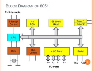
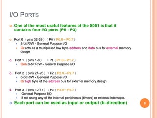
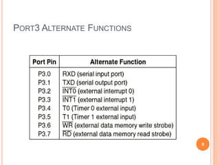
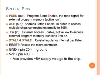
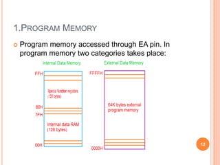
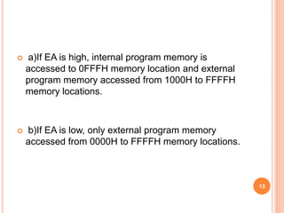


The document provides an overview of the 8051 microcontroller. It describes what a microcontroller is and lists some common uses. It then discusses the specific 8051 microcontroller, noting it was introduced by Intel in 1980 and has features like an 8-bit CPU, timers, serial port, and ability to interface with external memory. The document outlines the memory organization and I/O ports of the 8051 as well as interrupts, timers/counters, and serial communication capabilities.