Teknopark Istanbul Güncel Servis Güzergahları
•
4 likes•33,253 views

Servis Güzergahlarımız

More Related Content
What's hot
What's hot (20)
Viewers also liked
Viewers also liked (20)
More from ODTÜ TEKNOKENT YÖNETİM A.Ş.
More from ODTÜ TEKNOKENT YÖNETİM A.Ş. (20)
Teknopark Istanbul Güncel Servis Güzergahları
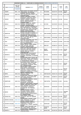
- 1. SN " GİRİŞ -ÇIKIŞ SAATLERİ TIME OF ARRIVAL - DEPARTURE GÜZERGAH / ROUTE KAPASİTE SEAT CAPACITY ŞOFÖR / DRIVER TEL / GSM PLAKA PLATE ARAÇ / VEHICLE ARAÇ TAKİP 1 ATAŞEHİR 07:55 - 17:40 DOĞU ATAŞEHİR- ATAŞEHİR MİGROS- BATI ATAŞEHİR - ATAŞEHİR TEM BAĞLANTI - TEM TEKNOPARK İSTANBUL 16 NURETTİN YILDIZ (532) 203-5721 34FL4756 MERCEDES SPRİNTER VAR 38 BEYKOZ (17:05 ÇIKIŞ) 07:25 - 17:05 BEYKOZ - ORTAÇEŞME - BEYKOZ SU ÜRÜNLERİ - PAŞABAHÇE -KAVACIK KİLER - YENİ MAH. HİSAR - TEM - TEKNOPARK İSTANBUL 16 NEŞET CANBAKIŞ (542) 240-0510 34JF9332 MERCEDES SPRİNTER VAR 7 BOSTANCI 07:55 - 17:40 BOSTANCI GÖSTERİ MERKEZİ-KÜÇÜKYALI- İDEALTEPE-MALTEPE-MALTEPE KÖPRÜSÜ E-5- CEVİZLİ E-5-KARTAL E-5 PENDİK E-5- KAYNARCA E-5 TEM BAĞLANTI YOLU- TEKNOPARK İSTANBUL 16 ERDOĞAN GENÇ (536) 499-9282 34HD8387 FIAT DUCATO VAR 25 CENNET E-5 (1. köprü) (17:05 ÇIKIŞ) 07:25 - 17:05 CENNET E-5 - SEFAKÖY E-5 - ŞİRİNEVLER E-5 - İNCİRLİ - MERTER E-5 - CEVİZLİBAĞ - AYVANSARAY -HALİÇ KÖPRÜSÜ - E-5 - 1.KÖPRÜ -TEM - TEKNOPARK İSTANBUL 27 HASAN KINAGU (530) 238-8383 34VB8946 SULTAN VAR 28 ÇAĞLAYAN ( 1.köprü ) (17:05 ÇIKIŞ) 07:25 - 17:05 SABAH: ÇAĞLAYAN E5 - MECİDİYEKÖY DURAKLAR - ORTAKLAR CAD. - MEVLÜT PEHLİVAN SOK. - VERGİ DAİRESİ DURAĞI - YILDIZ POSTA CAD. - GAYRETTEPE PTT MERKEZİ - BALMUMCU KAVŞAĞI - BARBAROS BULVARI- D-100 YILDIZ 1.KÖPRÜ BAĞLANTI YOLU - 1. KÖPRÜ - TEM - TEKNOPARK İSTANBUL AKŞAM: TEKNOPARK İSTANBUL - TEM - 1.KÖPRÜ - ZİNCİRLİKUYU - MECİDİYEKÖY DURAKLAR - ÇAĞLAYAN E-5 16 MEHMET ALİ ŞENEL (551) 207-4569 34KF3594 WOLKSVAGEN CRAFTER VAR TEKNOPARK İSTANBUL A.Ş. / SERVİS ARACI VE GÜZERGAH BİLGİLERİ / SERVICE VEHICLES AND ROUTES
- 2. 26 ÇAYIROVA 07:55 - 17:40 ÇAĞDAŞ KENT-ÇAYIROVA BELEDİYE-İNÖNÜ MAH-MUHTARLIK-ERİŞKER-ESKİ POSTAHANE- ARÇELİKYANYOL-ŞİFA MAHELLESİ İÇİ-E-5- TEKNOPARK İSTANBUL 16 ERSİN GÜZ (535) 214-5927 34KF8694 MERCEDES SPRİNTER VAR 2 ÇENGELKÖY 07:55 - 17:40 ÇENGELKÖY - NATO YOLU - ELMAKENT - DEVLET HASTANESİ SAPAĞI - ŞİLEYOLU - TEM - TEKNOPARK İSTANBUL 16 AHMET OMAK (532) 482-5762 34BGC96 MERCEDES SPRİNTER VAR 12 DARICA 07:55 - 17:40 ESKİHİSAR FERİBOT SAPAĞI - İSTASYON - BİM- DARICA ÇINAR - MEZARLIK - DARICA MEYDAN- ZİRAAT BANKASI - İYİGÜN SİTESİ - 112 EVLER - E-5 - TERSANE KÖPRÜSÜ - TEKNOPARK İSTANBUL 16 REMZİ DİLBAZ (532) 274-6271 41P0210 RENAULT MASTER 35 DARICA İSTASYON 07:55 - 17:40 İSTASYON - İŞ BANKASI - SHELL PETROL- BOLULULAR CAD. - SIRASÖĞÜTLER - NENE HATUN - BOĞAZİÇİ HAST. ARKASI - GÖKKUŞAĞI MARKET - MC DONALDS - E-5 - TERSANE KÖPRÜSÜ - TEKNOPARK İSTANBUL 16 UĞUR AKMAN (535) 676-9432 41P0694 FIAT DUCATO 4 DUDULLU 07:55 - 17:40 ÇEKMEKÖY - ŞAHİNBEY CAD. - ŞİLE OTOBANI - PAŞAKÖY YOLU- HARMANDERE- TEKNOPARK İSTANBUL 27 KASIM GÜNEŞ (543) 284-7446 34GH7473 PRESTİJ 34 ERENKÖY 07:55 - 17:40 ERENKÖY BENZİNCİ - MİNİBÜSYOLU - SAHRAYICEDİD - İNÖNÜ CAD. - ATATÜRK CAD(DÖNÜŞTE) - KOZYATAĞI - TUZCUOĞLU KÖPRÜSÜ - TEM - TEKNOPARK İSTANBUL 16 AYDIN DEMİRCİ (530) 510-4310 34BD6693 MERCEDES SPRİNTER VAR 44 ESENYALI 07:55 - 17:40 ESENYALI EVORA İSTANBUL SİTESİ - ESENYALI FATİH CAMİ - SU DEPOSU-GÜZELYALI -HEYKEL - E-5 - TERSANE KÖPRÜSÜ - TEKNOPARK İSTANBUL 16 ORHAN ARAS (536) 276-2643 34JU8486 CITROEN JUMPER VAR 37 FINDIKLI 07:55 - 17:40 YEDİTEPE ÜNİV. - FINDIKLI - İÇERENKÖY - KÜÇÜK BAKKALKÖY IŞIKLAR - ATAŞEHİR BELEDİYE - GÜMRÜK - TEM - TEKNOPARK İSTANBUL 16 SEFA DURMUŞ (545) 950-4484 34KY3564 CITROEN JUMPER VAR
- 3. 5 GEBZE 07:55 - 17:40 BELEDİYE - AKSA SAPAĞI - İBRAHİMAĞA CAD. - ŞEHİT YILMAZ ARGON CAD. - CUMA PAZARI - TRAFO - SSK - DEVELİ DURAĞI - E-5-ALEMDAR DURAĞI E-5-ŞEKERPINAR BAĞLANTI YOLU- TEM-TEKNOPARK İSTANBUL 27 NEVZAT DUMLU (535) 958-8076 41P1790 PRESTİJ VAR 57 GEBZE - TATLIKUYU 07:55 - 17:40 MUTLUKENT-HUZURKENT-KİRAZPINAR - ANİBAL-TATLIKUYU-SSK IŞIKLAR-DEVELİ DURAĞI-E-5-TEKNOPARK İSTANBUL 16 FEHMİ ŞEN (545) 236-4331 41P1791 MERCEDES SPRİNTER VAR 19 GÖZTEPE 07:55 - 17:40 GÖZTEPE - KAZASKER - AYŞEKADIN - ŞENESENEVLER - BOSTANCI DÖRTYOL - BOSTANCI LUNAPARK - BOSTANCI KÖPRÜSÜ - E5 - TEKNOPARK İSTANBUL 16 YUSUF GÜLDOĞAN (536) 300-1109 34HB2158 WOLKSVAGEN CRAFTER VAR 32 İMES 07:55 - 17:40 BARAJ YOLU - ORDU CAD - SİVAT CAD -S AMANDIRA YAN YOL -BATTALGAZİ CAD - SULTANBEYLİ YAN YOL - OSMAN GAZİ CAD - RİNGS İSTANBUL - SULTANBEYLİ YAN YOL- UYDUKENT - TEKNOPARK İSTANBUL 16 REİS YILDIRIM (532) 657-9759 34DL8558 MERCEDES SPRİNTER VAR 13 İZMİT 07:55 - 17:40 HALKEVİ - ORDU EVİ - KURUCEŞME - ÇENESUYU - DERİNCE - DOKSANBEŞEVLER - TÜTÜNÇİFTLİK - KÖRFEZ - TEM - TEKNOPARK İSTANBUL 16 ENGİN ÖRS (536) 391-5739 41P3569 MERCEDES SPRİNTER 45 KADIKÖY (17:05 ÇIKIŞ) 07:25 - 17:05 KADIKÖY RIHTIM - BELEDİYE -GÖZTEPE MİNİBÜSYOLU - ERENKÖY MİNİBÜSYOLU - BOSTANCI - BOSTANCI SAHİL -MALTEPE SAHİL - KARTAL SAHİL - PENDİK SAHİL - TERSANE KÖPRÜSÜ - TEKNOPARK İSTANBUL 16 YADİGAR SUBAŞI (532) 402-2368 34JZ1749 MERCEDES SPRİNTER VAR 17 KADIKÖY SAHİL 07:55 - 17:40 KADIKÖY BELEDİYE - KIZILTOPRAK - KALAMIŞ - FENERBAHÇE - SELAMİÇEŞME - ÇİFTEHAVUZLAR - CADDEBOSTAN - ŞAŞKINBAKKAL - BOSTANCI İSKELE - SAHİLYOLU - TERSANE KÖPRÜSÜ - 27 FAHRETTİN KARACA (541) 495-5928 34RRL84 PRESTİJ VAR 6 KADIKÖY TEM 07:55 - 17:40 KADIKÖY RIHTIM - BELEDİYE -ZİVERBEY- KUYUBAŞI - MAZHARBEY -SSK HASTANESİ-SSK HASTANESİ POLİKLİNİKLERİ - GÖZTEPE E5- TUZCUOĞLU KÖP. - TEKNOPARK İSTANBUL 16 BİLGEHAN ÖZEL (532) 496-2097 34KP9787 CITROEN JUMPER 58 KARTAL 07:55 - 17:40 KARTAL MEZARLIK KARTAL MÜNÜBÜS YOLU- KARTAL İTFAİYE - TOPSELVİ - TAVŞANTEPE - AYDINLIYOLU - KAYNARCA SSK - E5 - TERSANE KÖPRÜSÜ -TEKNOPARK İSTANBUL 16 MUSTAFA TAŞAKAN (532) 412-8781 34KP3229 FIAT DUCATO VAR 24 KOZYATAĞI CARREFOUR 07:55 - 17:40 KOZYATAĞI CARREFOUR - BOSTANCI E5- KÜÇÜKYALI E5 -MALTEPE -CEVİZLİ - TERSANE KÖPRÜSÜ - TEKNOPARK İSTANBUL 16 TAHSİN ATAK (533) 208-8817 34JL9651 WOLKSVAGEN CRAFTER VAR
- 4. 21 KOZYATAĞI E-5 (17:05 ÇIKIŞ) 07:25 - 17:05 KOZYATAĞI CARREFOUR E-5- BOSTANCI E-5- KÜÇÜKYALI E-5-MALTEPE E-5-CEVİZLİ E-5- KARTAL E-5-PENDİK E-5-KAYNARCA E-5-TEM BAĞLANTIN YOLU-TEKNOPARK İSTANBUL 27 VEDAT AVINCI (538) 968-1019 34YS995 SULTAN VAR 9 KURFALI 07:55 - 17:40 KURFALI - SPOR CAD. - CEZAEVİ - VELİBABA - AYDOS - HİLAL KONT. - ENSEY HAST. - UYDUKENT - TEKNOPARK İSTANBUL 16 MUSTAFA SARIKAYA (543) 495-5460 34EB0272 MERCEDES SPRİNTER VAR 56 KÜÇÜKBAKKALKÖY 07:55 - 17:40 KÜÇÜK BAKKALKÖY - TAÇ SPOR - BRANDIUM - GÜMRÜK - TÜRK İŞ BLOKLARI - DUDULLU CAD - BARAJ YOLU CAD - TEM TEKNOPARK İSTANBUL 16 ŞEFİK GÜNCÜ (532) 498-0036 34KL2489 CITROEN JUMPER VAR 53 KÜÇÜKYALI 07:55 - 17:40 KÜÇÜKYALI MÜNÜBÜS YOLU-MALTEPE MÜNÜBÜSYOLU-MALTEPE KÖPRÜSÜ E-5 CEVİZLİ KÖPRÜSÜ E-5 SOĞANLIK E-5-KARTAL E- 5-PENDİK E-5 TERSHANE KÖPRÜSÜ BAĞLANTI YOLU TEKNOPARK İSTANBUL 16 HAYRULLAH DERE 0535 422 8243 34HM589 CITROEN JUMPER VAR 30 LİBADİYE 07:55 - 17:40 LİBADİYE - LİBADİYE CAD. - GÖZTEPE SOYAK - BULGURLU SAPAĞI - TEM - TEKNOPARK İSTANBUL 16 ADEM KEPEZ (553) 477-9618 34RSV65 WOLKSVAGEN CRAFTER VAR 14 MALTEPE 07:55 - 17:40 MALTEPE EMNİYET - BAKKALLAR DURAĞI - GÜRAL PORSELEN - CEVİZLİ İSTASYON - TAMİRHANE - ESENTEPE MÜNÜBÜS YOLU- KARTAL SAHİL YOLU-TEKNOPARK İSTANBUL 16 MEHMET SAİT KIZILKAN (541) 730-2460 34BON21 FIAT DUCATO VAR 41 MALTEPE E-5 07:55 - 17:40 MALTEPE MERKEZ - MALTEPE MİNİBÜSYOLU - MALTEPE KÖPRÜSÜ- E-5 - MALTEPE CARREFOUR E-5 - CEVİZLİ KÖPRÜSÜ E5- KARTAL KÖPRÜSÜ E-5 - PENDİK KÖPRÜSÜ E-5 - KAYNARCA E-5 - TERSANE KÖPRÜSÜ - 16 MEHMET EMİN ALK (538) 063-5369 34UV3575 VOLKWAGEN CRAFTER VAR 33 NARCİTY 07:55 - 17:40 ZÜMRÜTEVLER ATATÜRK CAD. - NARCİTY - FUAYE SİTESİ - KİPTAŞ - YEŞİLTEPE -ADATEPE- NİŞH ADALAR - MALTEPE ORMAN YOLU - FENERBAHÇE SPOR TESİSLERİ - ORTADAĞ - SAMANDIRA TEM BAĞLANTI YOLU - TEM - 16 ADNAN İSKİPÇİ (542) 817-3237 34KP3431 FIAT DUCATO VAR 54 NAVTEK - TUZLA (18:00 TEK ÇIKIŞ ) 18:00 TEKNOPARK İSTANBUL-TEM BAĞLANTI YOLU- TESHANE KÖPRÜSÜ-GÜZELYALI KÖPRÜSÜ- İÇMELER KÖPRÜSÜ-BELEDİYE-YAYLA MAH- POSTAHANE MAH-İSTASYON MAH. 16 ENGİN DEMİR (530) 882-9961 34HT5129 MERCEDES SPRİNTER VAR
- 5. 48 OKMEYDANI (2. köprü) ( 17:05 ÇIKIŞ ) 07:25 - 17:05 OKMEYDANI KAVŞAĞI -NURTEPE TEM BAĞLANTI YOLU - HASDAL KAVŞAĞI -TEM - 4. LEVENT - 2.KÖPRÜ - TEM -TEKNOPARK İSTANBUL 16 GÖKHAN MADENDERE (542) 561-6033 34FR856 FIAT DUCATO VAR 23 ORHANLI 07:55 - 17:40 ORHANLI - AYDINLI - ÇAKAL DERESİ - FATİH MAH - ESENYALI DÖRTYOL - GÜZELYALI - TERSANE KÖPRÜSÜ - TEKNOPARK İSTANBUL 16 ERKAN ÇAKAR (532) 357-4769 34HA3203 FIAT DUCATO VAR 51 PENDİK 07:55 - 17:40 PENDİK TREN İSTASYONU-PENDİK KÖPRÜSÜ- ANKARA CAD-ÜÇEVLER-ŞEYHLİ-KURTKÖY MERKEZ-TEKNOPARK İSTANBUL 16 YUSUF BELLİ (536) 787-8203 34TS8017 FORD VAR 47 SAMANDIRA 07:55 - 17:40 SHELL PETROL-BOSNA BULVARI-FATİH BULVARI-ASIL TÜRK CAD-AYŞEGÜL SOKAK- PETROL YOLU CAD-KALE CAD-AKABE CAD- KURAN KURSU CAD-TRABZON CAD-REYHAN CAD-EŞREF BİTLİS BULVARI-DUMANKAYA 16 TACETTİN HIRDURMAZ (532) 720-7533 34VV8401 CITROEN JUMPER VAR 61 SARIGAZİ 07:55 - 17:40 SARIGAZİ-SAMANDIRA- BİLALİ HABEŞİ CAD- ALSANCAK CAD-OSMAN GAZİ CAD-AKDERE SOKAĞI-SULTANBEYLİ YANYOL-UYDUKENT- TEKNOPARK İSTANBUL 16 YUSUF YILDIZ (537) 497-8582 34GH6686 CITROEN JUMPER VAR 36 SARIYER (2.köprü) (17:05 ÇIKIŞ) 07:25 - 17:05 KOÇ ÜNİVERSİTESİ KAMPÜSÜ - RUMELİ FENERİ CAD. - SARIYER ÇAYIRBAŞI YOLU - TÜNEL - HACI OSMAN BAYIRI CAD. - BÜYÜKDERE CAD. (MASLAK) - SANAYİ -2.KÖPRÜ- TEM - TEKNOPARK İSTANBUL 16 HALIL IBRAHIM CEYLAN (532) 625-9843 34KF6052 MERCEDES SPRİNTER VAR 43 SOĞANLIK 07:55 - 17:40 SOĞANLIK - YAKACIK ÇOCUK HASTANESİ - YAKACIK MERKEZ - SPOR CAD. - VELİBABA - ANKARA CAD. - ŞIHLI - KURTKÖY MERKEZ - TEKNOPARK İSTANBUL 16 ZARİF ACET (535) 456-4062 34KK6207 CITROEN JUMPER VAR 15 ŞERİFALİ 07:55 - 17:40 DEREBOYU - ELALMIŞ CAD. - AKDAĞ CAD- HATBOYU - TEM- TEKNOPARK İSTANBUL 16 MUSTAFA TARIM (505) 708-3838 34VT3410 MERCEDES SPRİNTER VAR 39 ŞİŞLİ (1.köprü) (17:05 çıkış) 07:25 - 17:05 SABAH: ŞİŞLİ - 19 MAYIS CAD. - TÜRK KALP VAKFI - HAKKI YETEN CAD. - FULYA DERESİ SOK. - DÜNYA BARIŞ PARKI (IHLAMUR KASRI) - BEŞİKTAŞ EVLENDİRME DAİRESİ - NÜZHETİYE 16 MEHMET COSKUN (530) 928-5715 34GP3483 WOLKSVAGEN CRAFTER VAR
- 6. 42 TAŞDELEN 07:55 - 17:40 TAŞDELEN CARREFOUR - YENİDOĞAN MEZARLIK -YENİDOĞAN - YENİDOĞAN SARIGAZİ YOLU - HAKAN ŞÜKÜR STADI - SAMANDIRA MERKEZ - SULTANBEYLİ - VİAPORT - HARMANDERE -TEKNOPARK 16 MEHMET AKARSU (507) 488-4355 34VV7701 CITROEN JUMPER VAR 20 TAVUKÇU YOLU 07:55 - 17:40 SOYAK YENİŞEHİR - HATBOYU CAD. İKBAL CAD. - TAVUKÇUYOLU - İMES- TEM - TEKNOPARK İSTANBUL 16 ENES ERSOY (545) 517-3762 34VV0779 CITROEN JUMPER VAR 49 TEİ - BOSTANCI 07:15 - 16:45 BOSTANCI GÖSTERİ MERKEZİ - BOSTANCI KÖPRÜSÜ - İÇERENKÖY MEZARLIK - KÜÇÜKBAKKALKÖY YOLU - ATAŞEHİR MEMORİAL HASTANESİ - ATAŞEHİR BAĞLANTI YOLU - TEM - TEKNOPARK İSTANBUL 16 CENGİZ SÖGÜT (530) 936-5515 34LU8199 CITROEN JUMPER VAR 50 TEİ - ÜSKÜDAR 07:25 - 17:05 SABAH: E-5 KOŞUYOLU - KARACAAHMET- ÜSKÜDAR - ZEYNEP KAMİL - KARACAAHMET - E-5 - KOŞUYOLU - E-5 - ACIBADEM - GÖZTEPE - TUZCUOĞLU KÖPRÜSÜ - TEM -TEKNOPARK 16 SEBAHATTİN KENAR (532) 736-1120 34EV1291 CITROEN JUMPER 3 TEPEÜSTÜ 07:55 - 17:40 TEPEÜSTÜ - VERGİ DAİRESİ -IHLAMURKUYU - ÇAYIRÖNÜ - ADEM YAVUZ - DUDULLU - ŞİLE YOLU- KEMERDERE - MADENLER PAŞAKÖY YOLU-HARMANDERE-TEKNOPARK İSTANBUL 16 İLHAN KOZGİÇ (535) 616-9066 34NB3840 VOLKWAGEN CRAFTER VAR 8 TUZLA 07:55 - 17:40 DENİZ HARP OKULU-İTÜ-SAHİL-PAZAR YOLU- KALE KAPI-OPET-ASKERLİK ŞUBESİ-ŞOK MARKET-VATAN CAD-KAFKALE-İÇMELER- SAHİL YOLU-NEOMARİN-TEM BAĞLANTI YOLU- TEKNOPARK İSTANBUL 27 ALAATTİN ER (532) 733-4960 34FY7405 PRESTİJ VAR 52 TUZLA YAYLA 07:55 - 17:40 TUZLA MARİNA - PİYADE OKULU - VATAN CAD. YAYLA MAH - TUZLA TIP MERKEZİ - FEVZİ ÇAKMAK CAD - GÜRSEL SOK - ŞİNASİ DURAL CAD - HATBOYU CAD - TUZLA BELEDİYE - İÇMELER KÖP - E-5 - GÜZELYALI KÖP - TEM 16 ALİ SÖDEK (506) 155-9813 34KP1574 CRAFTER VAR 40 TÜCCARBAŞI 07:55 - 17:40 TÜCCARBAŞI - GÖZTEPE BENZİNLİK - MAZHARBEY - MARMARA ÜNİV. - MİNİBÜSYOLU - KUYUBAŞI IŞIKLAR -HIZIRBEY CAD. - SSK POLİKLİNİKLERİ - GÖZCÜBABA- GÖZTEPE KÖPRÜSÜ-TUZCUOĞLU KÖP.-TEM - 16 TEKİN KÖSE (532) 508-8847 34KP3244 FIAT DUCATO VAR 27 UĞUR MUMCU 07:55 - 17:40 UĞURMUMCU-YAKACIK MEYDAN-ORMAN CAD-SEMERKANT BULVARI-UGETAM-YAHYA KEMAL BEYATLI CAD-KARDELEN SOKAK- ÇİMEN SOKAK-BİMTAŞ- MİLLET CAD-OSMANLI BULVARI-HAVAALANI YOLU-TEKNOPARK 16 HAYATİ SARICA (535) 471-3895 34JC9088 MERCEDES SPRİNTER VAR 22 UYDUKENT (17:05 ÇIKIŞ) 07:25 - 17:05 DUMANKAYA KONSEPT - DOĞA KOLEJİ - YENİŞEHİR MAH. - REYHAN CAD. - CUMHURİYET CAD. - ATLANTİS - TEKNOPARK İSTANBUL 16 CENGİZ SÖĞÜT (530) 936-5515 34LU8199 FIAT DUCATO VAR
- 7. 60 UYDUKENT-ÇAMLIK 07:55 - 17:40 SEMERKANT BULVARI - SÜTCÜ İMAM CAD - SELÇUKLU CAD - SENA SOKAK - NERGİZ SOKAK -BAKÜ CAD - UYUM MARKET - MİLLET CAD - MENEKŞE SOKAK - GÜL SAKAK - MUSTAFA AKYOL SOKAK - MİLLET CAD - OSMANLI 16 BURAK TOSYALI (542) 204-8670 34NT0511 FIAT DUCATO VAR 16 ÜMRANİYE 07:55 - 17:40 EYÜPOĞLU KOLEJİ - İSTİKLAL CAD. - ATAKENT - NAMIK KEMAL - MUSTAFA KEMAL SAPAĞI TEM - TEKNOPARK İSTANBUL 16 HAMDİ AYGÜN (538) 846-7110 34KL7739 CITROEN JUMPER VAR 46 ÜMRANİYE ÇARŞI 07:55 - 17:40 NAMIK KEMAL - ÜMRANİYE DEVLET HAST. - ÜMRANİYE BELEDİYE - ÇARŞI - MARMARA CAD. - M.KEMAL SAPAĞI - TEM - TEKNOPARK İSTANBUL 16 AYDIN KOÇ (535) 202-3212 34KZ2121 WOLKSVAGEN CRAFTER VAR 31 ÜSKÜDAR İSKELE 07:55 - 17:40 ÇARŞI - AHMEDİYE - DOĞANCILAR - TUNUSBAĞI - ÇİÇEKÇİ - SELİMİYE - CEM EVİ - ZEYNEP KAMİL - E-5 -ACIBADEM KÖP. - TUZCUOĞLU KÖP. - TEM - TEKNOPARK İSTANBUL 16 HARUN AKPOLAT (542) 417-7427 34EH6169 MERCEDES SPRİNTER 18 ÜSKÜDAR TEM 07:55 - 17:40 HORHOR - TİCARET LİSESİ - SET BAŞI - FISTIK AĞACI - BAĞLARBAŞI - KOŞUYOLU CAD - ACIBADEM KÖP E5 - UZUNÇAYIR E5 - TUZCUOĞLU KÖP. - TEM - TEKNOPARK İSTANBUL 16 YUSUF AYDINLI (544) 426-6478 34SGP62 FIAT DUCATO 59 ÜSKÜDAR TEM [17:05 ÇIKIŞ ] 07:25 - 17:05 ÜSKÜDAR MERKEZ-FISTIKAĞACI-ZEYNEP KAMİL-KARACAAHMET-E-5-KOŞUYOLU E-5- ACIBADEM E-5-GÖZTEPE E-5-YENİSAHRA E-5- TUZCUOĞLU KÖPRÜSÜ- TEM-TEKNOPARK İSTANBUL 16 MAHMUT UYSAL (505) 981-6080 34PF3928 CITROEN JUMPER VAR 29 YAHYA KAPTAN 07:55 - 17:40 YAHYA KAPTAN - VİLAYET - HALKEVİ - ORDU EVİ -ACIBADEM - TEM - TEKNOPARK İSTANBUL 27 SEZGİN ÖRS (537) 815-5907 41P1671 SULTAN VAR 11 YENİSAHRA 07:55 - 17:40 YENİSAHRA E-5 - BOSTANCI E-5 - KÜÇÜKYALI E- 5 - MALTEPE E5- TERSANE KÖPRÜSÜ - TEKNOPARK İSTANBUL 16 SAVAŞ ÇELİK (537) 669-7637 34JL7400 CITROEN JUMPER VAR 55 ZEYNEP KAMİL 07:55 - 17:40 ZEYNEP KAMİL HASTANESİ-KARACA AHMET-E- 5-ACIBADEM E-5-GÖZTEPE E-5 TUZCUOĞLU KÖPRÜSÜ-TEM -TEKNOPARK İSTANBUL 16 İBRAHİM DEMİRBAŞ (535) 819-8179 34JL0856 FIAT DUCATO VAR 10 ZÜMRÜTEVLER 07:55 - 17:40 ZÜMRÜTEVLER - SOĞANLIK E5- KARTAL E-5 - PENDİK E5- KAYNARCA E5- TERSANE KÖPRÜSÜ - TEKNOPARK İSTANBUL 16 MUSTAFA TURKYILMAZ (537) 568-3855 34GKZ56 MERCEDES SPRİNTER VAR