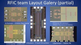
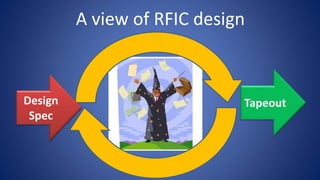
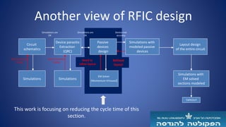
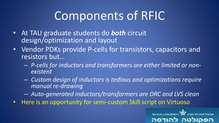
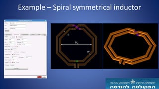
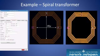
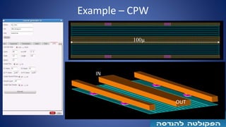
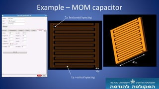
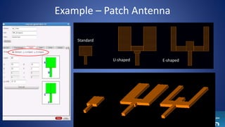
Semi-automated Layout Generation
of inductors and antennas
for 70-300Ghz
Eitan Shapira,
Avi Efrati & Michael Beeri
VLSI Lab, Physical Electronics dept
Engineering Faculty,
Tel Aviv University
Agenda
• Background
– VLSI Lab and RF Group/Lab at Tel Aviv University
• The problem – making RF layout design
by engineers more productive
• Semi-automated inductors and antenna
LAYOUT generation
Background
• Tel Aviv University (TAU) has a prestigious Engineering Faculty and EE
School
– Physical Electronics Department is part of EE school
• The VLSI Lab and RFIC Group/Lab belong to Physical Electronics
department
– Prof Arie Ruzin is the Academic Supervisor of VLSI lab, I am the Lab
engineer
– Dr. Eran Socher leads the RFIC Group/Lab (A.Drucker lab engineer)
• Numerous successful tapeouts and published papers at 100GHz-280GHz on
90nm, 65nm CMOS and SiGe
• Data presented is based on code designed by Eitan Shapira in his MSc
thesis and undergraduate project of Michael Beeri
RFIC team Layout Galery (partial)
B.Khamaisi – 233GHz freq source
I.Gertman – 70GHz PA
B.Khamaisi & S.Jameson –
233GHz freq source & Antenna
N.Buadana – Tri-band TW oscillator
A.Vishnipolski – 115GHz ILFT
A view of RFIC design
Design
Spec
Tapeout
Another view of RFIC design
Need schematics
change
Circuit
schematics
Simulations
Device parasitic
Extraction
(QRC)
Simulations
Simulations are
OK
Need schematics
change
Passive
devices
design
Simulations with
modeled passive
devices
EM Solver
(Momentum-Virtuoso)
Refined
layout
Simulations are
OK
Device met
accuracy
Layout design
of the entire circuit
Simulations with
EM solved
sections modeled
TAPEOUT
Need to
refine layout
This work is focusing on reducing the cycle time of this
section.
Components of RFIC
• At TAU graduate students do both circuit
design/optimization and layout
• Vendor PDKs provide P-cells for transistors, capacitors and
resistors but…
– P-cells for inductors and transformers are either limited or non-
existent
– Custom design of inductors is tedious and optimizations require
manual re-drawing
– Auto-generated inductors/transformers are DRC and LVS clean
• Here is an opportunity for semi-custom Skill script on Virtuoso
Example – Spiral symmetrical inductor
DIN
W
S
Example – Spiral transformer
40µ
Example – CPW
IN
OUT
100µ
Example – MOM capacitor
45µ
4µ
1µ vertical spacing
2µ horizontal spacing
Example – Patch Antenna
Standard
U-shaped E-shaped
Implementation in Skill
• I won’t talk on forms, just worked by the book
• Some parts of code used procedural style, some
parts use object-oriented style
• Basic algorithm for inductors:
– Calculate location of bend points
– Generate path thru points
– Add via arrays where needed
;-----------------------------------------------
; Class SpiralInductor
; Instance of this class represent a spiral inductor layout
;-----------------------------------------------
defclass( SpiralInductor ()
;Members
((m_layout @initarg m_layout ); The cell
(m_isSquare @initarg m_isSquare ); True if square, false if octogonal
(m_layer @initarg m_layer ); Metal layer
(m_space @initarg m_space ); Space between metals
(m_width @initarg m_width ); Metal width
(m_din @initarg m_din ); Inner diameter
(m_rounds @initarg m_rounds ); Number of rounds
(m_eddy @initarg m_eddy ); Eddy current protection (on/off)
(m_eddyLayer @initarg m_eddyLayer ); Eddy protection layer
(m_eddyDiagonal @initarg m_eddyDiagonal ); Eddy direction diagonal (on - yes/ off - no, vertical)
(m_pinsOnOff @initarg m_pinsOnOff ); True if to add pins, false if not to
(m_p1Name @initarg m_p1Name ); Name of pin 1
(m_p2Name @initarg m_p2Name ); Name of pin 2
(m_middlePoint @initarg m_middlePoint )); middle point of inductor
)
;-----------------------------------------------
; Draw the spiral inductor
;-----------------------------------------------
defmethod( Draw ((ind SpiralInductor))
if(ind->m_isSquare then
DrawSquare(ind)
else
DrawDiagonal(ind)
)
)
;-----------------------------------------------
; Draw square spiral inductor
;-----------------------------------------------
defmethod( DrawSquare ((ind SpiralInductor))
; setting the initial set of points
; The first point on the bottom middle is a little different
p_start = car(ind->m_middlePoint)+ind->m_space/2 :cadr(ind->m_middlePoint)+(ind->m_din/2)+(ind->m_width/2)
; First on bottom right corner
p1 = car(p_start)+(ind->m_din/2)+(ind->m_width/2)-(ind->m_space/2) :cadr(p_start)
…..
Points = list(p_start p1 p2 p3 p4) ;start with 5 initial points ( does not support less turns then that)
for(i 0 ind->m_rounds-2
p1 =car(p1)+ind->m_width+ind->m_space:cadr(p1)-ind->m_width-ind->m_space ;next point on the buttom right
Points = append1(Points p1)
……
)
p_end = car(p_start)-ind->m_space:cadr(p4)
Points = append1(Points p_end)
; Drawing the spiral:
MainbBox = dbCreatePath(ind->m_layout ind->m_layer Points ind->m_width)~>bBox
Future work
• Add more types of RFIC components and enhance
existing ones
• Add approximate inductance and other parameters
calculation for initial choice
– Main input remains geometry
• Add option for multi-run of EM solver with some sizes
as parameters in given range
– May require significant CPU resources…
– Possible integration with quick EM solver
Summary
• The tool shows nice results, not in production yet
– Initial version was used by Eitan Shapira in his RF research
• Working with users to add functionality
• Layout generation of most inductors and transformers
was removed from critical path of the design process
• Designer can try more layout variants towards
optimization
• The x-y stretching allows for fine tuning
Backup
RFIC mm wave design challenges
• There are many Design challenges in designing RFIC at very
high frequencies
• RFIC compounds RF and CMOS challenges:
– 100+ GHz amplifiers, VCO etc RF design
– CMOS devices limitations at 100+ GHz
– Monolithic inductors and transformers
– Ensure that Layout really implements schematics
– RC and L extraction for accurate simulation
Today I’ll focus on monolithic inductors and transformers
Goals
• Automatically generate inductors and transformers for 100-300GHz
range tailored to TSMC 65nm and easily convertible to other PDKs
• Add drop-down menu to Virtuoso which opens forms for each type
of inductor/transformer
• Interactive run-time = few seconds
– Square/octgonal inductors , stretchable x-y ratio
• Extremely streched becomes folded dipole
– Square/octgonal transformers, With/without primary/secondary
center tap
• Stretchable x-y ratio
• Option for alternating winds of primary and secondary
• Symmetrical crossings
– CPW
– Patch antenna with/without slots

TAU_Cadence2013_Final

  • 1.
    Semi-automated Layout Generation ofinductors and antennas for 70-300Ghz Eitan Shapira, Avi Efrati & Michael Beeri VLSI Lab, Physical Electronics dept Engineering Faculty, Tel Aviv University
  • 2.
    Agenda • Background – VLSILab and RF Group/Lab at Tel Aviv University • The problem – making RF layout design by engineers more productive • Semi-automated inductors and antenna LAYOUT generation
  • 3.
    Background • Tel AvivUniversity (TAU) has a prestigious Engineering Faculty and EE School – Physical Electronics Department is part of EE school • The VLSI Lab and RFIC Group/Lab belong to Physical Electronics department – Prof Arie Ruzin is the Academic Supervisor of VLSI lab, I am the Lab engineer – Dr. Eran Socher leads the RFIC Group/Lab (A.Drucker lab engineer) • Numerous successful tapeouts and published papers at 100GHz-280GHz on 90nm, 65nm CMOS and SiGe • Data presented is based on code designed by Eitan Shapira in his MSc thesis and undergraduate project of Michael Beeri
  • 4.
    RFIC team LayoutGalery (partial) B.Khamaisi – 233GHz freq source I.Gertman – 70GHz PA B.Khamaisi & S.Jameson – 233GHz freq source & Antenna N.Buadana – Tri-band TW oscillator A.Vishnipolski – 115GHz ILFT
  • 5.
    A view ofRFIC design Design Spec Tapeout
  • 6.
    Another view ofRFIC design Need schematics change Circuit schematics Simulations Device parasitic Extraction (QRC) Simulations Simulations are OK Need schematics change Passive devices design Simulations with modeled passive devices EM Solver (Momentum-Virtuoso) Refined layout Simulations are OK Device met accuracy Layout design of the entire circuit Simulations with EM solved sections modeled TAPEOUT Need to refine layout This work is focusing on reducing the cycle time of this section.
  • 7.
    Components of RFIC •At TAU graduate students do both circuit design/optimization and layout • Vendor PDKs provide P-cells for transistors, capacitors and resistors but… – P-cells for inductors and transformers are either limited or non- existent – Custom design of inductors is tedious and optimizations require manual re-drawing – Auto-generated inductors/transformers are DRC and LVS clean • Here is an opportunity for semi-custom Skill script on Virtuoso
  • 8.
    Example – Spiralsymmetrical inductor DIN W S
  • 9.
    Example – Spiraltransformer 40µ
  • 10.
  • 11.
    Example – MOMcapacitor 45µ 4µ 1µ vertical spacing 2µ horizontal spacing
  • 12.
    Example – PatchAntenna Standard U-shaped E-shaped
  • 13.
    Implementation in Skill •I won’t talk on forms, just worked by the book • Some parts of code used procedural style, some parts use object-oriented style • Basic algorithm for inductors: – Calculate location of bend points – Generate path thru points – Add via arrays where needed
  • 14.
    ;----------------------------------------------- ; Class SpiralInductor ;Instance of this class represent a spiral inductor layout ;----------------------------------------------- defclass( SpiralInductor () ;Members ((m_layout @initarg m_layout ); The cell (m_isSquare @initarg m_isSquare ); True if square, false if octogonal (m_layer @initarg m_layer ); Metal layer (m_space @initarg m_space ); Space between metals (m_width @initarg m_width ); Metal width (m_din @initarg m_din ); Inner diameter (m_rounds @initarg m_rounds ); Number of rounds (m_eddy @initarg m_eddy ); Eddy current protection (on/off) (m_eddyLayer @initarg m_eddyLayer ); Eddy protection layer (m_eddyDiagonal @initarg m_eddyDiagonal ); Eddy direction diagonal (on - yes/ off - no, vertical) (m_pinsOnOff @initarg m_pinsOnOff ); True if to add pins, false if not to (m_p1Name @initarg m_p1Name ); Name of pin 1 (m_p2Name @initarg m_p2Name ); Name of pin 2 (m_middlePoint @initarg m_middlePoint )); middle point of inductor )
  • 15.
    ;----------------------------------------------- ; Draw thespiral inductor ;----------------------------------------------- defmethod( Draw ((ind SpiralInductor)) if(ind->m_isSquare then DrawSquare(ind) else DrawDiagonal(ind) ) ) ;----------------------------------------------- ; Draw square spiral inductor ;----------------------------------------------- defmethod( DrawSquare ((ind SpiralInductor)) ; setting the initial set of points ; The first point on the bottom middle is a little different p_start = car(ind->m_middlePoint)+ind->m_space/2 :cadr(ind->m_middlePoint)+(ind->m_din/2)+(ind->m_width/2) ; First on bottom right corner p1 = car(p_start)+(ind->m_din/2)+(ind->m_width/2)-(ind->m_space/2) :cadr(p_start) ….. Points = list(p_start p1 p2 p3 p4) ;start with 5 initial points ( does not support less turns then that) for(i 0 ind->m_rounds-2 p1 =car(p1)+ind->m_width+ind->m_space:cadr(p1)-ind->m_width-ind->m_space ;next point on the buttom right Points = append1(Points p1) …… ) p_end = car(p_start)-ind->m_space:cadr(p4) Points = append1(Points p_end) ; Drawing the spiral: MainbBox = dbCreatePath(ind->m_layout ind->m_layer Points ind->m_width)~>bBox
  • 16.
    Future work • Addmore types of RFIC components and enhance existing ones • Add approximate inductance and other parameters calculation for initial choice – Main input remains geometry • Add option for multi-run of EM solver with some sizes as parameters in given range – May require significant CPU resources… – Possible integration with quick EM solver
  • 17.
    Summary • The toolshows nice results, not in production yet – Initial version was used by Eitan Shapira in his RF research • Working with users to add functionality • Layout generation of most inductors and transformers was removed from critical path of the design process • Designer can try more layout variants towards optimization • The x-y stretching allows for fine tuning
  • 18.
  • 19.
    RFIC mm wavedesign challenges • There are many Design challenges in designing RFIC at very high frequencies • RFIC compounds RF and CMOS challenges: – 100+ GHz amplifiers, VCO etc RF design – CMOS devices limitations at 100+ GHz – Monolithic inductors and transformers – Ensure that Layout really implements schematics – RC and L extraction for accurate simulation Today I’ll focus on monolithic inductors and transformers
  • 20.
    Goals • Automatically generateinductors and transformers for 100-300GHz range tailored to TSMC 65nm and easily convertible to other PDKs • Add drop-down menu to Virtuoso which opens forms for each type of inductor/transformer • Interactive run-time = few seconds – Square/octgonal inductors , stretchable x-y ratio • Extremely streched becomes folded dipole – Square/octgonal transformers, With/without primary/secondary center tap • Stretchable x-y ratio • Option for alternating winds of primary and secondary • Symmetrical crossings – CPW – Patch antenna with/without slots