SlideShare a Scribd company logo
1 of 6
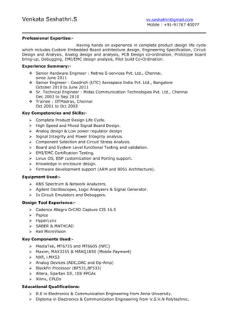
Venkata Seshathri.S sv.seshathri@gmail.com
Mobile : +91-91767 40077
Professional Expertise:-
Having hands on experience in complete product design life cycle
which includes Custom Embedded Board architecture design, Engineering Specification, Circuit
Design and Analysis, Analog design and analysis, PCB Design co-ordination, Prototype board
bring-up, Debugging, EMI/EMC design analysis, Pilot build Co-Ordination.
Experience Summary:-
 Senior Hardware Engineer : Netree E-services Pvt. Ltd., Chennai.
since June 2011
 Senior Engineer : Goodrich (UTC) Aerospace India Pvt. Ltd., Bangalore
October 2010 to June 2011
 Sr. Technical Engineer : Midas Communication Technologies Pvt. Ltd., Chennai
Dec 2003 to Sep 2010
 Trainee : IITMadras, Chennai
Oct 2001 to Oct 2003
Key Competencies and Skills:-
 Complete Product Design Life Cycle.
 High Speed and Mixed Signal Board Design.
 Analog design & Low power regulator design
 Signal Integrity and Power Integrity analysis.
 Component Selection and Circuit Stress Analysis.
 Board and System Level functional Testing and validation.
 EMI/EMC Certification Testing.
 Linux OS, BSP customization and Porting support.
 Knowledge in enclosure design.
 Firmware development support (ARM and 8051 Architecture).
Equipment Used:-
 R&S Spectrum & Network Analyzers.
 Agilent Oscilloscopes, Logic Analyzers & Signal Generator.
 In Circuit Emulators and Debuggers.
Design Tool Experience:-
 Cadence Allegro OrCAD Capture CIS 16.5
 Pspice
 HyperLynx
 SABER & MATHCAD
 Keil MicroVision
Key Components Used:-
 MediaTek, MT6735 and MT6605 (NFC)
 Maxim, MAX3255 & MAXQ1850 (Mobile Payment)
 NXP, i.MX53
 Analog Devices (ADC,DAC and Op-Amp)
 Blackfin Processor (BF531,BF533)
 Altera, Spartan IIE, IIIE FPGAs
 Xilinx, CPLDs
Educational Qualifications:
 B.E in Electronics & Communication Engineering from Anna University.
 Diploma in Electronics & Communication Engineering from V.S.V.N Polytechnic.
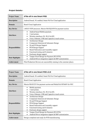
Project Details:-
Project Name d’lite all in one Smart POS
Description Android based, 3G enabled, Smart PoS for Cloud application
Domain Retail Cloud Application
Key Device i.MX53 NXP processor, Maxim MAXQ1850 for payment section
Interfaces
• Android based Mobile payment,
• 3 inch printer,
• Wireless interfaces 3G, Wi-Fi & BT,
• Voice, Ethernet, USB and Capacitive touch screen.
Responsibilities
• Architecture Design
• Component Selection & Schematic Design
• SI and PI Design Support
• PCB Design Support
• Board Fabrication and Assembly support
• Functional testing and Evaluation
• Enclosure design support
Role Highlights
• Tamper Proof Design for Payment (PCI-PTS)
• Android Driver integration support & BSP customization
Achievement Pilot Production Devices are successfully running in the customer places
Project Name d’lite all in one Smart POS v2.0
Description Android based, 3G enabled, Smart PoS for Cloud application
Domain Retail Cloud Application
Key Device Maxim MAX3255 for payment section and MediaTek MT6605 for NFC
Interfaces
• Mobile payment,
• 3 inch printer,
• Wireless interfaces 3G, Wi-Fi & BT,
• Voice, Ethernet, USB and Capacitive touch screen.
Responsibilities
• Architecture Design
• Component Selection & Schematic Design
• SI and PI Design Support
• PCB Design Support
• Board Fabrication and Assembly support
• Functional testing and Evaluation
• Enclosure design support
Role Highlights
• Tamper Proof Design for Payment (PCI-PTS)
• Android Driver integration support & BSP customization
Achievement Design completed and ready for PCB manufacturing.
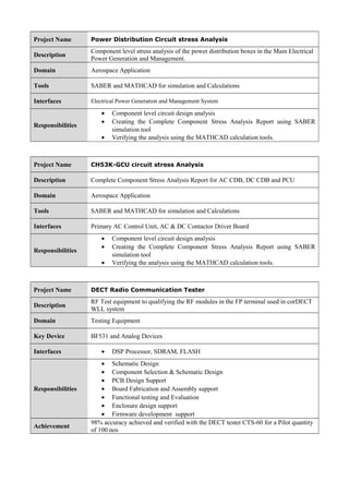
Project Name Power Distribution Circuit stress Analysis
Description
Component level stress analysis of the power distribution boxes in the Main Electrical
Power Generation and Management.
Domain Aerospace Application
Tools SABER and MATHCAD for simulation and Calculations
Interfaces Electrical Power Generation and Management System
Responsibilities
• Component level circuit design analysis
• Creating the Complete Component Stress Analysis Report using SABER
simulation tool
• Verifying the analysis using the MATHCAD calculation tools.
Project Name CH53K-GCU circuit stress Analysis
Description Complete Component Stress Analysis Report for AC CDB, DC CDB and PCU
Domain Aerospace Application
Tools SABER and MATHCAD for simulation and Calculations
Interfaces Primary AC Control Unit, AC & DC Contactor Driver Board
Responsibilities
• Component level circuit design analysis
• Creating the Complete Component Stress Analysis Report using SABER
simulation tool
• Verifying the analysis using the MATHCAD calculation tools.
Project Name DECT Radio Communication Tester
Description
RF Test equipment to qualifying the RF modules in the FP terminal used in corDECT
WLL system
Domain Testing Equipment
Key Device BF531 and Analog Devices
Interfaces • DSP Processor, SDRAM, FLASH
Responsibilities
• Schematic Design
• Component Selection & Schematic Design
• PCB Design Support
• Board Fabrication and Assembly support
• Functional testing and Evaluation
• Enclosure design support
• Firmware development support
Achievement
98% accuracy achieved and verified with the DECT tester CTS-60 for a Pilot quantity
of 100 nos
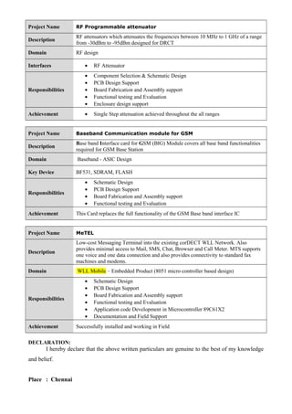
Project Name RF Programmable attenuator
Description
RF attenuators which attenuates the frequencies between 10 MHz to 1 GHz of a range
from -30dBm to -95dBm designed for DRCT
Domain RF design
Interfaces • RF Attenuator
Responsibilities
• Component Selection & Schematic Design
• PCB Design Support
• Board Fabrication and Assembly support
• Functional testing and Evaluation
• Enclosure design support
Achievement • Single Step attenuation achieved throughout the all ranges
Project Name Baseband Communication module for GSM
Description
Base band Interface card for GSM (BIG) Module covers all base band functionalities
required for GSM Base Station
Domain Baseband - ASIC Design
Key Device BF531, SDRAM, FLASH
Responsibilities
• Schematic Design
• PCB Design Support
• Board Fabrication and Assembly support
• Functional testing and Evaluation
Achievement This Card replaces the full functionality of the GSM Base band interface IC
Project Name MeTEL
Description
Low-cost Messaging Terminal into the existing corDECT WLL Network. Also
provides minimal access to Mail, SMS, Chat, Browser and Call Meter. MTS supports
one voice and one data connection and also provides connectivity to standard fax
machines and modems.
Domain WLL Mobile – Embedded Product (8051 micro controller based design)
Responsibilities
• Schematic Design
• PCB Design Support
• Board Fabrication and Assembly support
• Functional testing and Evaluation
• Application code Development in Microcontroller 89C61X2
• Documentation and Field Support
Achievement Successfully installed and working in Field
DECLARATION:
I hereby declare that the above written particulars are genuine to the best of my knowledge
and belief.
Place : Chennai
Date : 13-10-2016 ( Venkata Seshathri.S )

More Related Content

What's hot

High speed-pcb-board-design-and-analysiscadence-130218085524-phpapp01
High speed-pcb-board-design-and-analysiscadence-130218085524-phpapp01High speed-pcb-board-design-and-analysiscadence-130218085524-phpapp01
High speed-pcb-board-design-and-analysiscadence-130218085524-phpapp01khalid noman husainy
 
LTTS_Dinesh Prasath_Resume
LTTS_Dinesh Prasath_ResumeLTTS_Dinesh Prasath_Resume
LTTS_Dinesh Prasath_ResumeDinesh Prasath
 
Hardware Software Co-Design - White Paper
Hardware Software Co-Design - White PaperHardware Software Co-Design - White Paper
Hardware Software Co-Design - White PaperMistral Solutions
 
Resume analog
Resume analogResume analog
Resume analogtarora1
 
System on Chip (SoC) for mobile phones
System on Chip (SoC) for mobile phonesSystem on Chip (SoC) for mobile phones
System on Chip (SoC) for mobile phonesJeffrey Funk
 
Ball Systems Capabilities
Ball Systems CapabilitiesBall Systems Capabilities
Ball Systems Capabilitiesamhoff
 
Curriculum Vitae ganesh with photo-1
Curriculum Vitae ganesh with photo-1Curriculum Vitae ganesh with photo-1
Curriculum Vitae ganesh with photo-1Ganesh Sankar
 
Webinar on Latency and throughput computation of automotive EE network
Webinar on Latency and throughput computation of automotive EE networkWebinar on Latency and throughput computation of automotive EE network
Webinar on Latency and throughput computation of automotive EE networkDeepak Shankar
 
Design & simulation capability
Design & simulation capabilityDesign & simulation capability
Design & simulation capabilityrogercooke
 
Resume digital
Resume digitalResume digital
Resume digitaltarora1
 
Electronic Hardware Design with FPGA
Electronic Hardware Design with FPGAElectronic Hardware Design with FPGA
Electronic Hardware Design with FPGAKrishna Gaihre
 
Network programming
Network programmingNetwork programming
Network programmingAmit Dahal
 
Resume mixed signal
Resume mixed signalResume mixed signal
Resume mixed signaltarora1
 
Sunil Senior NE 092015
Sunil Senior NE 092015 Sunil Senior NE 092015
Sunil Senior NE 092015 Sunil Vasudev
 

What's hot (19)

High speed-pcb-board-design-and-analysis
High speed-pcb-board-design-and-analysis High speed-pcb-board-design-and-analysis
High speed-pcb-board-design-and-analysis
 
High speed-pcb-board-design-and-analysiscadence-130218085524-phpapp01
High speed-pcb-board-design-and-analysiscadence-130218085524-phpapp01High speed-pcb-board-design-and-analysiscadence-130218085524-phpapp01
High speed-pcb-board-design-and-analysiscadence-130218085524-phpapp01
 
FPGA Embedded Design
FPGA Embedded DesignFPGA Embedded Design
FPGA Embedded Design
 
LTTS_Dinesh Prasath_Resume
LTTS_Dinesh Prasath_ResumeLTTS_Dinesh Prasath_Resume
LTTS_Dinesh Prasath_Resume
 
Hardware Software Co-Design - White Paper
Hardware Software Co-Design - White PaperHardware Software Co-Design - White Paper
Hardware Software Co-Design - White Paper
 
Resume analog
Resume analogResume analog
Resume analog
 
vlsi
vlsivlsi
vlsi
 
System on Chip (SoC) for mobile phones
System on Chip (SoC) for mobile phonesSystem on Chip (SoC) for mobile phones
System on Chip (SoC) for mobile phones
 
VLSI GDI Technology
VLSI GDI TechnologyVLSI GDI Technology
VLSI GDI Technology
 
Ball Systems Capabilities
Ball Systems CapabilitiesBall Systems Capabilities
Ball Systems Capabilities
 
Curriculum Vitae ganesh with photo-1
Curriculum Vitae ganesh with photo-1Curriculum Vitae ganesh with photo-1
Curriculum Vitae ganesh with photo-1
 
Webinar on Latency and throughput computation of automotive EE network
Webinar on Latency and throughput computation of automotive EE networkWebinar on Latency and throughput computation of automotive EE network
Webinar on Latency and throughput computation of automotive EE network
 
Design & simulation capability
Design & simulation capabilityDesign & simulation capability
Design & simulation capability
 
Resume digital
Resume digitalResume digital
Resume digital
 
Electronic Hardware Design with FPGA
Electronic Hardware Design with FPGAElectronic Hardware Design with FPGA
Electronic Hardware Design with FPGA
 
Network programming
Network programmingNetwork programming
Network programming
 
Resume mixed signal
Resume mixed signalResume mixed signal
Resume mixed signal
 
Deep_resume
Deep_resumeDeep_resume
Deep_resume
 
Sunil Senior NE 092015
Sunil Senior NE 092015 Sunil Senior NE 092015
Sunil Senior NE 092015
 

Viewers also liked

Viewers also liked (11)

Astrocol
AstrocolAstrocol
Astrocol
 
Diapositivas
DiapositivasDiapositivas
Diapositivas
 
Árbol de predicción
Árbol de predicciónÁrbol de predicción
Árbol de predicción
 
Diapositivas
DiapositivasDiapositivas
Diapositivas
 
مستلزمات الترسيم
مستلزمات الترسيممستلزمات الترسيم
مستلزمات الترسيم
 
Inovacion e invencion
Inovacion e invencionInovacion e invencion
Inovacion e invencion
 
AMJED KAZEM HASAN
AMJED KAZEM HASANAMJED KAZEM HASAN
AMJED KAZEM HASAN
 
Paulo freire
Paulo freirePaulo freire
Paulo freire
 
Power prezzi
Power prezziPower prezzi
Power prezzi
 
RLNarodowg_Resume
RLNarodowg_ResumeRLNarodowg_Resume
RLNarodowg_Resume
 
Labord. evaluation-par-les-pairs -MOOC-pedagogie
Labord. evaluation-par-les-pairs -MOOC-pedagogieLabord. evaluation-par-les-pairs -MOOC-pedagogie
Labord. evaluation-par-les-pairs -MOOC-pedagogie
 

Similar to SVS_Resume

Similar to SVS_Resume (20)

Resume_DharshanBM
Resume_DharshanBMResume_DharshanBM
Resume_DharshanBM
 
Hardware Design engineer
Hardware Design engineerHardware Design engineer
Hardware Design engineer
 
Vinay_CV
Vinay_CVVinay_CV
Vinay_CV
 
Resume_Bhasker
Resume_BhaskerResume_Bhasker
Resume_Bhasker
 
Embedded System and IoT - ALTEN Calsoft Labs
Embedded System and IoT - ALTEN Calsoft LabsEmbedded System and IoT - ALTEN Calsoft Labs
Embedded System and IoT - ALTEN Calsoft Labs
 
Detailed Cv
Detailed CvDetailed Cv
Detailed Cv
 
VIKAS _SENIOR HARDWARE
VIKAS _SENIOR HARDWAREVIKAS _SENIOR HARDWARE
VIKAS _SENIOR HARDWARE
 
Edwin Vinoth_Resume
Edwin Vinoth_ResumeEdwin Vinoth_Resume
Edwin Vinoth_Resume
 
Traditional vs. SoC FPGA Design Flow A Video Pipeline Case Study
Traditional vs. SoC FPGA Design Flow A Video Pipeline Case StudyTraditional vs. SoC FPGA Design Flow A Video Pipeline Case Study
Traditional vs. SoC FPGA Design Flow A Video Pipeline Case Study
 
RESUME
RESUMERESUME
RESUME
 
RESUME
RESUMERESUME
RESUME
 
Creating Digital Experience in PCB Designs 2019
Creating Digital Experience in PCB Designs 2019Creating Digital Experience in PCB Designs 2019
Creating Digital Experience in PCB Designs 2019
 
William Check Resume
William Check ResumeWilliam Check Resume
William Check Resume
 
Pratik Shah_Revised Resume
Pratik Shah_Revised ResumePratik Shah_Revised Resume
Pratik Shah_Revised Resume
 
GeneCernilliResume
GeneCernilliResumeGeneCernilliResume
GeneCernilliResume
 
Resume-Shams_v3
Resume-Shams_v3Resume-Shams_v3
Resume-Shams_v3
 
VLMADHUSUDAN Resume
VLMADHUSUDAN ResumeVLMADHUSUDAN Resume
VLMADHUSUDAN Resume
 
Presentation Cable Project Cad Adc
Presentation Cable Project Cad AdcPresentation Cable Project Cad Adc
Presentation Cable Project Cad Adc
 
Anbazhagan_Resume
Anbazhagan_ResumeAnbazhagan_Resume
Anbazhagan_Resume
 
Jay_Vicory_Resume_2018
Jay_Vicory_Resume_2018Jay_Vicory_Resume_2018
Jay_Vicory_Resume_2018
 

SVS_Resume

  • 1. Venkata Seshathri.S sv.seshathri@gmail.com Mobile : +91-91767 40077 Professional Expertise:- Having hands on experience in complete product design life cycle which includes Custom Embedded Board architecture design, Engineering Specification, Circuit Design and Analysis, Analog design and analysis, PCB Design co-ordination, Prototype board bring-up, Debugging, EMI/EMC design analysis, Pilot build Co-Ordination. Experience Summary:-  Senior Hardware Engineer : Netree E-services Pvt. Ltd., Chennai. since June 2011  Senior Engineer : Goodrich (UTC) Aerospace India Pvt. Ltd., Bangalore October 2010 to June 2011  Sr. Technical Engineer : Midas Communication Technologies Pvt. Ltd., Chennai Dec 2003 to Sep 2010  Trainee : IITMadras, Chennai Oct 2001 to Oct 2003 Key Competencies and Skills:-  Complete Product Design Life Cycle.  High Speed and Mixed Signal Board Design.  Analog design & Low power regulator design  Signal Integrity and Power Integrity analysis.  Component Selection and Circuit Stress Analysis.  Board and System Level functional Testing and validation.  EMI/EMC Certification Testing.  Linux OS, BSP customization and Porting support.  Knowledge in enclosure design.  Firmware development support (ARM and 8051 Architecture). Equipment Used:-  R&S Spectrum & Network Analyzers.  Agilent Oscilloscopes, Logic Analyzers & Signal Generator.  In Circuit Emulators and Debuggers. Design Tool Experience:-  Cadence Allegro OrCAD Capture CIS 16.5  Pspice  HyperLynx  SABER & MATHCAD  Keil MicroVision Key Components Used:-  MediaTek, MT6735 and MT6605 (NFC)  Maxim, MAX3255 & MAXQ1850 (Mobile Payment)  NXP, i.MX53  Analog Devices (ADC,DAC and Op-Amp)  Blackfin Processor (BF531,BF533)  Altera, Spartan IIE, IIIE FPGAs  Xilinx, CPLDs Educational Qualifications:  B.E in Electronics & Communication Engineering from Anna University.  Diploma in Electronics & Communication Engineering from V.S.V.N Polytechnic.
  • 2. Project Details:- Project Name d’lite all in one Smart POS Description Android based, 3G enabled, Smart PoS for Cloud application Domain Retail Cloud Application Key Device i.MX53 NXP processor, Maxim MAXQ1850 for payment section Interfaces • Android based Mobile payment, • 3 inch printer, • Wireless interfaces 3G, Wi-Fi & BT, • Voice, Ethernet, USB and Capacitive touch screen. Responsibilities • Architecture Design • Component Selection & Schematic Design • SI and PI Design Support • PCB Design Support • Board Fabrication and Assembly support • Functional testing and Evaluation • Enclosure design support Role Highlights • Tamper Proof Design for Payment (PCI-PTS) • Android Driver integration support & BSP customization Achievement Pilot Production Devices are successfully running in the customer places Project Name d’lite all in one Smart POS v2.0 Description Android based, 3G enabled, Smart PoS for Cloud application Domain Retail Cloud Application Key Device Maxim MAX3255 for payment section and MediaTek MT6605 for NFC Interfaces • Mobile payment, • 3 inch printer, • Wireless interfaces 3G, Wi-Fi & BT, • Voice, Ethernet, USB and Capacitive touch screen. Responsibilities • Architecture Design • Component Selection & Schematic Design • SI and PI Design Support • PCB Design Support • Board Fabrication and Assembly support • Functional testing and Evaluation • Enclosure design support Role Highlights • Tamper Proof Design for Payment (PCI-PTS) • Android Driver integration support & BSP customization Achievement Design completed and ready for PCB manufacturing.
  • 3. Project Name Power Distribution Circuit stress Analysis Description Component level stress analysis of the power distribution boxes in the Main Electrical Power Generation and Management. Domain Aerospace Application Tools SABER and MATHCAD for simulation and Calculations Interfaces Electrical Power Generation and Management System Responsibilities • Component level circuit design analysis • Creating the Complete Component Stress Analysis Report using SABER simulation tool • Verifying the analysis using the MATHCAD calculation tools. Project Name CH53K-GCU circuit stress Analysis Description Complete Component Stress Analysis Report for AC CDB, DC CDB and PCU Domain Aerospace Application Tools SABER and MATHCAD for simulation and Calculations Interfaces Primary AC Control Unit, AC & DC Contactor Driver Board Responsibilities • Component level circuit design analysis • Creating the Complete Component Stress Analysis Report using SABER simulation tool • Verifying the analysis using the MATHCAD calculation tools. Project Name DECT Radio Communication Tester Description RF Test equipment to qualifying the RF modules in the FP terminal used in corDECT WLL system Domain Testing Equipment Key Device BF531 and Analog Devices Interfaces • DSP Processor, SDRAM, FLASH Responsibilities • Schematic Design • Component Selection & Schematic Design • PCB Design Support • Board Fabrication and Assembly support • Functional testing and Evaluation • Enclosure design support • Firmware development support Achievement 98% accuracy achieved and verified with the DECT tester CTS-60 for a Pilot quantity of 100 nos
  • 4. Project Name RF Programmable attenuator Description RF attenuators which attenuates the frequencies between 10 MHz to 1 GHz of a range from -30dBm to -95dBm designed for DRCT Domain RF design Interfaces • RF Attenuator Responsibilities • Component Selection & Schematic Design • PCB Design Support • Board Fabrication and Assembly support • Functional testing and Evaluation • Enclosure design support Achievement • Single Step attenuation achieved throughout the all ranges Project Name Baseband Communication module for GSM Description Base band Interface card for GSM (BIG) Module covers all base band functionalities required for GSM Base Station Domain Baseband - ASIC Design Key Device BF531, SDRAM, FLASH Responsibilities • Schematic Design • PCB Design Support • Board Fabrication and Assembly support • Functional testing and Evaluation Achievement This Card replaces the full functionality of the GSM Base band interface IC Project Name MeTEL Description Low-cost Messaging Terminal into the existing corDECT WLL Network. Also provides minimal access to Mail, SMS, Chat, Browser and Call Meter. MTS supports one voice and one data connection and also provides connectivity to standard fax machines and modems. Domain WLL Mobile – Embedded Product (8051 micro controller based design) Responsibilities • Schematic Design • PCB Design Support • Board Fabrication and Assembly support • Functional testing and Evaluation • Application code Development in Microcontroller 89C61X2 • Documentation and Field Support Achievement Successfully installed and working in Field DECLARATION: I hereby declare that the above written particulars are genuine to the best of my knowledge and belief. Place : Chennai
  • 5. Date : 13-10-2016 ( Venkata Seshathri.S )
  • 6. Date : 13-10-2016 ( Venkata Seshathri.S )