SlideShare a Scribd company logo
Surface Texturing by rapid scanning of
pulsed laser beam
Di Liu, Matthew Quigley
Advisor: Dr. David Hwang
Annual Student Research Poster
Symposium, May 10, 2013
Department of Mechanical
Engineering
College of Engineering and
Applied Sciences (CEAS)
Surface texturing in micro/nanoscale plays an important role in many application fields
including enhanced light trapping in solar cell, surface anti-icing by super hydrophobicity in
wind turbine and airplane wings, and enhanced convective and radiative heat transfer from
surface. In this study, we demonstrate high flexibility and control precision offered by the
pulsed laser scanning method. Compared with conventional laser-based approach,
nanosecond laser scanning method we tested corresponds to a highly cost-effective and
uniform means for the texturing of arbitrary sample area and shape. Relevant texturing
mechanisms are explained based on advanced characterization by scanning electron
microscope and Raman spectroscopy.
Acknowledgement
Summary
• Rapid laser scanning enabled superior textured surfaces for solar & military applications.
• Detailed texturing mechanisms were investigated in relation to target device performance.
• For solar cell, light trapping was greatly enhanced with optimal crystalline structures.
• For military applications, desired stealth and thermo-fluidic functions were enabled.
*. The research is supported by Yuco optics corp. (Bohemia, NY) through SPIR program, and Advanced Energy
Research and Technology Center (Stony Brook, NY).
*. SEM characterization was performed at the Center for Functional Nanomaterials, Brookhaven National
Laboratory supported by US Department of Energy.
New Approach : Rapid scanning of pulsed laser beam
Conventional surface texturing techniques
By D. Neuhaus et al. (2007)By D. Yong Wu et al. (2007)
By L. Dobrzaǹski et al. (2008) By SiOnyx
Ti c-Si c-Si c-Si
Chemical Wet Etching
• Limited flexibility as
crystalline plane
dictates
Laser Ablative Texturing
• Loose structural: issues
on carrier transport and
limit in current extraction
Ultrafast Laser Texturing
• High laser cost, lack of
arbitrary scale
uniformity
Mechanical Roughing
• Quality limited due
to friction with
abrasive particles
Experimental setup
Effect of laser parameters : 3 representative regimes
Ablation dominant
• Excellent light trapping
• Structural issues
Melting dominant
• Excellent light trapping
• Favorable structures
Mild melting
• Insufficient light trapping
• Low textures
Spectral reflectance data show Performance
of Black Si depending on laser parameters
Silicon surface texturing for enhanced light trapping
Si surface morphology results comparison
*Different optical properties are achieved by different surface texture structures
*Brown Silicon is formed and dominated by ablative phase change
*Shorter wavelength gives smaller scale of spikes and shallower affected depth
Brown Si Black Si
λ=355nm
Super black metal surface texturing by laser scanning
Black Cu SEM image
http://en.wikipedia.org/wiki/F-117_Nighthawk
http://thegundeck.blogspot.com/2011/01/how-
much-for-pentagon.html
Black Silicon for advanced Si solar cells
• Laser-based texturing
• High flexibility and control precision
Light trapping enhancement
Stealth function : minimal reflection
of UV, visible and IR illumination
Enforcing Pool
boiling for improved
heat transfer by
phase change
http://www.81.net/hangkongdongtai/04262301
92013_3.html
http://isnps.unm.edu/research/facilities/
IR image
Cu
Blackbody-like
Thermal Emission
Key Advantages
• Size independent uniformity
• Precision texture control:
active control of unit features
dictated by local melting and
thermo-capillary effect
• Simultaneous annealing for
improved carrier diffusion
• Cost-effective laser solution
Photograph
image
SEM image
• Ablation dominant regime is
superior in light trapping but with
low crystalline quality
• Melting dominant regime show
good light trapping and excellent
crystalline quality
Improved heat transfer and control of
phase change (cooling, anti-freezing)
Transient behavior during laser process
Necessary
ablation
for spikes
formation
Secondary annealing for efficient current extraction
On Laser focus
Off Laser focus
Laser focal position effects on secondary annealing
Extended
laser
beam for
annealing
Cross section Raman
spectroscopy
Anti icing texturing
Non-textured Textured
http://www.gao.pitt.edu/antiicing.html
522cm-1
(Single crystal Si peak)
Black Si
λ=532nm
Raman shift /cm-1
Efficient Current
Extraction
*Good Crystallinity
*Minimal stress
Focused on military and defense applications
Black Cu
Colorized Steel
Reflect specific wavelength

More Related Content

What's hot

ETE444-lec5-micro-fabrication.pptx
ETE444-lec5-micro-fabrication.pptxETE444-lec5-micro-fabrication.pptx
ETE444-lec5-micro-fabrication.pptxmashiur
 
Cathodoluminescence for Gallium Nitride Semiconductor Materials
Cathodoluminescence for Gallium Nitride Semiconductor MaterialsCathodoluminescence for Gallium Nitride Semiconductor Materials
Cathodoluminescence for Gallium Nitride Semiconductor Materials
Delmic B.V.
 
Masked ion beam lithography
Masked ion beam lithographyMasked ion beam lithography
Masked ion beam lithographyRamya Kannan
 
What is time-resolved cathodoluminescence?
What is time-resolved cathodoluminescence?What is time-resolved cathodoluminescence?
What is time-resolved cathodoluminescence?
Delmic B.V.
 
Nanofabrication techniques
Nanofabrication techniquesNanofabrication techniques
Nanofabrication techniques
Mohshina Afrooz
 
What is Cathodoluminescence? - DELMIC
What is Cathodoluminescence? - DELMICWhat is Cathodoluminescence? - DELMIC
What is Cathodoluminescence? - DELMIC
Delmic B.V.
 
HIGH THROUGHPUT MICROSTRUCTURE-MECHANICAL PROPERTY DATA COLLECTION
HIGH THROUGHPUT MICROSTRUCTURE-MECHANICAL PROPERTY DATA COLLECTIONHIGH THROUGHPUT MICROSTRUCTURE-MECHANICAL PROPERTY DATA COLLECTION
HIGH THROUGHPUT MICROSTRUCTURE-MECHANICAL PROPERTY DATA COLLECTION
alikhosravani
 
interaction of x ray with matter
interaction of x ray with matterinteraction of x ray with matter
interaction of x ray with matter
karthi keyan
 
Ion beam lithography
Ion beam lithographyIon beam lithography
Ion beam lithographyHoang Tien
 
X rays lithography
X rays lithographyX rays lithography
X rays lithography
ZUNAIR ARSLAN
 
ETE444-lec6-nanofabrication.pptx
ETE444-lec6-nanofabrication.pptxETE444-lec6-nanofabrication.pptx
ETE444-lec6-nanofabrication.pptxmashiur
 
Focused ion beam lithography
Focused ion beam lithographyFocused ion beam lithography
Focused ion beam lithography
GVijayalakshmiG
 
5th East Asian Polymer Conference
5th East Asian Polymer Conference5th East Asian Polymer Conference
5th East Asian Polymer Conference
niba50
 
Nano dots
Nano dotsNano dots
Nano dots
ssuser4553ca
 
Electron beam lithography
Electron beam lithographyElectron beam lithography
Electron beam lithography
Rohan Deokar
 
Mems manufacturing
Mems manufacturingMems manufacturing
Mems manufacturing
Shubham Gupta
 
Characterization of microstructure, mechanical properties and corrosion behav...
Characterization of microstructure, mechanical properties and corrosion behav...Characterization of microstructure, mechanical properties and corrosion behav...
Characterization of microstructure, mechanical properties and corrosion behav...
HarisChang
 

What's hot (20)

EBSD Conference_Terry
EBSD Conference_TerryEBSD Conference_Terry
EBSD Conference_Terry
 
ETE444-lec5-micro-fabrication.pptx
ETE444-lec5-micro-fabrication.pptxETE444-lec5-micro-fabrication.pptx
ETE444-lec5-micro-fabrication.pptx
 
Cathodoluminescence for Gallium Nitride Semiconductor Materials
Cathodoluminescence for Gallium Nitride Semiconductor MaterialsCathodoluminescence for Gallium Nitride Semiconductor Materials
Cathodoluminescence for Gallium Nitride Semiconductor Materials
 
Masked ion beam lithography
Masked ion beam lithographyMasked ion beam lithography
Masked ion beam lithography
 
What is time-resolved cathodoluminescence?
What is time-resolved cathodoluminescence?What is time-resolved cathodoluminescence?
What is time-resolved cathodoluminescence?
 
Nanofabrication techniques
Nanofabrication techniquesNanofabrication techniques
Nanofabrication techniques
 
What is Cathodoluminescence? - DELMIC
What is Cathodoluminescence? - DELMICWhat is Cathodoluminescence? - DELMIC
What is Cathodoluminescence? - DELMIC
 
HIGH THROUGHPUT MICROSTRUCTURE-MECHANICAL PROPERTY DATA COLLECTION
HIGH THROUGHPUT MICROSTRUCTURE-MECHANICAL PROPERTY DATA COLLECTIONHIGH THROUGHPUT MICROSTRUCTURE-MECHANICAL PROPERTY DATA COLLECTION
HIGH THROUGHPUT MICROSTRUCTURE-MECHANICAL PROPERTY DATA COLLECTION
 
interaction of x ray with matter
interaction of x ray with matterinteraction of x ray with matter
interaction of x ray with matter
 
UROP-Poster-Final
UROP-Poster-FinalUROP-Poster-Final
UROP-Poster-Final
 
Ion beam lithography
Ion beam lithographyIon beam lithography
Ion beam lithography
 
X rays lithography
X rays lithographyX rays lithography
X rays lithography
 
ETE444-lec6-nanofabrication.pptx
ETE444-lec6-nanofabrication.pptxETE444-lec6-nanofabrication.pptx
ETE444-lec6-nanofabrication.pptx
 
Focused ion beam lithography
Focused ion beam lithographyFocused ion beam lithography
Focused ion beam lithography
 
5th East Asian Polymer Conference
5th East Asian Polymer Conference5th East Asian Polymer Conference
5th East Asian Polymer Conference
 
Nano dots
Nano dotsNano dots
Nano dots
 
Electron beam lithography
Electron beam lithographyElectron beam lithography
Electron beam lithography
 
Mems manufacturing
Mems manufacturingMems manufacturing
Mems manufacturing
 
Characterization of microstructure, mechanical properties and corrosion behav...
Characterization of microstructure, mechanical properties and corrosion behav...Characterization of microstructure, mechanical properties and corrosion behav...
Characterization of microstructure, mechanical properties and corrosion behav...
 
SPIE poster - Santosh
SPIE poster - SantoshSPIE poster - Santosh
SPIE poster - Santosh
 

Similar to surface texturing by rapid scanning of pulsed laser beam

Black Silicon Photovoltaics: Fabrication methods and properties
Black Silicon Photovoltaics: Fabrication methods and propertiesBlack Silicon Photovoltaics: Fabrication methods and properties
Black Silicon Photovoltaics: Fabrication methods and properties
IJRESJOURNAL
 
3D Surface characterisation - Atomic Force and Scanning Electron Microscopy...
3D Surface characterisation -   Atomic Force and Scanning Electron Microscopy...3D Surface characterisation -   Atomic Force and Scanning Electron Microscopy...
3D Surface characterisation - Atomic Force and Scanning Electron Microscopy...
Daniel Thomas
 
Laser cladding
Laser claddingLaser cladding
Laser cladding
MLNBhargav
 
A Systematic Review on MEMS Gyroscope
A Systematic Review on MEMS GyroscopeA Systematic Review on MEMS Gyroscope
A Systematic Review on MEMS Gyroscope
ArjunKapoor65
 
A Systematic Review on MEMS Gyroscope.docx
A Systematic Review on MEMS Gyroscope.docxA Systematic Review on MEMS Gyroscope.docx
A Systematic Review on MEMS Gyroscope.docx
ArjunKapoor64
 
A Review on Laser marking by Nd-Yag Laser and Fiber Laser
 A Review on Laser marking by Nd-Yag Laser and Fiber Laser A Review on Laser marking by Nd-Yag Laser and Fiber Laser
A Review on Laser marking by Nd-Yag Laser and Fiber Laser
ijsrd.com
 
LASER MACHINING OF STRUCTURAL CERAMICS
LASER MACHINING OF STRUCTURAL CERAMICSLASER MACHINING OF STRUCTURAL CERAMICS
LASER MACHINING OF STRUCTURAL CERAMICS
Prayagburad
 
ABHAY SURY4A M Technical Seminar PPT.ppt
ABHAY SURY4A M Technical Seminar PPT.pptABHAY SURY4A M Technical Seminar PPT.ppt
ABHAY SURY4A M Technical Seminar PPT.ppt
ssuser9b29db
 
Surface area measurement of ceramic (1).pptx
Surface area measurement of ceramic (1).pptxSurface area measurement of ceramic (1).pptx
Surface area measurement of ceramic (1).pptx
padmajabhol4
 
Surface area measurement of ceramic.pptx
Surface area measurement of ceramic.pptxSurface area measurement of ceramic.pptx
Surface area measurement of ceramic.pptx
padmajabhol4
 
Laser induced plasma micro machining
Laser induced plasma micro machiningLaser induced plasma micro machining
Laser induced plasma micro machining
mohammed ashique
 
Laser texturing and applications
Laser texturing and applicationsLaser texturing and applications
Laser texturing and applications
Suresh Lal
 
Hebatalrahman zeolite
Hebatalrahman zeoliteHebatalrahman zeolite
Hebatalrahman zeolite
Hebatalrahman Ahmed
 
Composite from zeolite
Composite from zeoliteComposite from zeolite
Composite from zeolite
Hebatalrahman Ahmed
 
Microscopic examination
Microscopic examinationMicroscopic examination
Microscopic examination
NeelKhant1
 
Advancement in laser drilling for aerospace gas turbines
Advancement in laser drilling for aerospace gas turbinesAdvancement in laser drilling for aerospace gas turbines
Advancement in laser drilling for aerospace gas turbines
JK Lasers
 
Asmc2014 5.8
Asmc2014 5.8Asmc2014 5.8
Laser heat treatment
Laser heat treatmentLaser heat treatment
Laser heat treatment
JK Lasers
 

Similar to surface texturing by rapid scanning of pulsed laser beam (20)

Black Silicon Photovoltaics: Fabrication methods and properties
Black Silicon Photovoltaics: Fabrication methods and propertiesBlack Silicon Photovoltaics: Fabrication methods and properties
Black Silicon Photovoltaics: Fabrication methods and properties
 
3D Surface characterisation - Atomic Force and Scanning Electron Microscopy...
3D Surface characterisation -   Atomic Force and Scanning Electron Microscopy...3D Surface characterisation -   Atomic Force and Scanning Electron Microscopy...
3D Surface characterisation - Atomic Force and Scanning Electron Microscopy...
 
Laser cladding
Laser claddingLaser cladding
Laser cladding
 
A Systematic Review on MEMS Gyroscope
A Systematic Review on MEMS GyroscopeA Systematic Review on MEMS Gyroscope
A Systematic Review on MEMS Gyroscope
 
A Systematic Review on MEMS Gyroscope.docx
A Systematic Review on MEMS Gyroscope.docxA Systematic Review on MEMS Gyroscope.docx
A Systematic Review on MEMS Gyroscope.docx
 
SalzmanPoster_optifab 2008
SalzmanPoster_optifab 2008SalzmanPoster_optifab 2008
SalzmanPoster_optifab 2008
 
A Review on Laser marking by Nd-Yag Laser and Fiber Laser
 A Review on Laser marking by Nd-Yag Laser and Fiber Laser A Review on Laser marking by Nd-Yag Laser and Fiber Laser
A Review on Laser marking by Nd-Yag Laser and Fiber Laser
 
LASER MACHINING OF STRUCTURAL CERAMICS
LASER MACHINING OF STRUCTURAL CERAMICSLASER MACHINING OF STRUCTURAL CERAMICS
LASER MACHINING OF STRUCTURAL CERAMICS
 
ABHAY SURY4A M Technical Seminar PPT.ppt
ABHAY SURY4A M Technical Seminar PPT.pptABHAY SURY4A M Technical Seminar PPT.ppt
ABHAY SURY4A M Technical Seminar PPT.ppt
 
Surface area measurement of ceramic (1).pptx
Surface area measurement of ceramic (1).pptxSurface area measurement of ceramic (1).pptx
Surface area measurement of ceramic (1).pptx
 
Surface area measurement of ceramic.pptx
Surface area measurement of ceramic.pptxSurface area measurement of ceramic.pptx
Surface area measurement of ceramic.pptx
 
Laser induced plasma micro machining
Laser induced plasma micro machiningLaser induced plasma micro machining
Laser induced plasma micro machining
 
Laser texturing and applications
Laser texturing and applicationsLaser texturing and applications
Laser texturing and applications
 
Hebatalrahman zeolite
Hebatalrahman zeoliteHebatalrahman zeolite
Hebatalrahman zeolite
 
Composite from zeolite
Composite from zeoliteComposite from zeolite
Composite from zeolite
 
Microscopic examination
Microscopic examinationMicroscopic examination
Microscopic examination
 
Advancement in laser drilling for aerospace gas turbines
Advancement in laser drilling for aerospace gas turbinesAdvancement in laser drilling for aerospace gas turbines
Advancement in laser drilling for aerospace gas turbines
 
Laser and laser cladding
Laser and laser claddingLaser and laser cladding
Laser and laser cladding
 
Asmc2014 5.8
Asmc2014 5.8Asmc2014 5.8
Asmc2014 5.8
 
Laser heat treatment
Laser heat treatmentLaser heat treatment
Laser heat treatment
 

surface texturing by rapid scanning of pulsed laser beam

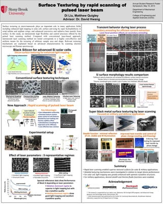
  • 1. Surface Texturing by rapid scanning of pulsed laser beam Di Liu, Matthew Quigley Advisor: Dr. David Hwang Annual Student Research Poster Symposium, May 10, 2013 Department of Mechanical Engineering College of Engineering and Applied Sciences (CEAS) Surface texturing in micro/nanoscale plays an important role in many application fields including enhanced light trapping in solar cell, surface anti-icing by super hydrophobicity in wind turbine and airplane wings, and enhanced convective and radiative heat transfer from surface. In this study, we demonstrate high flexibility and control precision offered by the pulsed laser scanning method. Compared with conventional laser-based approach, nanosecond laser scanning method we tested corresponds to a highly cost-effective and uniform means for the texturing of arbitrary sample area and shape. Relevant texturing mechanisms are explained based on advanced characterization by scanning electron microscope and Raman spectroscopy. Acknowledgement Summary • Rapid laser scanning enabled superior textured surfaces for solar & military applications. • Detailed texturing mechanisms were investigated in relation to target device performance. • For solar cell, light trapping was greatly enhanced with optimal crystalline structures. • For military applications, desired stealth and thermo-fluidic functions were enabled. *. The research is supported by Yuco optics corp. (Bohemia, NY) through SPIR program, and Advanced Energy Research and Technology Center (Stony Brook, NY). *. SEM characterization was performed at the Center for Functional Nanomaterials, Brookhaven National Laboratory supported by US Department of Energy. New Approach : Rapid scanning of pulsed laser beam Conventional surface texturing techniques By D. Neuhaus et al. (2007)By D. Yong Wu et al. (2007) By L. Dobrzaǹski et al. (2008) By SiOnyx Ti c-Si c-Si c-Si Chemical Wet Etching • Limited flexibility as crystalline plane dictates Laser Ablative Texturing • Loose structural: issues on carrier transport and limit in current extraction Ultrafast Laser Texturing • High laser cost, lack of arbitrary scale uniformity Mechanical Roughing • Quality limited due to friction with abrasive particles Experimental setup Effect of laser parameters : 3 representative regimes Ablation dominant • Excellent light trapping • Structural issues Melting dominant • Excellent light trapping • Favorable structures Mild melting • Insufficient light trapping • Low textures Spectral reflectance data show Performance of Black Si depending on laser parameters Silicon surface texturing for enhanced light trapping Si surface morphology results comparison *Different optical properties are achieved by different surface texture structures *Brown Silicon is formed and dominated by ablative phase change *Shorter wavelength gives smaller scale of spikes and shallower affected depth Brown Si Black Si λ=355nm Super black metal surface texturing by laser scanning Black Cu SEM image http://en.wikipedia.org/wiki/F-117_Nighthawk http://thegundeck.blogspot.com/2011/01/how- much-for-pentagon.html Black Silicon for advanced Si solar cells • Laser-based texturing • High flexibility and control precision Light trapping enhancement Stealth function : minimal reflection of UV, visible and IR illumination Enforcing Pool boiling for improved heat transfer by phase change http://www.81.net/hangkongdongtai/04262301 92013_3.html http://isnps.unm.edu/research/facilities/ IR image Cu Blackbody-like Thermal Emission Key Advantages • Size independent uniformity • Precision texture control: active control of unit features dictated by local melting and thermo-capillary effect • Simultaneous annealing for improved carrier diffusion • Cost-effective laser solution Photograph image SEM image • Ablation dominant regime is superior in light trapping but with low crystalline quality • Melting dominant regime show good light trapping and excellent crystalline quality Improved heat transfer and control of phase change (cooling, anti-freezing) Transient behavior during laser process Necessary ablation for spikes formation Secondary annealing for efficient current extraction On Laser focus Off Laser focus Laser focal position effects on secondary annealing Extended laser beam for annealing Cross section Raman spectroscopy Anti icing texturing Non-textured Textured http://www.gao.pitt.edu/antiicing.html 522cm-1 (Single crystal Si peak) Black Si λ=532nm Raman shift /cm-1 Efficient Current Extraction *Good Crystallinity *Minimal stress Focused on military and defense applications Black Cu Colorized Steel Reflect specific wavelength