
Recommended
More Related Content
What's hot
What's hot (20)
Viewers also liked
Similar to Bulk Micromachining Techniques for MEMS Components
Similar to Bulk Micromachining Techniques for MEMS Components (20)
More from Susovan Mondal
More from Susovan Mondal (7)
Recently uploaded
Recently uploaded (20)
Bulk Micromachining Techniques for MEMS Components
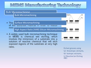
- 1. Bulk Micromachining This technique involves the selective removal of the substrate material in order to realize miniaturized mechanical components. A widely used bulk micromachining technique in MEMS is chemical wet etching, which involves the immersion of a substrate into a solution of reactive chemical that will etch exposed regions of the substrate at very high rates. Etched grooves using (a) Anisotropic etchants, (b) Isotropic etchants, (c) Reactive Ion Etching (RIE) Bulk Micromachining Surface Micromachining High Aspect Ratio (HAR) Silicon Micromachining
- 2. Surface Micromachining In surface micromachining, the MEMS sensors are formed on top of the wafer using deposited thin film materials. (a) Spacer layer deposition. (b) Pattering of the spacer layer. (c) Deposition of the microstructure layer. (d) Patterning of desired structure. (e) Stripping of the spacer layer resolves final structure.
- 3. High Aspect Ratio (HAR) Silicon Micromachining HAR combines aspects of both surface and bulk micromachining to allow for silicon structures with extremely high aspect ratios through thick layers of silicon (hundreds of nanometers, up to hundreds of micrometers). HAR MEMS technology enables a high degree of immunity to high-frequency, high-amplitude parasitic vibrations.