Metallic Thin Film Deposition for Sensing Applications

This poster presented the deposition of metallic thin film by the wet-chemistry methods, i.e. the galvanic displacement and the electrodeposition. The methods offered not only the simplicity and low-cost of the experimental setup, but also certain levels of control over the morphology, density, and size of the deposited metallic nanostructures. Several characterization methods were applied to examine the thin films, including the SEM, AFM, XRD, and XPS. Furthermore, thin film deposition by physical and chemical vapor deposition will be outlined for future work. Finally, the samples were tested for their applicability for Surface Enhanced Raman Spectroscopy (SERS) in which low concentrations of Rhodamine 6G (R6G) dye and paraoxon, a highly toxic organophosphate pesticide, were detected. They showed promising results.

Recommended
More Related Content
What's hot
What's hot (20)
Similar to Metallic Thin Film Deposition for Sensing Applications
Similar to Metallic Thin Film Deposition for Sensing Applications (20)
More from Minh Tran
More from Minh Tran (6)
Recently uploaded
Recently uploaded (20)
Metallic Thin Film Deposition for Sensing Applications
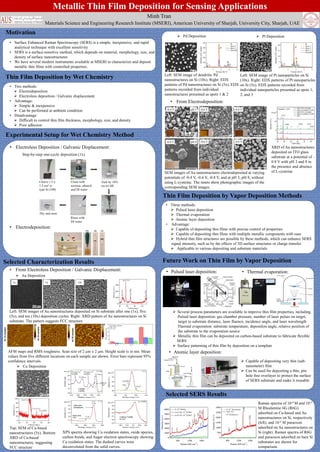
- 1. Metallic Thin Film Deposition for Sensing Applications Minh Tran Materials Science and Engineering Research Institute (MSERI), American University of Sharjah, University City, Sharjah, UAE Motivation • Surface Enhanced Raman Spectroscopy (SERS) is a simple, inexpensive, and rapid analytical technique with excellent sensitivity • SERS is a surface-sensitive method, which depends on material, morphology, size, and density of surface nanostructures • We have several modern instruments available at MSERI to characterize and deposit metallic thin films with controlled properties. Thin Film Deposition by Wet Chemistry • Two methods: Electrodeposition Electroless deposition / Galvanic displacement • Advantage: Simple & inexpensive Can be performed at ambient condition • Disadvantage: Difficult to control thin film thickness, morphology, size, and density Poor adhesion Experimental Setup for Wet Chemistry Method • Electrodeposition: • Electroless Deposition / Galvanic Displacement: Selected Characterization Results • From Electroless Deposition / Galvanic Displacement: Au Deposition Cu Deposition Pd Deposition Pt Deposition • From Electrodeposition: 1 μm Thin Film Deposition by Vapor Deposition Methods • Three methods: Pulsed laser deposition Thermal evaporation Atomic layer deposition • Advantage: Capable of depositing thin films with precise control of properties Capable of depositing thin films with multiple metallic components with ease Hybrid thin film structures are possible by these methods, which can enhance SERS signal intensity, such as by the effects of 3D surface structures or charge transfer. Applicable to various depositing and substrate materials Future Work on Thin Film by Vapor Deposition Several process parameters are available to improve thin film properties, including Pulsed laser deposition: gas chamber pressure, number of laser pulses on target, target to substrate distance, laser fluence, incidence angle, and laser wavelength Thermal evaporation: substrate temperature, deposition angle, relative position of the substrate to the evaporation source Metallic thin film can be deposited on carbon-based substrate to fabricate flexible SERS Surface patterning of thin film by deposition on a template • Pulsed laser deposition: • Thermal evaporation: • Atomic layer deposition: Capable of depositing very thin (sub- nanometer) film Can be used for depositing a thin, pin- hole free overlayer to protect the surface of SERS substrate and make it reusable Selected SERS Results Step-by-step one-cycle deposition (1x) Left: SEM images of Au nanostructures deposited on Si substrate after one (1x), five (5x), and ten (10x) deposition cycles. Right: XRD pattern of Au nanostructures on Si substrate. The pattern suggests FCC structure AFM maps and RMS roughness. Scan size of 2 μm x 2 μm. Height scale is in nm. Mean values from five different locations on each sample are shown. Error bars represent 95% confidence intervals. Top: SEM of Cu-based nanostructures (5x). Bottom: XRD of Cu-based nanostructures, suggesting FCC structure XPS spectra showing Cu oxidation states, oxide species, carbon bonds, and Auger electron spectroscopy showing Cu oxidation states. The dashed curves were deconvoluted from the solid curves. Left: SEM image of dendritic Pd nanostructures on Si (10x). Right: EDX patterns of Pd nanostructures on Si (5x). EDX patterns recorded from individual nanostructures presented as spots 1 & 2 Left: SEM image of Pt nanoparticles on Si (10x). Right: EDX patterns of Pt nanoparticles on Si (5x). EDX patterns recorded from individual nanoparticles presented as spots 1, 2, and 3 SEM images of Au nanostructures electrodeposited at varying potentials of -0.4 V, -0.6 V, -0.8 V, and at pH 3, pH 8, without using L-cysteine. The insets show photographic images of the corresponding SEM images. XRD of Au nanostructures deposited on ITO glass substrate at a potential of - 0.8 V with pH 3 and 8 in the presence and absence of L-cysteine Raman spectra of 10-4 M and 10-5 M Rhodamine 6G (R6G) adsorbed on Cu-based and Au nanostructures on Si, respectively (left), and 10-2 M paraoxon adsorbed on Au nanostructures on Si (right). Raman spectra of R6G and paraoxon adsorbed on bare Si substrates are shown for comparison.