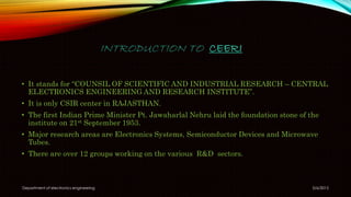
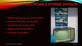
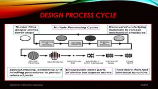
SUMMER TRAINING AT CSIR-CEERI
A presentation on
- A way to miniaturize our life style
IN
Submitted by :-
MANISH KUMAR KASWAN
B-tech Final year ECE
UCE, RTU, KOTA (Raj.)
INTRODUCTION TO CEERI
• It stands for “COUNSIL OF SCIENTIFIC AND INDUSTRIAL RESEARCH – CENTRAL
ELECTRONICS ENGINEERING AND RESEARCH INSTITUTE”.
• It is only CSIR center in RAJASTHAN.
• The first Indian Prime Minister Pt. Jawaharlal Nehru laid the foundation stone of the
institute on 21st September 1953.
• Major research areas are Electronics Systems, Semiconductor Devices and Microwave
Tubes.
• There are over 12 groups working on the various R&D sectors.
5/6/2015Department of electronics engineering
ELECTRONICS SYSTEMS DIVISION
5/6/2015Department of electronics engineering
• MEMS and Nano-sensors Group (MNG)
• Industrial Electronics Group (IEG)
• Agro Electronics Group (AEG)
• Digital System Group (DSG)
• IC Design Group (IDG)
WHAT IS MEMS ?
• Mems is a technology of very small devices. It is a combination of mechanical functions
and electrical functions on the same chip using micro fabrication technology.
• MEMS are made up of components between 1 to 100 micrometers in size
• MEMS devices generally range in size from 20 micrometers to a millimeter
5/6/2015Department of electronics engineering
Deposition Patterning Etching
Physical Chemical Lithography Dry Wet
Design process of mems
DEPOSITION
• Physical
 Physical vapor
deposition
 Electrodeposition
 Epatixial growth
 Thermal oxidation
• Chemical
 Chemical vapor
deposition
 Evaporation
 Sputtering
5/6/2015Department of electronics engineering
PATTERENING
Pattern Transfer
Alignment
Exposure
5/6/2015Department of electronics engineering
ETCHING
WET etching
This is the simplest etching
technology.
Wet etching works very well for
etching thin films on substrates.
It have two basic types
anisotropic and isotropic.
Dry etching
The dry etching technology can
split in three separate classes
called reactive ion etching (RIE),
sputter etching, and vapor phase
etching.
5/6/2015Department of electronics engineering
FABRICATION TECHNOLOGIES
• Ic fabrication technology
• Bulk Micromachining
• Surface Micromachining
• Micro molding
5/6/2015Department of electronics engineering
DESIGN PROCESS CYCLE
5/6/2015Department of electronics engineering
APPLICATIONS OF MEMS
In medicines In smartphones
In sensors In satalites
In automotives In boimems
As gyroscopes In military products 5/6/2015Department of electronics engineering
ADVANTAGES AND DISADVANTAGES
Advantages
Improved reproducibility.
Improved accuracy and reliability.
Increased selectivity and sensitivity.
Minimize energy and materials.
Disadvantages
 Farm establishment requires huge
investments.
 Micro-components are costly
compared to macro components.
 Design includes very much complex
procedures
5/6/2015Department of electronics engineering
VM-ADS
• Vehicle mounted-Active denial
systems
• This is an non-lethal, directed-
energy weapon.
• This is designed for area denial,
perimeter security and crowd
control.
• Still only U.S. army used it.
5/6/2015Department of electronics engineering
SMART SPOON
5/6/2015Department of electronics engineering
• The “smart” spoon allows
Parkinson’s sufferers to feed
themselves.
• It contains an ultra thin
rechargeable battery,
gyroscopes, motion-sensors and
actuators.
• It has multiple attachments for
different foods.
Conclusion
• This enabling technology
promises to create entirely new
categories of products.
• Mems will be the indispensible
factor in advancing technology
• As with all emerging technologies
had been predicted to
revolutionize technology and our
lives
5/6/2015Department of electronics engineering
REFERENCES
Online Resources
• IEEE Explore
http://ieeexplore.ieee.org/Xplore/Dyn
Wel.jsp
• MEMS Clearinghouse
http://www.memsnet.org/
• MOSIS http://www.mosis.org/
• Trimmer http://www.trimmer.net/
Journals
• •Journal of Micromechanical Systems .
• Journal of Micromechanics and
Microengineering.
• Sensors Magazine.
5/6/2015Department of electronics engineering
QUERIES???
5/6/2015Department of electronics engineering

Summer trainingin MEMS at CSIR-CEERI

  • 1.
    SUMMER TRAINING ATCSIR-CEERI A presentation on - A way to miniaturize our life style IN Submitted by :- MANISH KUMAR KASWAN B-tech Final year ECE UCE, RTU, KOTA (Raj.)
  • 2.
    INTRODUCTION TO CEERI •It stands for “COUNSIL OF SCIENTIFIC AND INDUSTRIAL RESEARCH – CENTRAL ELECTRONICS ENGINEERING AND RESEARCH INSTITUTE”. • It is only CSIR center in RAJASTHAN. • The first Indian Prime Minister Pt. Jawaharlal Nehru laid the foundation stone of the institute on 21st September 1953. • Major research areas are Electronics Systems, Semiconductor Devices and Microwave Tubes. • There are over 12 groups working on the various R&D sectors. 5/6/2015Department of electronics engineering
  • 3.
    ELECTRONICS SYSTEMS DIVISION 5/6/2015Departmentof electronics engineering • MEMS and Nano-sensors Group (MNG) • Industrial Electronics Group (IEG) • Agro Electronics Group (AEG) • Digital System Group (DSG) • IC Design Group (IDG)
  • 4.
    WHAT IS MEMS? • Mems is a technology of very small devices. It is a combination of mechanical functions and electrical functions on the same chip using micro fabrication technology. • MEMS are made up of components between 1 to 100 micrometers in size • MEMS devices generally range in size from 20 micrometers to a millimeter 5/6/2015Department of electronics engineering
  • 5.
    5/6/2015Department of electronicsengineering Deposition Patterning Etching Physical Chemical Lithography Dry Wet Design process of mems
  • 6.
    DEPOSITION • Physical  Physicalvapor deposition  Electrodeposition  Epatixial growth  Thermal oxidation • Chemical  Chemical vapor deposition  Evaporation  Sputtering 5/6/2015Department of electronics engineering
  • 7.
  • 8.
    ETCHING WET etching This isthe simplest etching technology. Wet etching works very well for etching thin films on substrates. It have two basic types anisotropic and isotropic. Dry etching The dry etching technology can split in three separate classes called reactive ion etching (RIE), sputter etching, and vapor phase etching. 5/6/2015Department of electronics engineering
  • 9.
    FABRICATION TECHNOLOGIES • Icfabrication technology • Bulk Micromachining • Surface Micromachining • Micro molding 5/6/2015Department of electronics engineering
  • 10.
    DESIGN PROCESS CYCLE 5/6/2015Departmentof electronics engineering
  • 11.
    APPLICATIONS OF MEMS Inmedicines In smartphones In sensors In satalites In automotives In boimems As gyroscopes In military products 5/6/2015Department of electronics engineering
  • 12.
    ADVANTAGES AND DISADVANTAGES Advantages Improvedreproducibility. Improved accuracy and reliability. Increased selectivity and sensitivity. Minimize energy and materials. Disadvantages  Farm establishment requires huge investments.  Micro-components are costly compared to macro components.  Design includes very much complex procedures 5/6/2015Department of electronics engineering
  • 13.
    VM-ADS • Vehicle mounted-Activedenial systems • This is an non-lethal, directed- energy weapon. • This is designed for area denial, perimeter security and crowd control. • Still only U.S. army used it. 5/6/2015Department of electronics engineering
  • 14.
    SMART SPOON 5/6/2015Department ofelectronics engineering • The “smart” spoon allows Parkinson’s sufferers to feed themselves. • It contains an ultra thin rechargeable battery, gyroscopes, motion-sensors and actuators. • It has multiple attachments for different foods.
  • 15.
    Conclusion • This enablingtechnology promises to create entirely new categories of products. • Mems will be the indispensible factor in advancing technology • As with all emerging technologies had been predicted to revolutionize technology and our lives 5/6/2015Department of electronics engineering
  • 16.
    REFERENCES Online Resources • IEEEExplore http://ieeexplore.ieee.org/Xplore/Dyn Wel.jsp • MEMS Clearinghouse http://www.memsnet.org/ • MOSIS http://www.mosis.org/ • Trimmer http://www.trimmer.net/ Journals • •Journal of Micromechanical Systems . • Journal of Micromechanics and Microengineering. • Sensors Magazine. 5/6/2015Department of electronics engineering
  • 17.
  • 18.