
Recommended
More Related Content
What's hot
What's hot (20)
Similar to Solutions manual for logic and computer design fundamentals 5th edition by mano ibsn 9780133760637
Similar to Solutions manual for logic and computer design fundamentals 5th edition by mano ibsn 9780133760637 (20)
Recently uploaded
Recently uploaded (20)
Solutions manual for logic and computer design fundamentals 5th edition by mano ibsn 9780133760637
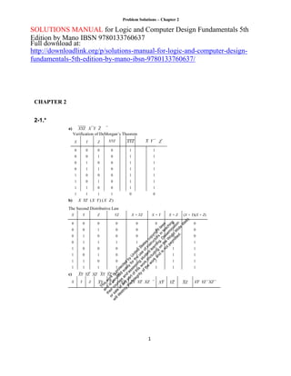
- 1. Problem Solutions – Chapter 2 1 X Y Z XYZ XYZ X Y 0 0 0 0 1 1 0 0 1 0 1 1 0 1 0 0 1 1 0 1 1 0 1 1 1 0 0 0 1 1 1 0 1 0 1 1 1 1 0 0 1 1 1 1 1 1 0 0 SOLUTIONS MANUAL for Logic and Computer Design Fundamentals 5th Edition by Mano IBSN 9780133760637 Full download at: http://downloadlink.org/p/solutions-manual-for-logic-and-computer-design- fundamentals-5th-edition-by-mano-ibsn-9780133760637/ CHAPTER 2 2-1.* a) XYZ X Y Z Verification of DeMorgan’s Theorem Z b) X YZ (X Y) (X Z) The Second Distributive Law X Y Z YZ X + YZ X + Y X + Z (X + Y)(X + Z) 0 0 0 0 1 1 1 1 0 0 1 1 0 0 1 1 0 1 0 1 0 1 0 1 0 0 0 1 0 0 0 1 0 0 0 1 1 1 1 1 0 0 1 1 1 1 1 1 0 1 0 1 1 1 1 1 0 0 0 1 1 1 1 1 c) XY YZ XZ XY YZ XZ X Y Z XY Y Z XZ XY YZ XZ XY YZ XZ XY YZ XZ
- 2. Problem Solutions – Chapter 2 2 0 0 0 0 1 1 1 1 0 0 1 1 0 0 1 1 0 1 0 1 0 1 0 1 0 0 1 1 0 0 0 0 0 1 0 0 0 1 0 0 0 0 0 0 1 0 1 0 0 1 1 1 1 1 1 0 0 0 0 0 1 1 0 0 0 0 1 0 0 0 1 0 0 1 0 1 0 0 0 0 0 1 1 1 1 1 1 0 2-2.* a) X Y XY XY = X Y (XY XY ) (XY XY) X (Y Y ) Y(X X ) X Y
- 3. Problem Solutions – Chapter 2 3 b) AB BC AB BC (AB AB) (BC BC) B(A A) B(C C) B B 1 c) Y XZ XY Y XY XZ (Y X )(Y Y ) XZ Y X XZ Y (X X )(X Z) X Y Z d) XY Y Z XZ XY YZ = 1 = X Y Z = XY XZ YZ XY YZ(X X ) XZ XY YZ XY XYZ XYZ XZ XY YZ XY (1 Z) XYZ XZ XY YZ XY XZ(1 Y ) XY YZ XY XZ XY(Z Z) YZ XY XZ XYZ YZ (1 X ) XY XZ(1 Y) YZ XY XZ YZ 2-3.+ a) ABC BCD BC CD = B CD ABC ABC BC BCD BCD CD AB(C C) BC(D D) BC CD AB BC BC CD B AB CD B CD b) WY WYZ WXZ WXY = WY WXZ XYZ XYZ (WY WXYZ ) (WXYZ WXYZ ) (WXYZ WXYZ) (WXYZ WXY Z) (WY WXYZ) (WXYZ WXY Z) (WXYZ WXYZ ) (WXYZ WXYZ) WY WXZ(Y Y ) XYZ (W W ) XYZ(W W ) WY WXZ XYZ XYZ c) AD AB CD BC = (A B C D)(A B C D) AD AB CD BC (A D)(A B)(C D)(B C) (AB AD BD)(BC BD CD) ABCD ABCD (A B C D)(A B C D) (A B C D)(A B C D)
- 4. Problem Solutions – Chapter 2 4 2-4.+ Given: A B 0, A B 1 Prove: (A C)(A B)(B C) (AB AC BC)(B C) AB AC BC 0 C(A B) C(A B)(0) C(A B)(A B) C(AB AB B BC = BC 2-5.+ Step 1: Define all elements of the algebra as four bit vectors such as A, B and C: A = (A3, A2, A1, A0) B = (B3, B2, B1, B0) C = (C3, C2, C1, C0) Step 2: Define OR1, AND1 and NOT1 so that they conform to the definitions of AND, OR and NOT presented in Table 2-1. a) A + B = C is defined such that for all i, i = 0, ... ,3, Ci equals the OR1 of Ai and Bi. b) A B = C is defined such that for all i, i = 0, ... ,3, Ci equals the AND1 of Ai and Bi. c) The element 0 is defined such that for A = “0”, for all i, i = 0, ... ,3, Ai equals logical 0. d) The element 1 is defined such that for A = “1”, for all i, i = 0, ... ,3, Ai equals logical 1. e) For any element A, A is defined such that for all i, i = 0, ... ,3, Ai equals the NOT1 of Ai. 2-6. a) AC ABC BC AC ABC (ABC BC) AC (ABC ABC BC (AC AC) BC A BC b) (A B C)(ABC) AABC ABBC ABCC (AA)BC A(BB)C AB(CC) ABC ABC ABC ABC c) ABC AC A(BC C) A(B C) d) ABD ACD BD (AB B AC)D (A AC B)D (A B)D e) (A B)(A C)(ABC) AAABC ACABC BAABC BCABC ABC
- 5. Problem Solutions – Chapter 2 5 2-7.* a) XY XYZ XY X XYZ (X XY )(X Z) (X X )(X Y )(X Z) (X Y )(X Z) X YZ b) X Y(Z X Z) X Y (Z XZ ) X Y (Z X )(Z Z) X YZ XY (X X )(X Y ) YZ X Y YZ X Y c) WX (Z YZ) X (W WYZ) WXZ WXYZ WX WXYZ WXZ WXZ WX WX WX X d) (AB AB)(CD CD) AC ABCD ABCD ABCD ABCD A C ABCD A C A C A(BCD) A C C(BD) A C BD 2-8. a) F ABC AC AB b) F ABC AC AB (A B C) (A C) (A B) (ABC)( AC)(AB) c) Same as part b. 2-9.* a) F (A B)( A B) b) F ((V W )X Y )Z c) F [W X (Y Z)(Y Z)][W X YZ YZ] d) F ABC (A B)C A(B C) 2-10.* Truth Tables a, b, c X Y Z a A B C b W X Y Z c 0 0 0 0 0 0 0 1 0 0 0 0 0 0 0 1 0 0 0 1 1 0 0 0 1 0 0 1 0 0 0 1 0 0 0 0 1 0 1 0 1 1 1 0 1 1 1 0 0 1 1 0 1 0 0 0 1 0 0 0 0 1 0 0 0 1 0 1 1 1 0 1 0 0 1 0 1 0 1 1 0 1 1 1 0 0 0 1 1 0 1 1 1 1 1 1 1 1 1 0 1 1 1 0 1 0 0 0 0 1 0 0 1 0 1 0 1 0 1 1 0 1 1 0 1 1 0 0 1 1 1 0 1 1 1 1 1 0 1 1 1 1 1 1
- 6. Problem Solutions – Chapter 2 6 a) Sum of Minterms: XYZ XYZ XYZ XYZ Product of Maxterms: (X Y Z)( X Y Z)(X Y Z)(X Y Z) b) Sum of Minterms: ABC ABC ABC ABC Product of Maxterms: (A B C)( A B C)( A B C)( A B C) c) Sum of Minterms: WXYZ WXYZ WXYZ WXY Z WXYZ WXYZ WXYZ Product of Maxterms: (W X Y Z)(W X Y Z)(W X Y Z) (W X Y Z)(W X Y Z)(W X Y Z) (W X Y Z)(W X Y Z)(W X Y Z) 2-11. a) E m(1, 2, 4, 6) M(0, 3, 5, 7), F m(0, 2, 4, 7) M(1, 3, 5, 6) b) E m(0, 3, 5, 7), F m(1, 3, 5, 6) c) E F m(0, 1, 2, 4, 6, 7), E F m(2, 4) d) E XYZ XYZ XY Z XYZ , F XY Z XYZ XY Z XYZ e) E Z(X Y ) XYZ, F Z(X Y ) XYZ 2-12.* a) (AB C)(B CD) AB ABCD BC AB BC s.o.p. B(A C) p.o.s. b) X X(X Y )(Y Z) (X X )(X (X Y )(Y Z)) (X X Y )(X Y Z) p.o.s. (1 Y )(X Y Z) X Y Z s.o.p. c) (A BC CD)(B EF) (A B C)( A B D)( A C D)(B EF ) (A B C)( A B D)( A C D)(B E)(B F) p.o.s. (A BC CD)(B EF ) A(B EF ) BC(B EF ) CD(B EF ) AB AEF BCEF BCD CDEF s.o.p. 2-13. a) A B b) c) B Y D C Z Y C A Z A C B X B W C D Y A B X C Z
- 7. Problem Solutions – Chapter 2 7 Y 1 1 X 1 1 Y 1 X 1 1 1 B 1 1 A 1 1 1 a) Y 1 1 X 1 1 b) B 1 1 1 1 A 1 B 1 1 1 A 1 1 1 C 1 1 1 1 1 1 A 1 1 D Y 1 1 1 1 X W 1 1 1 1 Z 2-14. a) b) c) d) B 1 1 1 A 1 1 1 C 1 Z XY +YZ+XYZ Z XY + XZ + YZ C C + AB AB + AC + BC or BC + AB + AC 2-15.* c) Z XZZ + XY C AA+CCB C BB+CC 2-16. a) b) c) C 1 1 1 1 B B A 1 1 1 1 D BD ABC ACD AC AD ABC X Z Y Z WX Y W XYZ 2-17. a) Y 1 1 1 1 1 X W 1 b) C 1 1 1 1 B A 1 1 1 1 1 1 1 Z D F XZ Y Z W XY W XYZ F BC ACD ABD ABC (ABD or ACD)
- 8. Problem Solutions – Chapter 2 8 b) Y 1 1 1 1 X W 1 1 1 1 Z c) C 1 1 1 1 B A 1 1 1 1 D Y 1 X 1 1 1 a) F Y 0 0 0 0 0 X W 0 0 0 Z b) F C 0 0 0 0 A 0 0 0 0 0 0 D m( m( m( 2-18.* a) Z m3 5 6 7 3, 5, 6, 7) m3 4 5 7 9 13 14 15 3, 4, 5, 7, 9, 13, 14, 15) m0 2 6 7 8 10 13 15 0, 2, 6, 7, 8, 10, 13, 15) 2-19.* a) Prime XZ, WX , XZ, WZ Essential XZ, XZ b) Prime CD, AC, BD, ABD, BC Essential AC, BD, ABD c) Prime AB, AC, AD, BC, BD, CD Essential AC, BC, BD 2-20. a) Prime BD, ACD, ABC, ABC, ACD b) Essential ACD, ABC, ABC, ACD Redundant BD F ACD ABC ABC ACD Prime WY, XY,WXZ ,W X , XYZ,WYZ Essential WY , XY Redundant W X , XYZ ,WYZ F WY XY WXZ c) Prime W Z, X Z,WYZ , XYZ ,W XY,W XZ,WXY Essential W Z, X Z Redundant =W XY,W XZ,WXY F W Z X Z WYZ XYZ 2-21. B F m(3, 4,5, 6,7,9,11,13) F m(0, 2, 6, 7, 8, 9, 10, 12, 14, 15) F W X WYZ XYZ F (W X )(W Y Z)(X Y Z) F BD BC ABC AD F (B D)(B C)(A B C)(A D) 2-22.* a) s.o.p. CD AC BD b) s.o.p. AC BD AD c) s.o.p. BD ABD (ABC or ACD) p.o.s. (C D)( A D)( A B C) p.o.s. (C D)( A D)( A B C) p.o.s. (A B)(B D)(B C D)
- 9. Problem Solutions – Chapter 2 9 1 1 1 X X 1 X X 1 X X 1 1 X 1 X B X 1 A 1 X 1 X X 1 X 1 1 1 1 X 1 X X DPrimesPri AmBe,s A=C,ABCA, CABBCC ABC PrimesPriXmZe,s X=Z,XWZXXYZ, WXXYY, WYXYZ, WWYYZZ WYZ PriPmreismesAB=, ACB, ACD,ABDDBD EssentEiaslsenAtBia,lA=C,ABBCAC BC F = AB + AC + BC F AB AC BC EssentEiaslsenXtZial = XZ F = XZ + WXY + WXY F XZ WXY WXY EssEesnstieanltiaCl ,=ADC AD F = C + AD + BD or AB F C AD( BD or AB) 2-26. a)(1) a)(2) Y b)(1) C b)(2) X X 0 X 0 1 X 0 0 1 1 0 X X 0 X B 2-23. a) s.o.p. ABD ABC ABD ABC b) s.o.p. X YZ W Z or ACD BCD ACD BCD p.o.s. (X Y Z)(W X Z) p.o.s. (A B D)( A B C)( A B D)( A B C) or (A C D)(B C D)( A C D)(B C D) 2-24. B A C C Y X 1 B X A 1 1 W X X X D Z F A C F AD (ABD BCD) or F XY ZW XY WYZ XYZ (ACD BCD) or (ABD ABC) 2-25.* a) b) Y 1 1 c) C 1 1 X X X 1 1 W A C 1 X Z X X 0 X Y X X 0 X C X X 0 X 0 1 0 1 X W 1 0 X X 0 1 0 1 X W 1 0 X X 0 1 X 0 B B A 0 1 1 0 A 0 X 1 X Z 0 X 1 X Z X X 0 X D D F WY Y Z WYZ WX Z F (XY or X Z) WYZ WY Z (WXZ or WYZ ) F ((X Y) or (X+Z))(W+Y+Z)(W+Y+Z) ((W+X+Z) or (W+Y+Z)) F BD F B D F BD
- 10. Problem Solutions – Chapter 2 10 2-27.* X Y XY XY Dual(X Y ) Dual( XY XY ) (X Y )(X Y ) XY XY XY XY X Y 2-28. ABCD AD AD ABCD (A D) Note that X Y (X Y ) XY Letting X ABCD and Y A D, We can observe from the map below or determine algebraically that XY is equal to 0. C 1 1 1 1 B A 1 1 1 1 1 D For this situation, X Y (X Y ) XY (X Y ) 0 X Y So, we can write F( A, B, C, D) X Y ABCD (A D) A B D C F 2-29.* The longest path is from input C or D. 0.073 ns + 0.073 ns + 0.048 ns + 0.073 ns = 0.267 ns
- 11. Problem Solutions – Chapter 2 11 2-30. a) b) c) 0 1.0 2.0 3.0 4.0 5.0 6.0 7.0 8.0 9.0 ns 2-31. a) tPHL-C, D to F 2tPLH 2 tPHL 2(0.36) 2(0.20) 1.12 ns tPLH-C, D to F 2tPHL 2tPLH 2(0.20) 2(0.36) 1.12 ns tpd 1.12 ns tPHL-B to F 2tPHL tPLH 2(0.20) (0.36) 0.76 ns tPLH-B to F 2tPHL tPLH 2(0.36) (0.20) 0.92 ns tpd-B to F 0.76 0.92 0.84 ns tPHL-A, B, C to F tPLH tPHL 0.36 0.20 0.56 ns t PLH-A, B, C to F t PHL t PLH 0.20 0.36 0.56 ns tpd-A, B, C to F 0.56 ns b) tpd-C, D to F 4 tpd 4(0.28) 1.12 ns tpd-B to F 3 tpd 3(0.28) 0.78 ns tpd-A, B, C to F 2 tpd 2(0.28) 0.56 ns c) For paths through an odd number of inverting gates with unequal gate tPHL and tPLH, path tPHL, tPLH, and tpd are different. For paths through an even number of inverting gates, path tPHL, tPLH, and tpd are equal. 2-32. If the rejection time for inertial delays is greater than the propagation delay, then an output change can occur before it can be predicted whether or not it is to occur due to the rejection time. For example, with a delay of 2 ns and a rejection time of 3 ns, for a 2.5 ns pulse, the initial edge will have already appeared at the output before the 3 ns has elapsed at which whether to reject or not is to be determined.
- 12. Problem Solutions – Chapter 2 11 predicts the follbut mo de ls the rej ctio n behav ior: : e is narrower than 0.05 ns, no output pulse occurs so the rejection time is 0.05 ns. The resulting model inaccurate for both 2-33.+ a) The propagation delay is tpd max(tPHL 0.05, tPLH 0.10) 0.10 ns. a) The propagation delay istpd = maxt(PHL = 0.05, tPLH = 0.10) = 0.10 ns. Assuming that tah)eTghaetepirsoapnaignavteiortnerd,efolaryaisptpodsi=tivemoauxttp(PuHtLp=ul0se.0,5th, etPfLoHllo=w0in.1g0a)ct=ua0ll.y10ocncsur.s: Assuming that the gate is an inv, efrotrera positiv e output pulse, the f ollowing actually occurs: Assuming that the gate is an inv, efrotrera positiv e output pulse, the f ollowing actually occurs: 0.05 ns 0.10 ns0.05 ns 0.10 ns If the input pulse is narrower than 0.05 ns, no output pulse occurs so the rejection time is 0.05 ns. If the input pulsTIfhethreesinupltuint gpum lsoedeisl pnraerdroicwtes rtthheanf o0ll.o0w5inngs,rensoulot su,tpwuhticpfhuelrsdefifromccuthrse saocttuha el dree jlea cytiob nehtai,mveioris 0.05 ns. The resulting model predicts the f ollowing results, whicfherdfifrom the actual delay beha,v iorowing results, which differ from the actual delay behavior, but models the rejection behavior: : but models the rejection behav ior: : 0.10 ns 0.10 ns0.10 ns 0.10 ns b) For a negative output pulse, the following actually occurs: b) For a negative output pulse,the following actually occurs: b) For a negative output pulse,the following actually occurs: 0.05 ns 0.15 ns 0.050n.1s0 ns 0.15 ns 0.10 ns The model predicts the behavior: The model predicts the f ollowing results, whicfhedrsif f rom the actual delay behav ior and f rom following results, which differs from the actual delay behavior and from the actual rejection Tthe amctoudael rlepjerecdtiiocntsbetheavfioll:owing results, whicfhedrsif f rom the actual delay behav ior and f rom the actual rejection behavior: 0.10 ns0.10 ns Overall, the model is 0.10 ns0.10 ns casesaand b,and providesafaulty rejection Omvoedraelll,fthoer mcaosdeelbis. inUacsciunrgataenfoarvbeortahPgcHeaLsoeafsnatdaPtnLdH bf,oarnptdd pwrovildeismapfraouvltey rtehjecdtieolnay Overall, the model is inacmaccuocrdautereal fcfoyororbfcotathhsecemasboe.sdeaUlafnosdrincbgi,rcaaunnditapavrpoepvrliacdgaetseioaonaffsan,utdbltutytrtehjfeocrrteiotjencwmtiooudlemdl foimodrepclraosstveillebf.atihlUse.sdineglaaynPHL PLH pd average of tPHL and tPLH foacrctpudrawcoyuoldf tihmepmroovedethl efodreclairycuaictcauprapcliycaotfiothnes,mbuodt ethl feorrecjeircctuioitnamppolidcealtisotnilsl,fabiulst.the rejection model still fails. 2-34.* X1 N1 N2 X2 N3 N4 X3 N5 X4 N6 f 2-35. -- Figure 4-40: Structural VHDL Description library ieee; use ieee.std_logic_1164.all; entity nand2 is port(in1, in2: in std_logic; out1 : out std_logic); end nand2;
- 13. Problem Solutions – Chapter 2 12 0 2 1 2 architecture concurrent of nand2 is begin out1 <= not (in1 and in2); end architecture; library ieee; use ieee.std_logic_1164.all; entity nand3 is port(in1, in2, in3 : in std_logic; out1 : out std_logic); end nand3; architecture concurrent of nand3 is begin out1 <= not (in1 and in2 and in3); end concurrent; library ieee; use ieee.std_logic_1164.all; entity nand4 is port(in1, in2, in3, in4: in std_logic; out1 : out std_logic); end nand4; -- The code above this point could be eliminated by using the library, func_prims. library ieee; use ieee.std_logic_1164.all; entity fig440 is port(X: in std_logic_vector(2 to 0); f: out std_logic); end fig440; architecture structural_2 of fig440 is component NAND2 port(in1, in2: in std_logic; out1: out std_logic); end component; component NAND3 port(in1, in2, in3: in std_logic; out1: out std_logic); end component; signal T: std_logic_vector(0 to 4); begin g0: NAND2 port map (X(2),X(1),T(0)); g1: NAND2 port map (X(2),T(0),T(1)); g2: NAND2 port map (X(1),T(0),T(2)); g3: NAND3 port map (X(1),T(1),T(2),T(3)); g4: NAND2 port map (X(1),T(2),T(4)); g5: NAND2 port map (T(3),T(4),f); end structural_2; F =X X + X X F X X X X0 2 1 0
- 14. Problem Solutions – Chapter 2 13 tura _1; f 2-36.begin g0: bNeOgTin_1 port map (D, x1); X= D + BC Y= A BCD g1: ANDg_02:pNoOrt mT_ap1(pBo, rCt,mx2a);p (D, x1); X D BC g2: NOR g_ 12 :p Ao Nrt m Da _p 2(A po, x r1 t, mx3 a) p; (B, C, x2); Y ABCD g3: NANgD2_:2NpOorRt m_2app(ox1rt, xm3,axp4)(;A, x1, x3); g4: OR_g23p:oNrt AmNapD(x_12, xp2o,rxt5m); ap (x1, x3, x4); g5: ANDg_42:pOoRrt m_2appo(xr4t, mx5a, pX)(;x1, x2, x5); g6: ANDg_52:pAoNrt mDa_p2(xp3o,rxt5m, Ya)p; (x4, x5, X); end struc g6:l AND_2 port map (x3, x5, Y); end structural_1; 2-37. a b a c b c b g a c d 2-38.* begin F <= (X and Z) or ((not Y) and Z); end; 2-39.* X1 N1 N2 X2 N3 N4 X3 N5 X4 N6 f
- 15. Problem Solutions – Chapter 2 14 2-40. module circuit_4_50(A, B, C, D, X, Y); input A, B, C, D; output X, Y; wire n1, n2, n3, n4, n5; not go(n1, D); nand g1(n4, n1, n3); and g2(n2, B, C), g3(X, n4, n5), g4(Y, n3, n5); or g5(n5, n1, n2); nor g6(n3, n1, A); endmodule
- 16. Problem Solutions – Chapter 2 15 g T 4],X[2],T[2]), f 2-41. module circuit_4_51(X, F); module circuiit_n4p_u5t1[(2X:,0F]);X; input [2:0o]uXt;put F; output F; wire [0:4]wTi;re [0:4] T; nand nand g0(T[0],X[0],X[1]), g0(T[0],X[0],X[1]), g1(Tg[1],TX[01]],,TX[0[]0),],T[0]), g2(Tg[2],TX[12]],,TX[0[]1),],T[0]), g3(Tg[3],TX[23]],,TX[1[]2,T],[T2][)1, ],T[2]), g4(T[4],X[2],T[2]), g5(,FT[3],T[4]); endmodule g5(F,T[3],T[4]); endmodule 2-42. a b a c b c b g a c d 2-43.* module circuit_4_53(X, Y, Z, F); input X, Y, Z; output F; assign F = (X & Z) | (Z & ~Y); endmodule SOLUTIONS MANUAL for Logic and Computer Design Fundamentals 5th Edition by Mano IBSN 9780133760637 Full download at: http://downloadlink.org/p/solutions-manual-for-logic-and-computer- design-fundamentals-5th-edition-by-mano-ibsn-9780133760637/ People also search: logic and computer design fundamentals 5th edition solutions logic and computer design fundamentals 5th edition chegg logic and computer design fundamentals 3rd edition pdf logic and computer design fundamentals 2nd edition pdf digital logic and computer design
- 17. Problem Solutions – Chapter 2 16 logic and comput er design fundam entals ppt logic and comput er design fundam entals compa nion website logic and comput er design fundam entals table of content s