SlideShare a Scribd company logo
1 of 7
Download to read offline
designfeature By Mike Stein, Paradigm Works

AS DIGITAL DESIGN BECOMES INCREASINGLY SOPHISTICATED,
CIRCUITS WITH MULTIPLE CLOCKS MUST RELIABLY
COMMUNICATE WITH EACH OTHER.


Crossing the abyss:
asynchronous signals
in a synchronous world
      nly the most elementary logic circuits use a           ogy, operating conditions, and the load on the out-

O     single clock. Most data-movement applica-
      tions, including disk-drive controllers, CD-
ROM/DVD controllers, modems, network inter-
                                                             put for outputs that are not buffered. Sharp edge
                                                             rates on the input signal minimize the window. More
                                                             windows of vulnerability arise as the clock frequen-
faces, and network processors, bear inherent                 cy increases, and the probability of hitting the win-
challenges moving data across multiple clock do-             dow increases as the data frequency increases.
mains. When signals travel from one clock domain                FPGA manufacturers and IC foundries qualify
to another, the signal appears to be asynchronous            their flip-flops and determine their characteristics.
in the new clock domain.                                     “MTBF” (mean time between failures) describes the
   In modern IC, ASIC, and FPGA designs, engineers           metastability characteristic of a flip-flop using sta-
have many software programs to help them create              tistics to determine the probability of a flip-flop’s
million-gate circuits, but these programs do not             failure. Manufacturers base the MTBF in part on the
solve the problem of signal synchronization. It is up        length of the time window during which a change in
to the designer to know reliable design techniques           the input signal causes the flip-flop to become un-
that reduce the risk of failure for circuits commu-          stable. In addition, MTBF calculation uses the fre-
nicating across clock domains.                               quency of the input signal and the frequency of the
                                                             clock driving the flip-flop.
FUNDAMENTALS                                                    Each type of flip-flop in an ASIC or FPGA library
   The first step in managing multiclock designs is          has timing requirements to help you determine the
to understand the problem of signal stability. When          window of vulnerability. “Setup time” describes the
a signal crosses a clock domain, it appears to the cir-      time an input signal to a flip-flop must be stable be-
cuitry in the new clock domain as an asynchronous            fore the clock edge. “Hold time” is the time the sig-
signal. The circuit that receives this signal needs to       nal must remain stable after the clock edge. These
synchronize it. Synchronization prevents the meta-           specifications are usually conservative to account for
stable state of the first storage element (flip-flop) in     all the possible variations in supply voltage, operat-
the new clock domain from propagating through the
circuit.                                                                                         NO COMBINATIONAL LOGIC HERE

   Metastability is the inability of a flip-flop to arrive            CLOCK 1 DOMAIN                   CLOCK 2 DOMAIN

at a known state in a specific amount of time. When
                                                                DATA         D SET Q            D SET Q              D SET Q    OUTPUT
a flip-flop enters a metastable state, you can predict
neither the element’s output voltage level nor when
                                                                                CLR Q               CLR Q               CLR Q
the output will settle to a correct voltage level. Dur-
ing this settling time, the flip-flop’s output is at some     CLOCK 1          CLOCK 2
intermediate voltage level or may oscillate and can
cascade the invalid output level to flip-flops                          In a full synchronizer circuit, the signal-cross-
                                                          Figure 1
farther down the signal path.                                           ing clock domains should pass from the origi-
   The input must be stable during a small window nating flip-flop in the original clock domain to the first flip-
of time around the active edge of the clock for any flop of the synchronizer without passing through any combi-
flip-flop. This window of time is a function of the national logic between the originating flip-flop and the first
design of the flip-flop, the implementation technol- flip-flop of the synchronizer.
www.edn.com                                                                                                          July 24, 2003 | edn 59
designfeature Asynchronous signals

ing temperature, signal quality, and fab-                                     BASIC SYNCHRONIZER
                                                                                                                                A
rication. If a design meets these timing                                                                                        B
                                                                                                                                          OUTPUT
                                                        DATA                 D SET Q          D SET Q             D SET Q
requirements, the possibility is negligible
that the flip-flop will fail.
                                                                               CLR Q              CLR Q             CLR Q
   Synthesis programs in modern IC and
FPGA designs ensure that digital circuits         CLOCK 2                                                                               Figure 2
meet the setup-and-hold requirements
for each flip-flop in the design; however,       The edge-detecting synchronizer circuit adds a flip-flop to the output of the level synchronizer.
asynchronous signals pose problems for
the software. A signal crossing a clock do-      job by placing the flip-flops close to each              cles in the new clock domain. A require-
main appears to be asynchronous to the           other and preventing you from placing                    ment of this circuit is that the signal
logic in the new clock domain. Most syn-         any combinational logic between them.                    needs to change to its invalid state before
thesis programs have trouble determin-              For synchronization to work properly,                 it can become valid again. Each time the
ing whether asynchronous signals meet            the signal crossing a clock domain should                signal goes valid, the receiving logic con-
the timing requirements for flip-flops.          pass from flip-flop in the original clock                siders it a single event, no matter how
Because they cannot determine the time           domain to the first flip-flop of the syn-                long the signal remains valid. This circuit
the flip-flop is unstable, they cannot de-       chronizer without passing through any                    is the heart of all other synchronizers.
termine the total delay from the flip-flop       combinational logic between the two                         The edge-detecting synchronizer cir-
through the combinational logic to the           (Figure 1). This requirement is important                cuit adds a flip-flop to the output of the
next flip-flop. The best course, then, is to     because the first stage of a synchronizer is             level synchronizer (Figure 2). The output
use circuits that mitigate the impact of         sensitive to glitches that combination log-              of the additional flip-flop is inverted and
asynchronous signaling.                          ic produces. A long enough glitch that oc-               ANDed with the output of the level syn-
                                                 curs at the correct time could meet the                  chronizer. This circuit detects the rising
SIGNAL SYNCHRONIZATION                           setup-and-hold requirements of the first                 edge of the input to the synchronizer and
   The purpose of synchronizing signals          flip-flop in the synchronizer, leading the               generates a clockwide, active-high pulse.
is to protect downstream logic from the          synchronizer to pass a false-valid indica-               Switching the inverter on the AND gate
metastable state of the first flip-flop in a     tion to the rest of the logic in the new                 inputs creates a synchronizer that detects
new clock domain. A simple synchroniz-           clock domain.                                            the falling edge of the input signal.
er comprises two flip-flops in series with-         A synchronized signal is valid in the                 Changing the AND gate to a NAND gate
out any combinational circuitry between          new clock domain after two clock edges.                  results in a circuit that generates an ac-
them. This design ensures that the first         The signal delay is between one and two                  tive-low pulse.
flip-flop exits its metastable state and its     clock periods in the new clock domain. A                    The edge-detecting synchronizer works
output settles before the second flip-flop       rule of thumb is that a synchronizer cir-                well at synchronizing a pulse going to a
samples it. You also need to place the flip-     cuit causes two clock cycles of delay in the             faster clock domain. This circuit produces
flops close to each other to ensure the          new clock domain, and a designer needs                   a pulse that indicates the rising or falling
smallest possible clock skew between             to consider how synchronization delay                    edge of the input signal. One restriction
them.                                            impacts timing of signals crossing clock                 of this synchronizer is that the width of
   IC foundries help with signal synchro-        domains.                                                 the input pulse must be greater than the
nization by providing synchronizer cells.           There are many designs for synchro-                   period of the synchronizer clock plus the
These cells usually comprise a flip-flop         nizers because one type does not work                    required hold time of the first synchro-
with a very high gain that uses more pow-        well in all applications. Synchronizers fall             nizer flip-flop. The safest pulse width is
er and is larger than a standard flip-flop.      into one of three basic categories: level,               twice the synchronizer clock period. This
Such a flip-flop has reduced setup-and-          edge-detecting, and pulse (Table 1). Oth-                synchronizer does not work if the input is
hold-time requirements for the input sig-        er synchronizer designs exist, but these                 a single clockwide pulse entering a slow-
nal and is resistant to oscillation when the     serve for most applications a designer en-               er clock domain; however, the pulse syn-
input signal causes a metastable condi-          counters. In a level synchronizer, the sig-              chronizer solves this problem.
tion. Another type of synchronizer cell          nal crossing a clock domain stays high                      The input signal of a pulse synchro-
contains two flip-flops, thus easing your        and stays low for more than two clock cy-                nizer is a single clockwide pulse that trig-
                                                                                                          gers a toggle circuit in the originating
 TABLE 1—SYNCHRONIZER TYPES AND USES                                                                      clock domain (Figure 3). The output of
 Type        Application             Input      Output         Restriction                                the toggle circuit switches from high to
 Level       Synchronizes level      Level      Level          Input must be valid for at least two       low and vice versa each time it receives a
 signals                                                       clock periods in the new domain.           pulse and passes through the level syn-
                                                               Each time output goes valid counts         chronizer to arrive at one input of the
                                                                as a single event.                        XOR gate, while a one-clock-cycle-de-
 Edge-       Detects rising or       Level or   Pulse          Input must be valid for at least two       layed version goes to the other input of
 detecting   falling edge of input   pulse                     clock periods in the new domain.           the XOR. For one clock cycle, each time
 Pulse       Synchronizes single     Pulse      Pulse          Input pulses must have at least two        the toggle circuit changes state, the out-
             clockwide pulses                                  clock periods between them in the          put of this synchronizer generates a sin-
                                                               new domain.                                gle clockwide pulse.
60 edn | July 24, 2003                                                                                                                   www.edn.com
designfeature Asynchronous signals
                                                              TOGGLE CIRCUIT
                                                              (CLOCK 1 DOMAIN)


                                                                              BASIC SYNCHRONIZER
                                                                                                                                          A
                       0                                TOGGLE                                                                                         OUTPUT
                                        D SET Q                              D SET Q              D SET Q               D SET Q           B
                       1

   DATA                                    CLR Q                               CLR Q                CLR Q                  CLR Q
                                                                                                                                                      Figure 3
 CLOCK 1                                         CLOCK 2


The input signal of a pulse synchronizer is a single-clock, cyclewide pulse that triggers a toggle circuit in the originating clock domain.

   The basic function of a pulse synchro- cate with each other when the response                    Full- and partial-handshake signaling
nizer is to take a single clockwide pulse time of one or both circuits is unpre- are the two fundamental types of hand-
from one clock domain and create a sin- dictable. For example, an arbitrated bus shake protocol that circuits on different
gle clockwide pulse in the new domain. allows more than one circuit to request clock domains use. Each type of hand-
One restriction of a pulse synchronizer is access to a single bus, such as PCI or shake uses synchronizers, and each has its
that input pulses must have a minimum AMBA (Advanced Microcontroller Bus own set of design trade-offs. In full-hand-
spacing between pulses equal to two syn- Architecture), using arbitration to deter- shake signaling, the two circuits wait for
chronizer clock periods. If the input puls- mine which circuit gains access to the bus. each other before asserting or dropping
es are closer, the output pulses in the new Each circuit signals a request, and the ar- their respective handshake signal (Figure
clock domain are adjacent to each other, bitration logic determines which request 4). First, Circuit A asserts its request sig-
resulting in an output pulse that is wider “wins.” This winning circuit receives an nal. Next, Circuit B detects that the request
than one clock cycle. This problem is more acknowledgment indicating that it has signal is valid and asserts its acknowledg-
severe when the clock period of input access to the bus. It then discontinues its ment signal. When Circuit A detects that
pulse is greater than twice the synchro- request and begins the bus transaction.                 the acknowledgment signal is valid, it
nizer clock period. In this case,                                                                           drops its request signal. Finally,
if the input pulses are too close,                                                                          when Circuit B detects that the
                                          CIRCUIT A
the synchronizer does not detect (CLOCK DOMAIN A) 1           ASSE
                                                                   RT RE                                    request is invalid, it drops its ac-
                                                                          QUES             CIRCUIT B
every one.                                                                     T                            knowledgment signal. Circuit A
                                                                                       (CLOCK DOMAIN B)
                                                                                      2 TWO CLOCKS          does not make a new request
HANDSHAKING AND FIFOs                                                                 3 ONE CLOCK           until it detects that the ac-
   In many applications, simple                                                  DGE                        knowledgment signal is invalid.
                                                                             WLE
                                                                       C KNO
signals are not the only infor-            TWO CLOCKS 4           RT A                                         This type of handshake uses
                                                             ASSE
                                                              DEAS
mation crossing clock domains;              ONE CLOCK 5            SERT
                                                                          REQU                              level synchronizers. A designer
                                                                               EST
data, address, and con-                                                                                     uses this technique when the
                              Figure 4                                               6 TWO CLOCKS
trol buses also travel                                                                                      acknowledging circuit (Circuit
                                                                                     7 ONE CLOCK
together across domains. Engi-                                                                              B) needs to inform the re-
                                                                                EDGE
neers have at their disposal ad-                                            OWL                             questing circuit (Circuit A)
                                                                     ACKN
                                                                SERT
ditional tools, such as hand-              TWO CLOCKS 8    DEAS                                             that it is actively processing the
shaking protocols and FIFOs,            TOTAL: FIVE CLOCKS                           TOTAL: SIX CLOCKS      request. This handshake re-
that can handle these situations.                                                                           quires that the requesting cir-
   Handshaking allows digital In full-handshake signaling, the two circuits wait for each other            cuit hold off its next request
circuits to effectively communi- before asserting or dropping their respective handshake signals.          until it detects that the ac-

 TABLE 2—HANDSHAKING TECHNIQUES
 Handshake type       Circuits         Signaling type      Sequence length       Synchronizer        Restrictions

 Full                 Circuit A        Level               Five clocks           Level               Sequence is long.
                      (request)                                                                      Request must be invalid for at least two of the Circuit B
                                                                                                     clock periods.
                      Circuit B        Level               Six clocks            Level               Acknowledgment must be invalid for at least two of the
                      (acknowledge)                                                                  Circuit A clock periods.
 Partial I            Circuit A        Level               Three clocks          Pulse or edge-      Must control rate of acknowledgment pulses.
                      (request)                                                  detect
                      Circuit B        Pulse               Five clocks           Level               Request must be invalid for at least two of the Circuit B
                      (acknowledge)                                                                  clock periods.
 Partial II           Circuit A        Pulse               Two clocks            Pulse or edge-      Must save pending request information.
                      (request)                                                  detect
                      Circuit B        Pulse               Three clocks          Pulse or edge-      Must register request and acknowledgment signals.
                      (acknowledge)                                              detect


62 edn | July 24, 2003                                                                                                                               www.edn.com
designfeature Asynchronous signals

knowledgment signal is invalid.                                                                                  full handshake signaling. You
                                           CIRCUIT A
To determine the timing for this (CLOCK DOMAIN A) 1              ASSE
                                                                       RT RE                   CIRCUIT B         can shave off a few more clock
                                                                             QUES          (CLOCK DOMAIN B)
protocol, use the rules of thumb                                                  T                              cycles using a second partial-
that signals take two clock cy-                                                            2 TWO CLOCKS          handshake scheme where Cir-
cles to cross a clock domain and                                                           3  ONE CLOCK          cuit A asserts its request with a
that circuits register signals be-                                            O WLE
                                                                                    DGE                          single clockwide pulse and Cir-
                                                                          CKN
fore they cross clock domains.             TWO CLOCKS 4              RT A                                        cuit B acknowledges the request
                                                               ASSE
The complete sequence takes a               ONE CLOCK 5           DEAS                                           with a single clockwide pulse.
                                                                        SERT
                                                                              REQU
                                                                                    EST
maximum of five cycles in the A                                                                                  In this case, both circuits need
clock domain plus a maximum                                                                6 TWO CLOCKS          to save state to indicate that the
of six cycles in the B clock                                                                                     request is pending.
domain. Full handshak-             Figure 5                                                                         This type of handshake uses
ing is robust because each                                                                                       pulse synchronizers, but either
circuit explicitly knows the state TOTAL: THREE CLOCKS                                     TOTAL: FIVE CLOCKS    circuit that has a clock that is
of the other by examining the                                                                                    twice as fast as the other can in-
request and acknowledgment In a partial-handshake scheme, Circuit A asserts its request signal,                  stead use an edge-detecting syn-
signals. The drawback of this and Circuit B acknowledges it with a single clockwide pulse.                       chronizer instead (Figure 6).
scheme is that the entire                                                                                        The complete sequence takes a
process uses many clock cycles                                                                                  maximum of two cycles in the A
                                          CIRCUIT A    1       ASSE
to complete the transaction.          (CLOCK DOMAIN A)
                                                                    RT RE
                                                                           QUES
                                                                                T
                                                                                              CIRCUIT B         clock domain plus a maximum
                                                                                          (CLOCK DOMAIN B)
   Partial handshaking is an-                                                                                   of three cycles in the B clock do-
                                                                                         2 TWO CLOCKS
other signaling technique that                                                                                  main. This partial-handshaking
                                                                                         3 ONE CLOCK
shortens this sequence of                                                                                       technique uses three fewer clock
events. With partial handshake                                            NOW
                                                                              LEDG
                                                                                   E                            cycles in the A clock domain and
                                           TWO CLOCKS 4                CK
signaling, the two circuits com-                                  RT A                                          three fewer clock cycle in the B
                                                             ASSE
municating with each other do                                                                                   clock domain than full-hand-
not wait for the other one                                                                                      shake signaling. This technique
before dropping their re-         Figure 6                                                                      is also faster than the first par-
spective signal and continuing                                                                                  tial-handshake signaling by one
with the handshake sequence.                                                                                    cycle in the A clock domain and
Partial handshaking is less ro-                                                                                 two cycles in the B clock domain
                                        TOTAL: TWO CLOCKS                               TOTAL: THREE CLOCKS
bust than full handshaking be-                                                                                  (Table 2). These handshake pro-
cause the handshake signals do This type of partial-handshake scheme uses pulse synchronizers, but              tocols involve single signals that
not indicate the state of both a circuit that has a clock that is twice as fast as the other can instead        cross clock domains. However,
circuits; each circuit must save use an edge-detecting synchronizer.                                            when groups of signals cross
state information normally                                                                                      clock domains, designers need to
present in full handshake signals. How- one clock cycle; otherwise, Circuit B can- use more complex signaling schemes.
ever, by not waiting until the other circuit not distinguish between a previous re-
drops it handshake signal, the whole se- quest and a new request. With this hand- DATAPATH DESIGN
quence of events takes less time.                 shake, Circuit B uses a level synchronizer              One important rule when synchroniz-
   When using partial-handshake signal- for the request signal, and Circuit A uses ing signals is that a design should not
ing, the acknowledging circuit must gen- a pulse synchronizer for the acknowl- synchronize the same signal in more than
erate its signal at the correct time. If the edgment signal. The acknowledgment one place; that is, a single signal fans out
acknowledging circuit needs to complete pulses occur only when Circuit B detects to more than one synchronizer. Because
processing the request before it can han- the request signal. This situation allows synchronization takes one to two clock
dle another, then the timing of the ac- Circuit A to control the spacing of puls- cycles, a designer cannot reliably predict
knowledgment signal is important. The es it receives into the synchronizer by when each of these signals arrives across
circuit uses its acknowledgment signal to controlling the timing of its request sig- a clock domain. In addition, the timing
indicate when it completed any process- nal (Figure 5). Once again, to determine of a group of synchronized signals in the
ing. One partial-handshake scheme mix- timing, use the rules of thumb that sig- new clock domain can vary because the
es level and pulse signaling, and the oth- nals take two clock cycles to cross a clock delay can be either a single clock cycle of
er uses only pulse signaling.                     domain and that circuits register signals delay or two cycles, depending on when
   In the first partial-handshake scheme, before they cross clock domains.                             the input arrives at the synchronizer. This
Circuit A asserts its request signal as an           The complete sequence takes a maxi- situation results in a “race condition” be-
active level, and Circuit B acknowledges mum of three cycles in the A clock do- tween the individually synchronized sig-
it with a single clockwide pulse. In this main plus a maximum of five cycles in nals. This race condition also applies to
case, Circuit B does not care when Cir- the B clock domain. This partial hand- groups of signals, such as data, address,
cuit A drops its request signal. However, shake signaling uses two fewer clock cy- and control buses, that need to travel to-
to make this technique work, Circuit A cles in the A clock domain and one few- gether across clock domains. Thus, you
must drop its request signal for at least er clock cycle in the B clock domain than should not use individual synchronizers
64 edn | July 24, 2003                                                                                                               www.edn.com
designfeature Asynchronous signals

                         on each signal in the
                         group or on each bit                                      REQUEST
                                                                                               SYNCHRONIZE
                         of a data bus or an ad-
                         dress bus in which                     SYNCHRONIZE
                                                                                ACKNOWLEDGE
                         each signal
                         needs to be          Figure 7
                         valid in the new clock           CIRCUIT A                                    CIRCUIT B
                                                                     HOLD           DATA      SAMPLE
                         domains at the same
                         time.
                            One way to solve A datapath-synchronizer design uses a holding register and hand-
                         the problem of bus shake signaling.
                         synchronization is to
                         use a holding register and handshake sig- sends it. These situations call for the use
                         naling. This circuit comprises a register of a FIFO.
                         that holds the signal bus and a hand-               Fundamentally, a designer uses a FIFO
                         shaking scheme (Figure 7). The hand- for speed matching, data-width match-
                         shake signals indicate when the circuit in ing, or both. For speed matching, the
                         the new clock domain can sample the bus faster port on the FIFO handles burst
                         and when the originating circuit can re- transfers while the slower port handles
                         place the current contents of the hold- constant rate transfers. However, even
                         ing register.                                    with different access types and speeds,
                            In this design, the transmitting circuit the average data rates into and out of the
                         stores the data (signal bus) in the hold- FIFO have to be the same; otherwise, the
                         ing register as it asserts the request signal. FIFO overflows or underflows. Like the
                         These two actions can happen at once be- single-register design, the FIFO holds
                         cause the request signal takes at least one data in registers or memory while it syn-
                         clock cycle before the receiving circuit de- chronizes status signals that determine
                         tects it (the minimum handshake-syn- when data can be written into the FIFO
                         chronization delay). When the receiving or when data can be read out of it.
                         circuit samples the data (signal bus), it as-       In speed-matching applications, each
                         serts the acknowledgment signal. This de- port (read or write) has a different clock.
                         sign uses full handshaking and takes a The registers in the FIFO use the write-
                         long time to complete the transfer. A de- port clock, just as the holding register uses
                         sign using full-handshake signaling has a the clock of the circuit changing the reg-
                         large window of time for the receiving cir- ister’s contents. Signal synchronization
                         cuit to sample the signal bus and is thus takes place in the pointer logic and is
                         somewhat inefficient. The same design more complex than handshake signaling.
                         can use a partial handshake instead of a            Several approaches exist for designing
                         full handshake to speed the transfer.            the pointer logic. The first method is to
                            With this type of bus synchronization, synchronize the read and write strobes
                         you synchronize the handshake signals while using counters in each clock do-
                         but not the signal bus. The signal bus main to track the available entries in the
                         originates from the holding register and FIFO. The counters reflect the number of
                         remains stable until after the receiving FIFO entries available for reading or
                         circuit samples it. Note that bus syn- writing, and the counters are synchro-
                         chronization may not work in applica- nous with their respective ports. The read
                         tions in which the transmitting circuit counter tracks the number of entries that
                         presents data too fast for the receiving contain valid data, and the write count-
                         circuit to handle it.                            er tracks the number of entries available
                                                                          to store data. When you reset the point-
                         ADVANCED DATAPATH DESIGN                         er logic, the read counter starts at zero
                            In many cases, data needs to “pile up” because no data is available to read. The
                         as it crosses clock domains, so designs us- write counter starts at the number of en-
                         ing a single holding register do not work. tries in the FIFO, meaning that all the en-
                         One such case is a transmitting circuit tries are available for storing data.
                         that presents data in bursts, too quickly           The read strobe decrements the read
                         for a receiving circuit to sample. Anoth- counter and is synchronized to the write-
                         er such case is a receiving circuit that clock domain before it increments the
                         samples data faster, but in a narrower write counter. The write strobe decre-
                         data width, than the transmitting circuit ments the write counter and is synchro-
66 edn | July 24, 2003                                                                                www.edn.com
designfeature Asynchronous signals
                                                                                                       BINARY ADDER
                         nized to the read-clock domain before it
                         increments the read counter.                     GRAY CODE
                                                                          TO BINARY
                            This design requires single clockwide                                         BINARY TO
                                                                                                          GRAY CODE
                         pulses and pulse synchronizers for the
                         read and write strobes because, as a level                     1
                         signal crosses from one clock domain to
                         a faster one, it remains valid for more           POINTER
                                                                         (GRAY CODE)
                         clock cycles in the faster domain than in
                         the slow one. Because each counter                            The Gray-code counter, a bina-
                                                                     Figure 8
                         changes whenever the read or write                            ry adder, has converters from
                         signal is valid, then the faster clock do- and to Gray code before and after the adder.
                         main detects more reads or writes than
                         actually occurred in the slower clock do- triggers, you must set the empty status to
                         main. Pulse synchronizers translate a give the read circuitry time to prevent a
                         clockwide pulse in one clock domain to read of an empty FIFO.
                         a clockwide pulse in the new clock do-           This pointer logic restricts circuits
                         main, and each pulse represents one read from accessing the FIFO on every clock
                         or write of the FIFO.                         cycle, even in the slow clock domain. The
                            This FIFO-status technique gives pes- advantage of this feature is that the cir-
                         simistic status for both reads and writes. cuits accessing the FIFO have at least one
                         The status for the write port indicates full clock cycle to evaluate the FIFO status.
                         when the FIFO has all entries filled and The FIFO can have every entry filled with
                         continues to indicate full after the read data without overwriting valid data or
                         strobe triggers, because synchronization can be empty without reading invalid
                         delays the strobe to the write counter. data. Another advantage of this design is
                         This situation is also true for the empty that each side can read its respective
                         status on the read port, because syn- counter and determine how many entries
                         chronization delays the write strobe to are available. A designer can use this FIFO
                         the read counter.                             design for circuits that perform multiple
                            Another consideration for this design reads or writes of data without causing an
                         is detecting full or empty at the right underflow or overflow condition.
                         time. If the FIFO has one entry remain-          The drawback of this design is that
                         ing, and the write strobe triggers, the counters, rather than direct comparisons
                         FIFO must then set the full status. This of the read and write pointers, determine
                         scenario gives the full indication one status. For large FIFOs, these counters are
                         clock sooner to allow the circuit writing large. Also, the average data rates are half
                         into the FIFO enough time to stop the the slowest clock frequency, because the
                         next write from overflowing the FIFO. read or write pulses from the faster clock
                         This situation is also true for the read domain must have at least two clock pe-
                         port of the FIFO. In this case, if the FIFO riods between them in the slow-clock do-
                         has only one entry, and the read strobe main when using pulse synchronizers.
                                                                       One way to eliminate some of these
                          TABLE 3—GRAY CODE VERSUS problems is to use direct pointer com-
                                                                       parison.
                                     BINARY CODE                          In this FIFO design, comparing the
                            Decimal         Binary           Gray      read and write pointers determines the
                               0                0               0      FIFO status. Pointer comparison in asyn-
                               1                1               1
                               2               10              11
                                                                       chronous designs is more challenging,
                               3               11              10      because each pointer exists in a different
                               4              100             110      clock domain, and synchronizing a sig-
                               5              101             111      nal bus requires that the bus does not
                               6              110             101      change while synchronizing handshake
                               7              111             100      signals. A FIFO design using this tech-
                               8             1000            1100
                                                                       nique for pointer synchronization would
                               9             1001            1101
                               10            1010            1111
                                                                       be slow. To solve this problem, the FIFO
                               11            1011            1110      pointer logic uses Gray code instead of
                               12            1100            1010      binary code for the pointers.
                               13            1101            1011         Gray code changes only one bit at a
                               14            1110            1001      time for each increase or decrease in the
                               15            1111            1000      count (Table 3). You can use synchroniz-
68 edn | July 29, 2003                                                                                  www.edn.com
ers on Gray-code buses because only one          nals that cross clock domains from caus-
signal changes each time the bus changes,        ing unpredictable behavior in circuits, use
eliminating the race condition between           synchronization. Level synchronizers
bits of the Gray-coded bus as it passes          work well for signals that remain valid for
through separate synchronizers. The              many clock cycles. Use an edge-detecting
pointers for this design are Gray-code           synchronizer for level signals in the slow-
counters. Using binary pointers would re-        er clock domain that change to pulses in
quire synchronizing pointer values after         the new clock domain. Finally, use pulse
converting them to Gray code, and using          synchronizers for pulses crossing clock
conversion logic violates the restriction        domains. Remember that, when a signal
that synchronized signals originate from         bus crosses clock domains, it needs to ar-
flip-flops before crossing a clock domain.       rive in the new clock domain during the
   The Gray-code counter is a binary             same clock cycle. Do not synchronize each
adder with converters from and to Gray           signal but use a holding register and
code before and after the adder (Figure          handshaking. Handshaking indicates
8). Converting to and from Gray code is          when signals in the holding register are
an XOR operation, so you need only a few         valid and when to sample them. Using
more levels of logic than a binary count-        handshaking and a holding register is use-
er. To convert Gray code to binary, use:         ful for data buses but does not provide for
B N G N;      BN 1 BN GN 1;BN 2                  passing more than one data word at a time
BN 1 GN 2...B1 B2 G1; B0 B1 G0.                  to the new clock domain.
To convert binary to Gray code, use:
G N B N;      GN 1 BN BN 1;GN 2                  References
BN 1 BN 2...G1 B2 B1; G0 B1 B0.                     1. Davis, Leroy, Logic Metastability,
A design can use the same technique to           www.interfacebus.com/Design_MetaSta
compare Gray-code pointer values by              ble.html, September 2002.
adding converters between the pointers              2. Seed, Luke, Introduction to VLSI/
and binary-comparison logic.                     Clocked CMOS Circuits, The University of
   A FIFO with this pointer logic is fast,       Sheffield, UK, www.shef.ac.uk/eee/
and circuits can read or write the FIFO          teach/resources/eee310/documents/VLSI
on every clock cycle. However, accessing         _Clocked_CMOS.pdf, February 2002.
the FIFO on every cycle means the FIFO              3. Haseloff, Eilhard, “Metastable Re-
status has to include almost-full and al-        sponse in 5-V Logic Circuits,” Texas In-
most-empty indications, so that the cir-         struments Application Note SDYA006,
cuits accessing the FIFO have time to            www-s.ti.com/sc/psheets/sdya006/
stop. Almost full indicates that one entry       sdya006.pdf, February 1997.
is available to write, and almost empty             4. Cummings, Clifford E, “Synthesis
indicates that one entry remains unread.         and Scripting Techniques for Designing
This situation describes a design that           Multi-Asynchronous Clock Designs,”
needs the fewest possible status signals,        Synopsys Users Group Conference, San
and a design needs more indicators if the        Jose, CA, www.sunburst-design.com/pa-
circuits accessing the FIFO use a burst ac-      pers, March 2001.
cess with a fixed minimum size.                     5. “A Metastability Primer,” Philips
   This FIFO-status technique gives pes-         Semiconductors Application Note AN2-
simistic status for both reads and writes.       19, www.semiconductors.philips.com/
The status on the write port indicates full      acrobat/applicationnotes/AN219_1.
when the FIFO fills and continues to in-         pdf, Nov 15, 1989.
dicate full after it the circuit reads it, be-      6. Wakerly, John F, Digital Design: Prin-
cause synchronization delays the read            ciples and Practices, Prentice Hall, 1990.
pointer to the write-side comparison log-
ic. This situation is also true for the emp-     Author’s bio graphy
ty status on the read side, because syn-         Mike Stein is principal consulting engineer
chronization delays the write pointer to         at Paradigm Works (Andover, MA), where
the read-side comparison logic.                  he works on ASIC and FPGA design, syn-
   Handling signals crossing clock do-           thesis, and static-timing analysis. He re-
mains becomes less challenging when you          ceived a BSEE from Northeastern Univer-
design with techniques that reduce the           sity in 1995. His spare-time interests
risk of communication failure between            include playing video games with his son,
circuits in different domains. To prevent        photography, snowboarding, biking, and
metastability of flip-flops receiving sig-       building Lego robots.
www.edn.com                                                                                     July 24, 2003 | edn 69

More Related Content

What's hot

counter using 4 master slave flip-flops
counter using 4 master slave flip-flops counter using 4 master slave flip-flops
counter using 4 master slave flip-flops ZunAib Ali
 
14827 unit 4_clocked_flip_flops
14827 unit 4_clocked_flip_flops14827 unit 4_clocked_flip_flops
14827 unit 4_clocked_flip_flopsSandeep Kumar
 
Topic 3 Digital Technique Flip flop
Topic 3 Digital Technique Flip flopTopic 3 Digital Technique Flip flop
Topic 3 Digital Technique Flip flopBai Haqi
 
flip flop circuits and its applications
flip flop circuits and its applicationsflip flop circuits and its applications
flip flop circuits and its applicationsGaditek
 
sequential circuits
  sequential circuits  sequential circuits
sequential circuitssawsanalraisi
 
CSA Application of Flip Flop
CSA Application of Flip FlopCSA Application of Flip Flop
CSA Application of Flip FlopLansKaba
 
Sequential Circuits - Flip Flops (Part 2)
Sequential Circuits - Flip Flops (Part 2)Sequential Circuits - Flip Flops (Part 2)
Sequential Circuits - Flip Flops (Part 2)Abhilash Nair
 
Introduction to instruction set. new course
Introduction to instruction set. new courseIntroduction to instruction set. new course
Introduction to instruction set. new courseSamee Ur Rehman
 
B sc3 unit 5 sequencial lc
B sc3 unit 5 sequencial lcB sc3 unit 5 sequencial lc
B sc3 unit 5 sequencial lcMahiboobAliMulla
 
Hardware combinational
Hardware combinationalHardware combinational
Hardware combinationalDefri Tan
 
IS 151 Lecture 11
IS 151 Lecture 11IS 151 Lecture 11
IS 151 Lecture 11wajanga
 
DETECTION OF PHASE REVERSAL AND SINGLE PHASING OF AC POWER SUPPLY WITH D FLIP...
DETECTION OF PHASE REVERSAL AND SINGLE PHASING OF AC POWER SUPPLY WITH D FLIP...DETECTION OF PHASE REVERSAL AND SINGLE PHASING OF AC POWER SUPPLY WITH D FLIP...
DETECTION OF PHASE REVERSAL AND SINGLE PHASING OF AC POWER SUPPLY WITH D FLIP...saanavi
 
Divide by N clock
Divide by N clockDivide by N clock
Divide by N clockMantra VLSI
 
Sequential Logic Circuit
Sequential Logic CircuitSequential Logic Circuit
Sequential Logic CircuitRamasubbu .P
 

What's hot (20)

counter using 4 master slave flip-flops
counter using 4 master slave flip-flops counter using 4 master slave flip-flops
counter using 4 master slave flip-flops
 
14827 unit 4_clocked_flip_flops
14827 unit 4_clocked_flip_flops14827 unit 4_clocked_flip_flops
14827 unit 4_clocked_flip_flops
 
Jk flip flop
Jk flip flopJk flip flop
Jk flip flop
 
Topic 3 Digital Technique Flip flop
Topic 3 Digital Technique Flip flopTopic 3 Digital Technique Flip flop
Topic 3 Digital Technique Flip flop
 
flip flop circuits and its applications
flip flop circuits and its applicationsflip flop circuits and its applications
flip flop circuits and its applications
 
sequential circuits
  sequential circuits  sequential circuits
sequential circuits
 
Lecture 1 6844
Lecture 1 6844Lecture 1 6844
Lecture 1 6844
 
CSA Application of Flip Flop
CSA Application of Flip FlopCSA Application of Flip Flop
CSA Application of Flip Flop
 
Sequential circuits
Sequential circuitsSequential circuits
Sequential circuits
 
Presentation On Flip-Flop
Presentation On Flip-FlopPresentation On Flip-Flop
Presentation On Flip-Flop
 
Sequential Circuits - Flip Flops (Part 2)
Sequential Circuits - Flip Flops (Part 2)Sequential Circuits - Flip Flops (Part 2)
Sequential Circuits - Flip Flops (Part 2)
 
Introduction to instruction set. new course
Introduction to instruction set. new courseIntroduction to instruction set. new course
Introduction to instruction set. new course
 
B sc3 unit 5 sequencial lc
B sc3 unit 5 sequencial lcB sc3 unit 5 sequencial lc
B sc3 unit 5 sequencial lc
 
Hardware combinational
Hardware combinationalHardware combinational
Hardware combinational
 
IS 151 Lecture 11
IS 151 Lecture 11IS 151 Lecture 11
IS 151 Lecture 11
 
Cable
CableCable
Cable
 
Group 9 flip flops
Group 9 flip flopsGroup 9 flip flops
Group 9 flip flops
 
DETECTION OF PHASE REVERSAL AND SINGLE PHASING OF AC POWER SUPPLY WITH D FLIP...
DETECTION OF PHASE REVERSAL AND SINGLE PHASING OF AC POWER SUPPLY WITH D FLIP...DETECTION OF PHASE REVERSAL AND SINGLE PHASING OF AC POWER SUPPLY WITH D FLIP...
DETECTION OF PHASE REVERSAL AND SINGLE PHASING OF AC POWER SUPPLY WITH D FLIP...
 
Divide by N clock
Divide by N clockDivide by N clock
Divide by N clock
 
Sequential Logic Circuit
Sequential Logic CircuitSequential Logic Circuit
Sequential Logic Circuit
 

Similar to A sync in_sync

lecture-18.pptx
lecture-18.pptxlecture-18.pptx
lecture-18.pptxthunder_x
 
Design of -- Two phase non overlapping low frequency clock generator using Ca...
Design of -- Two phase non overlapping low frequency clock generator using Ca...Design of -- Two phase non overlapping low frequency clock generator using Ca...
Design of -- Two phase non overlapping low frequency clock generator using Ca...Prashantkumar R
 
Low power electronic design
Low power electronic designLow power electronic design
Low power electronic designMahesh Dananjaya
 
International Journal of Computational Engineering Research(IJCER)
International Journal of Computational Engineering Research(IJCER)International Journal of Computational Engineering Research(IJCER)
International Journal of Computational Engineering Research(IJCER)ijceronline
 
slides-main.pdf
slides-main.pdfslides-main.pdf
slides-main.pdfMatupi1
 
Design and implementation of qpsk modulator using digital subcarrier
Design and implementation of qpsk modulator using digital subcarrierDesign and implementation of qpsk modulator using digital subcarrier
Design and implementation of qpsk modulator using digital subcarrierGongadi Nagaraju
 
4 U 5 Slides With Notes
4 U 5 Slides With Notes4 U 5 Slides With Notes
4 U 5 Slides With Notesrameraja
 
VLSI Design Sequential circuit design
VLSI Design Sequential circuit designVLSI Design Sequential circuit design
VLSI Design Sequential circuit designtamil arasan
 
555 timer lab projects
555 timer lab projects555 timer lab projects
555 timer lab projectsBien Morfe
 
Iaetsd an mtcmos technique for optimizing low
Iaetsd an mtcmos technique for optimizing lowIaetsd an mtcmos technique for optimizing low
Iaetsd an mtcmos technique for optimizing lowIaetsd Iaetsd
 
Lecture intro to_wcdma
Lecture intro to_wcdmaLecture intro to_wcdma
Lecture intro to_wcdmaGurpreet Singh
 
Circuit Level Modelling Simulink Projects Research Help
Circuit Level Modelling Simulink Projects Research HelpCircuit Level Modelling Simulink Projects Research Help
Circuit Level Modelling Simulink Projects Research HelpMatlab Simulation
 

Similar to A sync in_sync (20)

lecture-18.pptx
lecture-18.pptxlecture-18.pptx
lecture-18.pptx
 
Design of -- Two phase non overlapping low frequency clock generator using Ca...
Design of -- Two phase non overlapping low frequency clock generator using Ca...Design of -- Two phase non overlapping low frequency clock generator using Ca...
Design of -- Two phase non overlapping low frequency clock generator using Ca...
 
Low Power VLSI Designs
Low Power VLSI DesignsLow Power VLSI Designs
Low Power VLSI Designs
 
Flip Flops
Flip FlopsFlip Flops
Flip Flops
 
VLSI Power in a Nutshell
VLSI Power in a NutshellVLSI Power in a Nutshell
VLSI Power in a Nutshell
 
Low power electronic design
Low power electronic designLow power electronic design
Low power electronic design
 
Low Power VLSI Design
Low Power VLSI DesignLow Power VLSI Design
Low Power VLSI Design
 
DLD Chapter-5.pdf
DLD Chapter-5.pdfDLD Chapter-5.pdf
DLD Chapter-5.pdf
 
International Journal of Computational Engineering Research(IJCER)
International Journal of Computational Engineering Research(IJCER)International Journal of Computational Engineering Research(IJCER)
International Journal of Computational Engineering Research(IJCER)
 
slides-main.pdf
slides-main.pdfslides-main.pdf
slides-main.pdf
 
Intro
IntroIntro
Intro
 
Design and implementation of qpsk modulator using digital subcarrier
Design and implementation of qpsk modulator using digital subcarrierDesign and implementation of qpsk modulator using digital subcarrier
Design and implementation of qpsk modulator using digital subcarrier
 
4 U 5 Slides With Notes
4 U 5 Slides With Notes4 U 5 Slides With Notes
4 U 5 Slides With Notes
 
Ofdm.pptx
Ofdm.pptxOfdm.pptx
Ofdm.pptx
 
VLSI Design Sequential circuit design
VLSI Design Sequential circuit designVLSI Design Sequential circuit design
VLSI Design Sequential circuit design
 
555 timer lab projects
555 timer lab projects555 timer lab projects
555 timer lab projects
 
Iaetsd an mtcmos technique for optimizing low
Iaetsd an mtcmos technique for optimizing lowIaetsd an mtcmos technique for optimizing low
Iaetsd an mtcmos technique for optimizing low
 
Lecture intro to_wcdma
Lecture intro to_wcdmaLecture intro to_wcdma
Lecture intro to_wcdma
 
Circuit Level Modelling Simulink Projects Research Help
Circuit Level Modelling Simulink Projects Research HelpCircuit Level Modelling Simulink Projects Research Help
Circuit Level Modelling Simulink Projects Research Help
 
Dx33746752
Dx33746752Dx33746752
Dx33746752
 

A sync in_sync

  • 1. designfeature By Mike Stein, Paradigm Works AS DIGITAL DESIGN BECOMES INCREASINGLY SOPHISTICATED, CIRCUITS WITH MULTIPLE CLOCKS MUST RELIABLY COMMUNICATE WITH EACH OTHER. Crossing the abyss: asynchronous signals in a synchronous world nly the most elementary logic circuits use a ogy, operating conditions, and the load on the out- O single clock. Most data-movement applica- tions, including disk-drive controllers, CD- ROM/DVD controllers, modems, network inter- put for outputs that are not buffered. Sharp edge rates on the input signal minimize the window. More windows of vulnerability arise as the clock frequen- faces, and network processors, bear inherent cy increases, and the probability of hitting the win- challenges moving data across multiple clock do- dow increases as the data frequency increases. mains. When signals travel from one clock domain FPGA manufacturers and IC foundries qualify to another, the signal appears to be asynchronous their flip-flops and determine their characteristics. in the new clock domain. “MTBF” (mean time between failures) describes the In modern IC, ASIC, and FPGA designs, engineers metastability characteristic of a flip-flop using sta- have many software programs to help them create tistics to determine the probability of a flip-flop’s million-gate circuits, but these programs do not failure. Manufacturers base the MTBF in part on the solve the problem of signal synchronization. It is up length of the time window during which a change in to the designer to know reliable design techniques the input signal causes the flip-flop to become un- that reduce the risk of failure for circuits commu- stable. In addition, MTBF calculation uses the fre- nicating across clock domains. quency of the input signal and the frequency of the clock driving the flip-flop. FUNDAMENTALS Each type of flip-flop in an ASIC or FPGA library The first step in managing multiclock designs is has timing requirements to help you determine the to understand the problem of signal stability. When window of vulnerability. “Setup time” describes the a signal crosses a clock domain, it appears to the cir- time an input signal to a flip-flop must be stable be- cuitry in the new clock domain as an asynchronous fore the clock edge. “Hold time” is the time the sig- signal. The circuit that receives this signal needs to nal must remain stable after the clock edge. These synchronize it. Synchronization prevents the meta- specifications are usually conservative to account for stable state of the first storage element (flip-flop) in all the possible variations in supply voltage, operat- the new clock domain from propagating through the circuit. NO COMBINATIONAL LOGIC HERE Metastability is the inability of a flip-flop to arrive CLOCK 1 DOMAIN CLOCK 2 DOMAIN at a known state in a specific amount of time. When DATA D SET Q D SET Q D SET Q OUTPUT a flip-flop enters a metastable state, you can predict neither the element’s output voltage level nor when CLR Q CLR Q CLR Q the output will settle to a correct voltage level. Dur- ing this settling time, the flip-flop’s output is at some CLOCK 1 CLOCK 2 intermediate voltage level or may oscillate and can cascade the invalid output level to flip-flops In a full synchronizer circuit, the signal-cross- Figure 1 farther down the signal path. ing clock domains should pass from the origi- The input must be stable during a small window nating flip-flop in the original clock domain to the first flip- of time around the active edge of the clock for any flop of the synchronizer without passing through any combi- flip-flop. This window of time is a function of the national logic between the originating flip-flop and the first design of the flip-flop, the implementation technol- flip-flop of the synchronizer. www.edn.com July 24, 2003 | edn 59
  • 2. designfeature Asynchronous signals ing temperature, signal quality, and fab- BASIC SYNCHRONIZER A rication. If a design meets these timing B OUTPUT DATA D SET Q D SET Q D SET Q requirements, the possibility is negligible that the flip-flop will fail. CLR Q CLR Q CLR Q Synthesis programs in modern IC and FPGA designs ensure that digital circuits CLOCK 2 Figure 2 meet the setup-and-hold requirements for each flip-flop in the design; however, The edge-detecting synchronizer circuit adds a flip-flop to the output of the level synchronizer. asynchronous signals pose problems for the software. A signal crossing a clock do- job by placing the flip-flops close to each cles in the new clock domain. A require- main appears to be asynchronous to the other and preventing you from placing ment of this circuit is that the signal logic in the new clock domain. Most syn- any combinational logic between them. needs to change to its invalid state before thesis programs have trouble determin- For synchronization to work properly, it can become valid again. Each time the ing whether asynchronous signals meet the signal crossing a clock domain should signal goes valid, the receiving logic con- the timing requirements for flip-flops. pass from flip-flop in the original clock siders it a single event, no matter how Because they cannot determine the time domain to the first flip-flop of the syn- long the signal remains valid. This circuit the flip-flop is unstable, they cannot de- chronizer without passing through any is the heart of all other synchronizers. termine the total delay from the flip-flop combinational logic between the two The edge-detecting synchronizer cir- through the combinational logic to the (Figure 1). This requirement is important cuit adds a flip-flop to the output of the next flip-flop. The best course, then, is to because the first stage of a synchronizer is level synchronizer (Figure 2). The output use circuits that mitigate the impact of sensitive to glitches that combination log- of the additional flip-flop is inverted and asynchronous signaling. ic produces. A long enough glitch that oc- ANDed with the output of the level syn- curs at the correct time could meet the chronizer. This circuit detects the rising SIGNAL SYNCHRONIZATION setup-and-hold requirements of the first edge of the input to the synchronizer and The purpose of synchronizing signals flip-flop in the synchronizer, leading the generates a clockwide, active-high pulse. is to protect downstream logic from the synchronizer to pass a false-valid indica- Switching the inverter on the AND gate metastable state of the first flip-flop in a tion to the rest of the logic in the new inputs creates a synchronizer that detects new clock domain. A simple synchroniz- clock domain. the falling edge of the input signal. er comprises two flip-flops in series with- A synchronized signal is valid in the Changing the AND gate to a NAND gate out any combinational circuitry between new clock domain after two clock edges. results in a circuit that generates an ac- them. This design ensures that the first The signal delay is between one and two tive-low pulse. flip-flop exits its metastable state and its clock periods in the new clock domain. A The edge-detecting synchronizer works output settles before the second flip-flop rule of thumb is that a synchronizer cir- well at synchronizing a pulse going to a samples it. You also need to place the flip- cuit causes two clock cycles of delay in the faster clock domain. This circuit produces flops close to each other to ensure the new clock domain, and a designer needs a pulse that indicates the rising or falling smallest possible clock skew between to consider how synchronization delay edge of the input signal. One restriction them. impacts timing of signals crossing clock of this synchronizer is that the width of IC foundries help with signal synchro- domains. the input pulse must be greater than the nization by providing synchronizer cells. There are many designs for synchro- period of the synchronizer clock plus the These cells usually comprise a flip-flop nizers because one type does not work required hold time of the first synchro- with a very high gain that uses more pow- well in all applications. Synchronizers fall nizer flip-flop. The safest pulse width is er and is larger than a standard flip-flop. into one of three basic categories: level, twice the synchronizer clock period. This Such a flip-flop has reduced setup-and- edge-detecting, and pulse (Table 1). Oth- synchronizer does not work if the input is hold-time requirements for the input sig- er synchronizer designs exist, but these a single clockwide pulse entering a slow- nal and is resistant to oscillation when the serve for most applications a designer en- er clock domain; however, the pulse syn- input signal causes a metastable condi- counters. In a level synchronizer, the sig- chronizer solves this problem. tion. Another type of synchronizer cell nal crossing a clock domain stays high The input signal of a pulse synchro- contains two flip-flops, thus easing your and stays low for more than two clock cy- nizer is a single clockwide pulse that trig- gers a toggle circuit in the originating TABLE 1—SYNCHRONIZER TYPES AND USES clock domain (Figure 3). The output of Type Application Input Output Restriction the toggle circuit switches from high to Level Synchronizes level Level Level Input must be valid for at least two low and vice versa each time it receives a signals clock periods in the new domain. pulse and passes through the level syn- Each time output goes valid counts chronizer to arrive at one input of the as a single event. XOR gate, while a one-clock-cycle-de- Edge- Detects rising or Level or Pulse Input must be valid for at least two layed version goes to the other input of detecting falling edge of input pulse clock periods in the new domain. the XOR. For one clock cycle, each time Pulse Synchronizes single Pulse Pulse Input pulses must have at least two the toggle circuit changes state, the out- clockwide pulses clock periods between them in the put of this synchronizer generates a sin- new domain. gle clockwide pulse. 60 edn | July 24, 2003 www.edn.com
  • 3. designfeature Asynchronous signals TOGGLE CIRCUIT (CLOCK 1 DOMAIN) BASIC SYNCHRONIZER A 0 TOGGLE OUTPUT D SET Q D SET Q D SET Q D SET Q B 1 DATA CLR Q CLR Q CLR Q CLR Q Figure 3 CLOCK 1 CLOCK 2 The input signal of a pulse synchronizer is a single-clock, cyclewide pulse that triggers a toggle circuit in the originating clock domain. The basic function of a pulse synchro- cate with each other when the response Full- and partial-handshake signaling nizer is to take a single clockwide pulse time of one or both circuits is unpre- are the two fundamental types of hand- from one clock domain and create a sin- dictable. For example, an arbitrated bus shake protocol that circuits on different gle clockwide pulse in the new domain. allows more than one circuit to request clock domains use. Each type of hand- One restriction of a pulse synchronizer is access to a single bus, such as PCI or shake uses synchronizers, and each has its that input pulses must have a minimum AMBA (Advanced Microcontroller Bus own set of design trade-offs. In full-hand- spacing between pulses equal to two syn- Architecture), using arbitration to deter- shake signaling, the two circuits wait for chronizer clock periods. If the input puls- mine which circuit gains access to the bus. each other before asserting or dropping es are closer, the output pulses in the new Each circuit signals a request, and the ar- their respective handshake signal (Figure clock domain are adjacent to each other, bitration logic determines which request 4). First, Circuit A asserts its request sig- resulting in an output pulse that is wider “wins.” This winning circuit receives an nal. Next, Circuit B detects that the request than one clock cycle. This problem is more acknowledgment indicating that it has signal is valid and asserts its acknowledg- severe when the clock period of input access to the bus. It then discontinues its ment signal. When Circuit A detects that pulse is greater than twice the synchro- request and begins the bus transaction. the acknowledgment signal is valid, it nizer clock period. In this case, drops its request signal. Finally, if the input pulses are too close, when Circuit B detects that the CIRCUIT A the synchronizer does not detect (CLOCK DOMAIN A) 1 ASSE RT RE request is invalid, it drops its ac- QUES CIRCUIT B every one. T knowledgment signal. Circuit A (CLOCK DOMAIN B) 2 TWO CLOCKS does not make a new request HANDSHAKING AND FIFOs 3 ONE CLOCK until it detects that the ac- In many applications, simple DGE knowledgment signal is invalid. WLE C KNO signals are not the only infor- TWO CLOCKS 4 RT A This type of handshake uses ASSE DEAS mation crossing clock domains; ONE CLOCK 5 SERT REQU level synchronizers. A designer EST data, address, and con- uses this technique when the Figure 4 6 TWO CLOCKS trol buses also travel acknowledging circuit (Circuit 7 ONE CLOCK together across domains. Engi- B) needs to inform the re- EDGE neers have at their disposal ad- OWL questing circuit (Circuit A) ACKN SERT ditional tools, such as hand- TWO CLOCKS 8 DEAS that it is actively processing the shaking protocols and FIFOs, TOTAL: FIVE CLOCKS TOTAL: SIX CLOCKS request. This handshake re- that can handle these situations. quires that the requesting cir- Handshaking allows digital In full-handshake signaling, the two circuits wait for each other cuit hold off its next request circuits to effectively communi- before asserting or dropping their respective handshake signals. until it detects that the ac- TABLE 2—HANDSHAKING TECHNIQUES Handshake type Circuits Signaling type Sequence length Synchronizer Restrictions Full Circuit A Level Five clocks Level Sequence is long. (request) Request must be invalid for at least two of the Circuit B clock periods. Circuit B Level Six clocks Level Acknowledgment must be invalid for at least two of the (acknowledge) Circuit A clock periods. Partial I Circuit A Level Three clocks Pulse or edge- Must control rate of acknowledgment pulses. (request) detect Circuit B Pulse Five clocks Level Request must be invalid for at least two of the Circuit B (acknowledge) clock periods. Partial II Circuit A Pulse Two clocks Pulse or edge- Must save pending request information. (request) detect Circuit B Pulse Three clocks Pulse or edge- Must register request and acknowledgment signals. (acknowledge) detect 62 edn | July 24, 2003 www.edn.com
  • 4. designfeature Asynchronous signals knowledgment signal is invalid. full handshake signaling. You CIRCUIT A To determine the timing for this (CLOCK DOMAIN A) 1 ASSE RT RE CIRCUIT B can shave off a few more clock QUES (CLOCK DOMAIN B) protocol, use the rules of thumb T cycles using a second partial- that signals take two clock cy- 2 TWO CLOCKS handshake scheme where Cir- cles to cross a clock domain and 3 ONE CLOCK cuit A asserts its request with a that circuits register signals be- O WLE DGE single clockwide pulse and Cir- CKN fore they cross clock domains. TWO CLOCKS 4 RT A cuit B acknowledges the request ASSE The complete sequence takes a ONE CLOCK 5 DEAS with a single clockwide pulse. SERT REQU EST maximum of five cycles in the A In this case, both circuits need clock domain plus a maximum 6 TWO CLOCKS to save state to indicate that the of six cycles in the B clock request is pending. domain. Full handshak- Figure 5 This type of handshake uses ing is robust because each pulse synchronizers, but either circuit explicitly knows the state TOTAL: THREE CLOCKS TOTAL: FIVE CLOCKS circuit that has a clock that is of the other by examining the twice as fast as the other can in- request and acknowledgment In a partial-handshake scheme, Circuit A asserts its request signal, stead use an edge-detecting syn- signals. The drawback of this and Circuit B acknowledges it with a single clockwide pulse. chronizer instead (Figure 6). scheme is that the entire The complete sequence takes a process uses many clock cycles maximum of two cycles in the A CIRCUIT A 1 ASSE to complete the transaction. (CLOCK DOMAIN A) RT RE QUES T CIRCUIT B clock domain plus a maximum (CLOCK DOMAIN B) Partial handshaking is an- of three cycles in the B clock do- 2 TWO CLOCKS other signaling technique that main. This partial-handshaking 3 ONE CLOCK shortens this sequence of technique uses three fewer clock events. With partial handshake NOW LEDG E cycles in the A clock domain and TWO CLOCKS 4 CK signaling, the two circuits com- RT A three fewer clock cycle in the B ASSE municating with each other do clock domain than full-hand- not wait for the other one shake signaling. This technique before dropping their re- Figure 6 is also faster than the first par- spective signal and continuing tial-handshake signaling by one with the handshake sequence. cycle in the A clock domain and Partial handshaking is less ro- two cycles in the B clock domain TOTAL: TWO CLOCKS TOTAL: THREE CLOCKS bust than full handshaking be- (Table 2). These handshake pro- cause the handshake signals do This type of partial-handshake scheme uses pulse synchronizers, but tocols involve single signals that not indicate the state of both a circuit that has a clock that is twice as fast as the other can instead cross clock domains. However, circuits; each circuit must save use an edge-detecting synchronizer. when groups of signals cross state information normally clock domains, designers need to present in full handshake signals. How- one clock cycle; otherwise, Circuit B can- use more complex signaling schemes. ever, by not waiting until the other circuit not distinguish between a previous re- drops it handshake signal, the whole se- quest and a new request. With this hand- DATAPATH DESIGN quence of events takes less time. shake, Circuit B uses a level synchronizer One important rule when synchroniz- When using partial-handshake signal- for the request signal, and Circuit A uses ing signals is that a design should not ing, the acknowledging circuit must gen- a pulse synchronizer for the acknowl- synchronize the same signal in more than erate its signal at the correct time. If the edgment signal. The acknowledgment one place; that is, a single signal fans out acknowledging circuit needs to complete pulses occur only when Circuit B detects to more than one synchronizer. Because processing the request before it can han- the request signal. This situation allows synchronization takes one to two clock dle another, then the timing of the ac- Circuit A to control the spacing of puls- cycles, a designer cannot reliably predict knowledgment signal is important. The es it receives into the synchronizer by when each of these signals arrives across circuit uses its acknowledgment signal to controlling the timing of its request sig- a clock domain. In addition, the timing indicate when it completed any process- nal (Figure 5). Once again, to determine of a group of synchronized signals in the ing. One partial-handshake scheme mix- timing, use the rules of thumb that sig- new clock domain can vary because the es level and pulse signaling, and the oth- nals take two clock cycles to cross a clock delay can be either a single clock cycle of er uses only pulse signaling. domain and that circuits register signals delay or two cycles, depending on when In the first partial-handshake scheme, before they cross clock domains. the input arrives at the synchronizer. This Circuit A asserts its request signal as an The complete sequence takes a maxi- situation results in a “race condition” be- active level, and Circuit B acknowledges mum of three cycles in the A clock do- tween the individually synchronized sig- it with a single clockwide pulse. In this main plus a maximum of five cycles in nals. This race condition also applies to case, Circuit B does not care when Cir- the B clock domain. This partial hand- groups of signals, such as data, address, cuit A drops its request signal. However, shake signaling uses two fewer clock cy- and control buses, that need to travel to- to make this technique work, Circuit A cles in the A clock domain and one few- gether across clock domains. Thus, you must drop its request signal for at least er clock cycle in the B clock domain than should not use individual synchronizers 64 edn | July 24, 2003 www.edn.com
  • 5. designfeature Asynchronous signals on each signal in the group or on each bit REQUEST SYNCHRONIZE of a data bus or an ad- dress bus in which SYNCHRONIZE ACKNOWLEDGE each signal needs to be Figure 7 valid in the new clock CIRCUIT A CIRCUIT B HOLD DATA SAMPLE domains at the same time. One way to solve A datapath-synchronizer design uses a holding register and hand- the problem of bus shake signaling. synchronization is to use a holding register and handshake sig- sends it. These situations call for the use naling. This circuit comprises a register of a FIFO. that holds the signal bus and a hand- Fundamentally, a designer uses a FIFO shaking scheme (Figure 7). The hand- for speed matching, data-width match- shake signals indicate when the circuit in ing, or both. For speed matching, the the new clock domain can sample the bus faster port on the FIFO handles burst and when the originating circuit can re- transfers while the slower port handles place the current contents of the hold- constant rate transfers. However, even ing register. with different access types and speeds, In this design, the transmitting circuit the average data rates into and out of the stores the data (signal bus) in the hold- FIFO have to be the same; otherwise, the ing register as it asserts the request signal. FIFO overflows or underflows. Like the These two actions can happen at once be- single-register design, the FIFO holds cause the request signal takes at least one data in registers or memory while it syn- clock cycle before the receiving circuit de- chronizes status signals that determine tects it (the minimum handshake-syn- when data can be written into the FIFO chronization delay). When the receiving or when data can be read out of it. circuit samples the data (signal bus), it as- In speed-matching applications, each serts the acknowledgment signal. This de- port (read or write) has a different clock. sign uses full handshaking and takes a The registers in the FIFO use the write- long time to complete the transfer. A de- port clock, just as the holding register uses sign using full-handshake signaling has a the clock of the circuit changing the reg- large window of time for the receiving cir- ister’s contents. Signal synchronization cuit to sample the signal bus and is thus takes place in the pointer logic and is somewhat inefficient. The same design more complex than handshake signaling. can use a partial handshake instead of a Several approaches exist for designing full handshake to speed the transfer. the pointer logic. The first method is to With this type of bus synchronization, synchronize the read and write strobes you synchronize the handshake signals while using counters in each clock do- but not the signal bus. The signal bus main to track the available entries in the originates from the holding register and FIFO. The counters reflect the number of remains stable until after the receiving FIFO entries available for reading or circuit samples it. Note that bus syn- writing, and the counters are synchro- chronization may not work in applica- nous with their respective ports. The read tions in which the transmitting circuit counter tracks the number of entries that presents data too fast for the receiving contain valid data, and the write count- circuit to handle it. er tracks the number of entries available to store data. When you reset the point- ADVANCED DATAPATH DESIGN er logic, the read counter starts at zero In many cases, data needs to “pile up” because no data is available to read. The as it crosses clock domains, so designs us- write counter starts at the number of en- ing a single holding register do not work. tries in the FIFO, meaning that all the en- One such case is a transmitting circuit tries are available for storing data. that presents data in bursts, too quickly The read strobe decrements the read for a receiving circuit to sample. Anoth- counter and is synchronized to the write- er such case is a receiving circuit that clock domain before it increments the samples data faster, but in a narrower write counter. The write strobe decre- data width, than the transmitting circuit ments the write counter and is synchro- 66 edn | July 24, 2003 www.edn.com
  • 6. designfeature Asynchronous signals
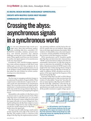
 BINARY ADDER nized to the read-clock domain before it increments the read counter. GRAY CODE TO BINARY This design requires single clockwide BINARY TO GRAY CODE pulses and pulse synchronizers for the read and write strobes because, as a level 1 signal crosses from one clock domain to a faster one, it remains valid for more POINTER (GRAY CODE) clock cycles in the faster domain than in the slow one. Because each counter The Gray-code counter, a bina- Figure 8 changes whenever the read or write ry adder, has converters from signal is valid, then the faster clock do- and to Gray code before and after the adder. main detects more reads or writes than actually occurred in the slower clock do- triggers, you must set the empty status to main. Pulse synchronizers translate a give the read circuitry time to prevent a clockwide pulse in one clock domain to read of an empty FIFO. a clockwide pulse in the new clock do- This pointer logic restricts circuits main, and each pulse represents one read from accessing the FIFO on every clock or write of the FIFO. cycle, even in the slow clock domain. The This FIFO-status technique gives pes- advantage of this feature is that the cir- simistic status for both reads and writes. cuits accessing the FIFO have at least one The status for the write port indicates full clock cycle to evaluate the FIFO status. when the FIFO has all entries filled and The FIFO can have every entry filled with continues to indicate full after the read data without overwriting valid data or strobe triggers, because synchronization can be empty without reading invalid delays the strobe to the write counter. data. Another advantage of this design is This situation is also true for the empty that each side can read its respective status on the read port, because syn- counter and determine how many entries chronization delays the write strobe to are available. A designer can use this FIFO the read counter. design for circuits that perform multiple Another consideration for this design reads or writes of data without causing an is detecting full or empty at the right underflow or overflow condition. time. If the FIFO has one entry remain- The drawback of this design is that ing, and the write strobe triggers, the counters, rather than direct comparisons FIFO must then set the full status. This of the read and write pointers, determine scenario gives the full indication one status. For large FIFOs, these counters are clock sooner to allow the circuit writing large. Also, the average data rates are half into the FIFO enough time to stop the the slowest clock frequency, because the next write from overflowing the FIFO. read or write pulses from the faster clock This situation is also true for the read domain must have at least two clock pe- port of the FIFO. In this case, if the FIFO riods between them in the slow-clock do- has only one entry, and the read strobe main when using pulse synchronizers. One way to eliminate some of these TABLE 3—GRAY CODE VERSUS problems is to use direct pointer com- parison. BINARY CODE In this FIFO design, comparing the Decimal Binary Gray read and write pointers determines the 0 0 0 FIFO status. Pointer comparison in asyn- 1 1 1 2 10 11 chronous designs is more challenging, 3 11 10 because each pointer exists in a different 4 100 110 clock domain, and synchronizing a sig- 5 101 111 nal bus requires that the bus does not 6 110 101 change while synchronizing handshake 7 111 100 signals. A FIFO design using this tech- 8 1000 1100 nique for pointer synchronization would 9 1001 1101 10 1010 1111 be slow. To solve this problem, the FIFO 11 1011 1110 pointer logic uses Gray code instead of 12 1100 1010 binary code for the pointers. 13 1101 1011 Gray code changes only one bit at a 14 1110 1001 time for each increase or decrease in the 15 1111 1000 count (Table 3). You can use synchroniz- 68 edn | July 29, 2003 www.edn.com
  • 7. ers on Gray-code buses because only one nals that cross clock domains from caus- signal changes each time the bus changes, ing unpredictable behavior in circuits, use eliminating the race condition between synchronization. Level synchronizers bits of the Gray-coded bus as it passes work well for signals that remain valid for through separate synchronizers. The many clock cycles. Use an edge-detecting pointers for this design are Gray-code synchronizer for level signals in the slow- counters. Using binary pointers would re- er clock domain that change to pulses in quire synchronizing pointer values after the new clock domain. Finally, use pulse converting them to Gray code, and using synchronizers for pulses crossing clock conversion logic violates the restriction domains. Remember that, when a signal that synchronized signals originate from bus crosses clock domains, it needs to ar- flip-flops before crossing a clock domain. rive in the new clock domain during the The Gray-code counter is a binary same clock cycle. Do not synchronize each adder with converters from and to Gray signal but use a holding register and code before and after the adder (Figure handshaking. Handshaking indicates 8). Converting to and from Gray code is when signals in the holding register are an XOR operation, so you need only a few valid and when to sample them. Using more levels of logic than a binary count- handshaking and a holding register is use- er. To convert Gray code to binary, use: ful for data buses but does not provide for B N G N; BN 1 BN GN 1;BN 2 passing more than one data word at a time BN 1 GN 2...B1 B2 G1; B0 B1 G0. to the new clock domain. To convert binary to Gray code, use: G N B N; GN 1 BN BN 1;GN 2 References BN 1 BN 2...G1 B2 B1; G0 B1 B0. 1. Davis, Leroy, Logic Metastability, A design can use the same technique to www.interfacebus.com/Design_MetaSta compare Gray-code pointer values by ble.html, September 2002. adding converters between the pointers 2. Seed, Luke, Introduction to VLSI/ and binary-comparison logic. Clocked CMOS Circuits, The University of A FIFO with this pointer logic is fast, Sheffield, UK, www.shef.ac.uk/eee/ and circuits can read or write the FIFO teach/resources/eee310/documents/VLSI on every clock cycle. However, accessing _Clocked_CMOS.pdf, February 2002. the FIFO on every cycle means the FIFO 3. Haseloff, Eilhard, “Metastable Re- status has to include almost-full and al- sponse in 5-V Logic Circuits,” Texas In- most-empty indications, so that the cir- struments Application Note SDYA006, cuits accessing the FIFO have time to www-s.ti.com/sc/psheets/sdya006/ stop. Almost full indicates that one entry sdya006.pdf, February 1997. is available to write, and almost empty 4. Cummings, Clifford E, “Synthesis indicates that one entry remains unread. and Scripting Techniques for Designing This situation describes a design that Multi-Asynchronous Clock Designs,” needs the fewest possible status signals, Synopsys Users Group Conference, San and a design needs more indicators if the Jose, CA, www.sunburst-design.com/pa- circuits accessing the FIFO use a burst ac- pers, March 2001. cess with a fixed minimum size. 5. “A Metastability Primer,” Philips This FIFO-status technique gives pes- Semiconductors Application Note AN2- simistic status for both reads and writes. 19, www.semiconductors.philips.com/ The status on the write port indicates full acrobat/applicationnotes/AN219_1. when the FIFO fills and continues to in- pdf, Nov 15, 1989. dicate full after it the circuit reads it, be- 6. Wakerly, John F, Digital Design: Prin- cause synchronization delays the read ciples and Practices, Prentice Hall, 1990. pointer to the write-side comparison log- ic. This situation is also true for the emp- Author’s bio graphy ty status on the read side, because syn- Mike Stein is principal consulting engineer chronization delays the write pointer to at Paradigm Works (Andover, MA), where the read-side comparison logic. he works on ASIC and FPGA design, syn- Handling signals crossing clock do- thesis, and static-timing analysis. He re- mains becomes less challenging when you ceived a BSEE from Northeastern Univer- design with techniques that reduce the sity in 1995. His spare-time interests risk of communication failure between include playing video games with his son, circuits in different domains. To prevent photography, snowboarding, biking, and metastability of flip-flops receiving sig- building Lego robots. www.edn.com July 24, 2003 | edn 69