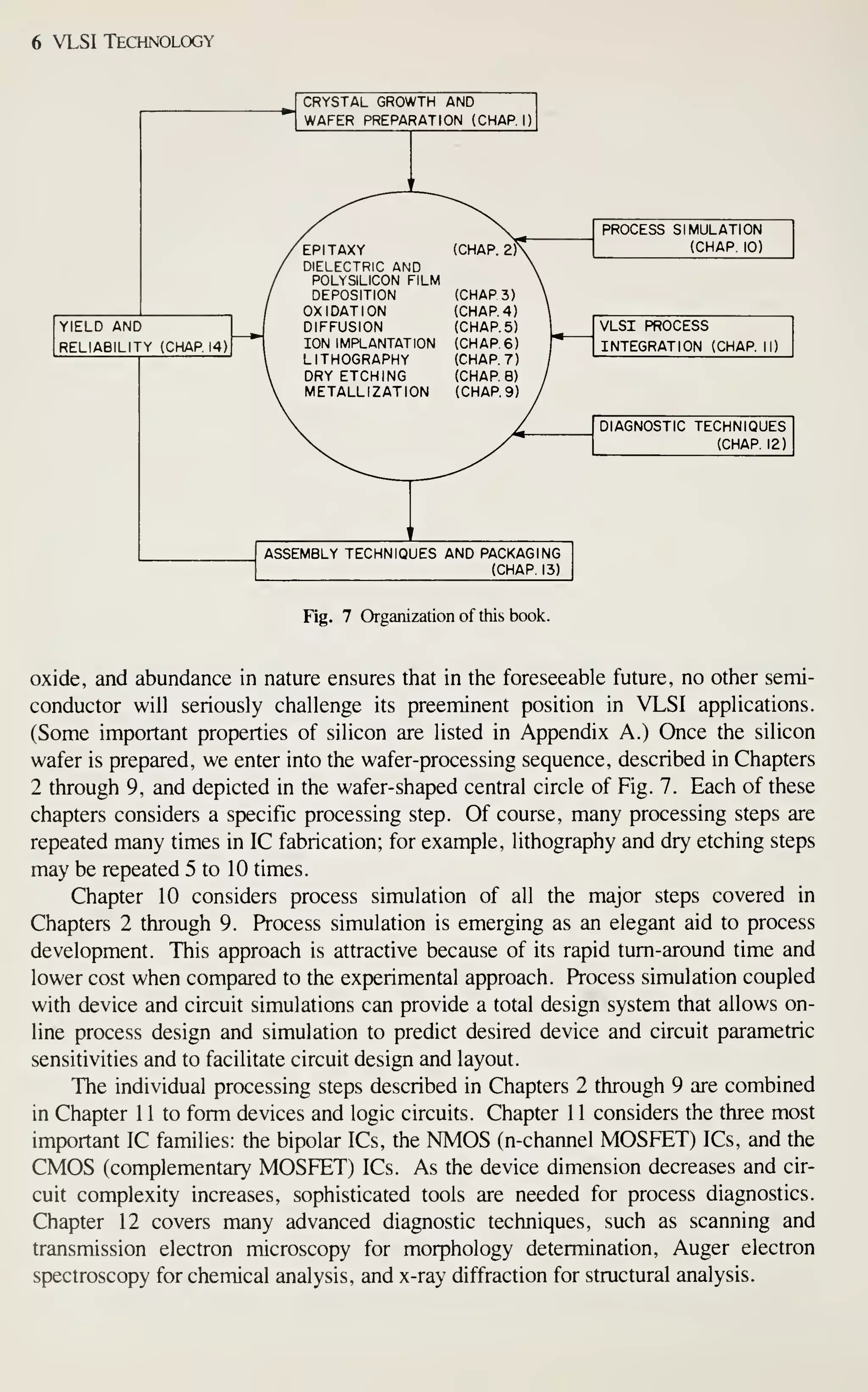
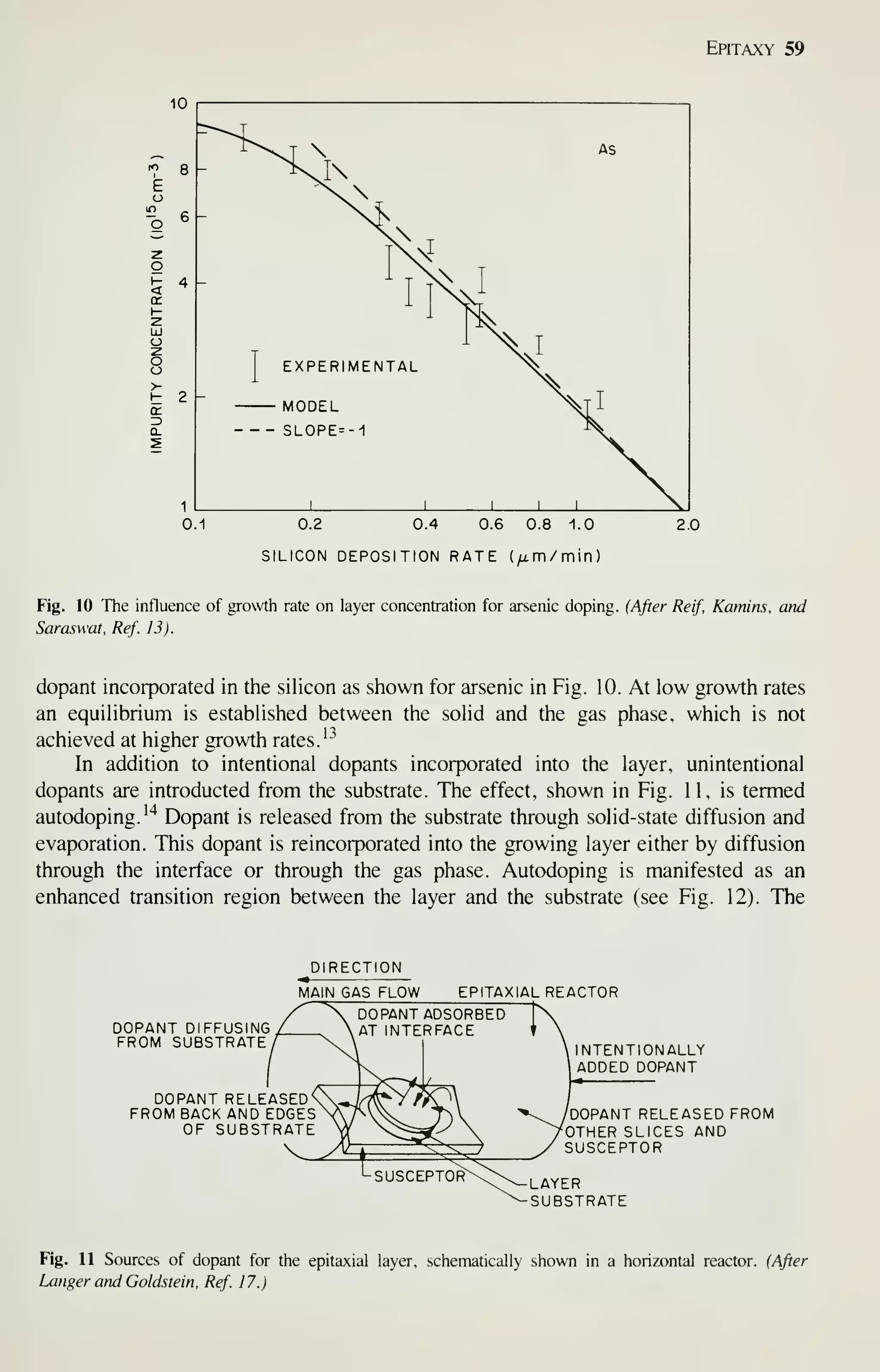
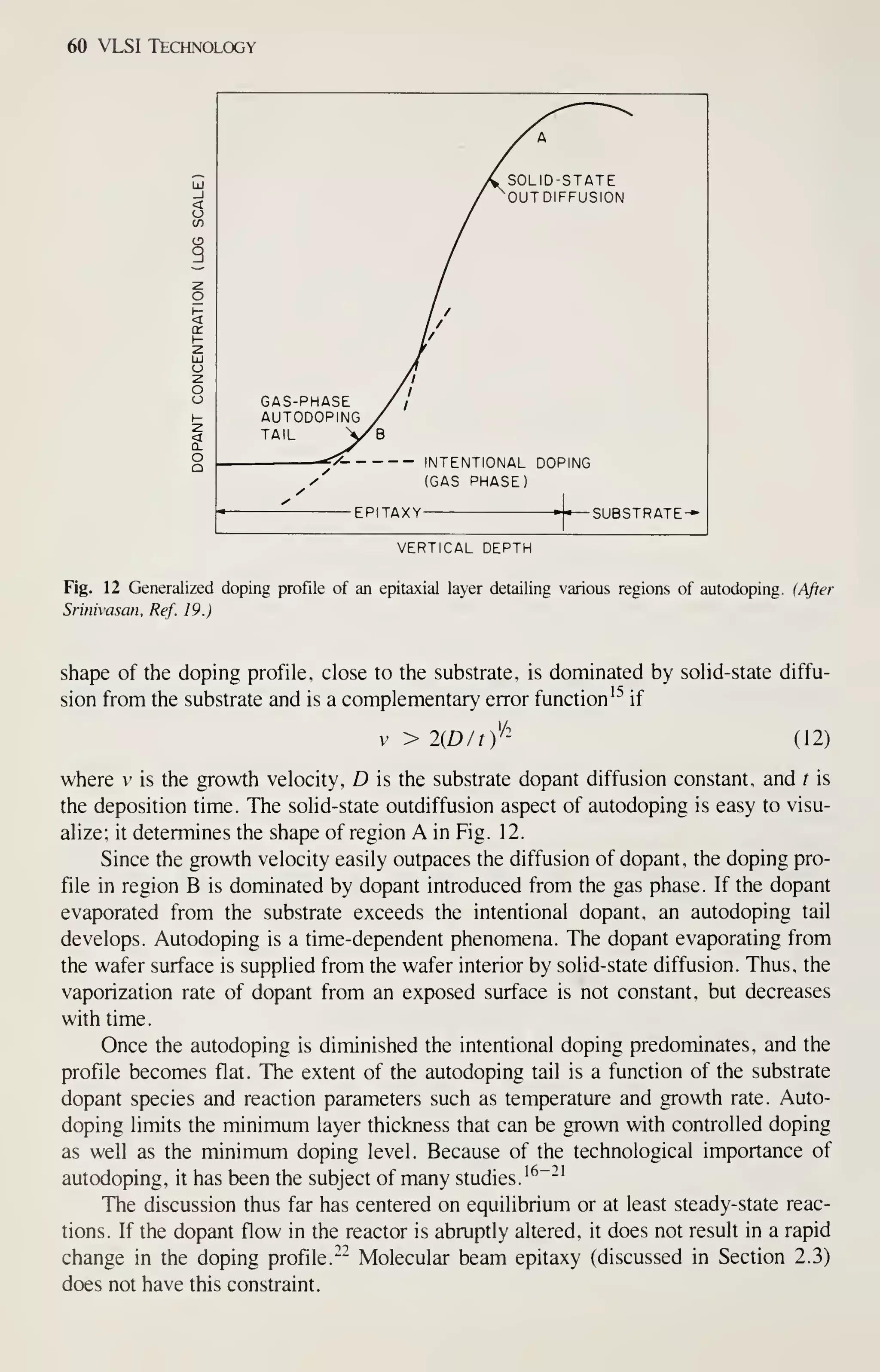
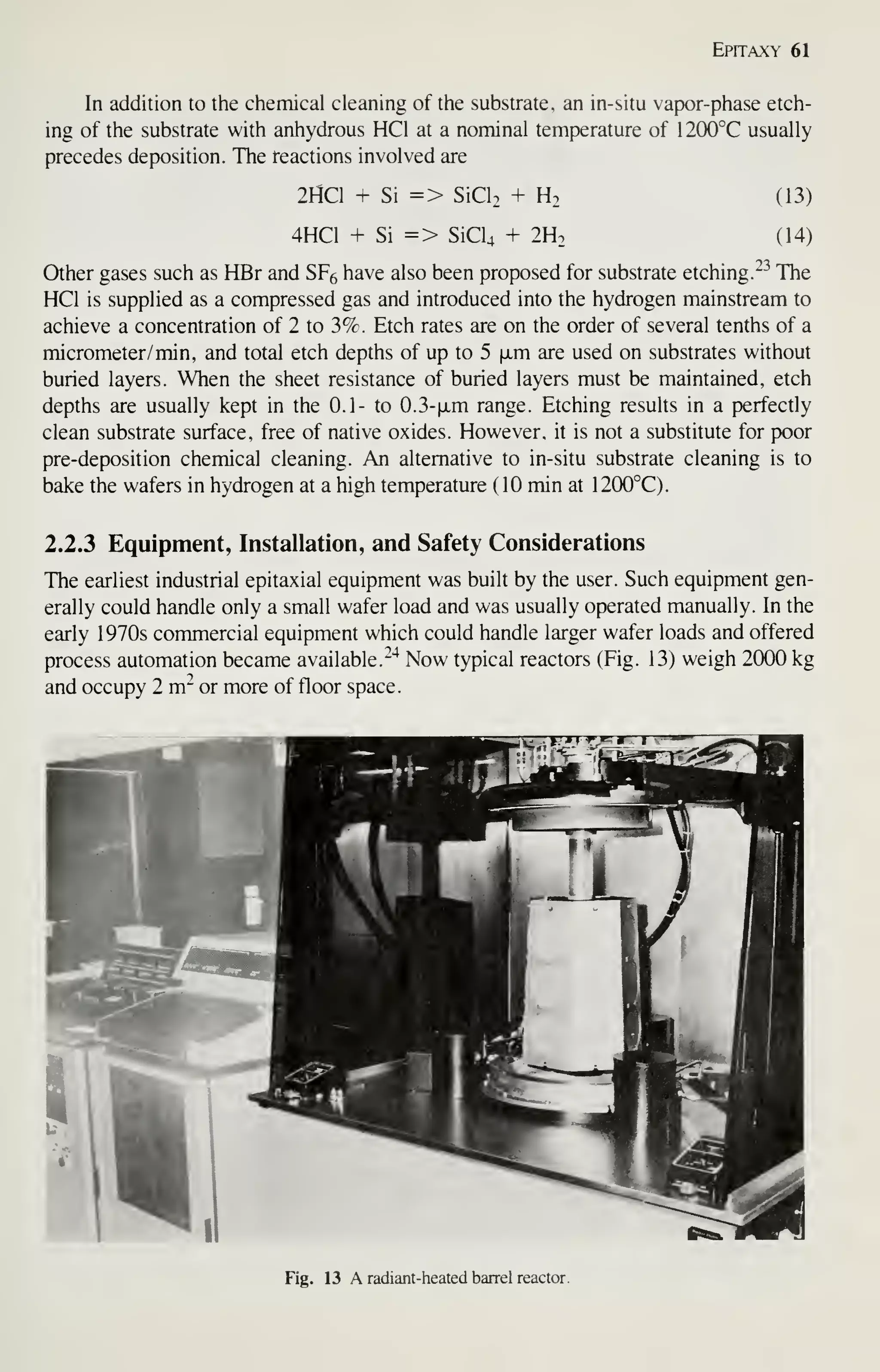
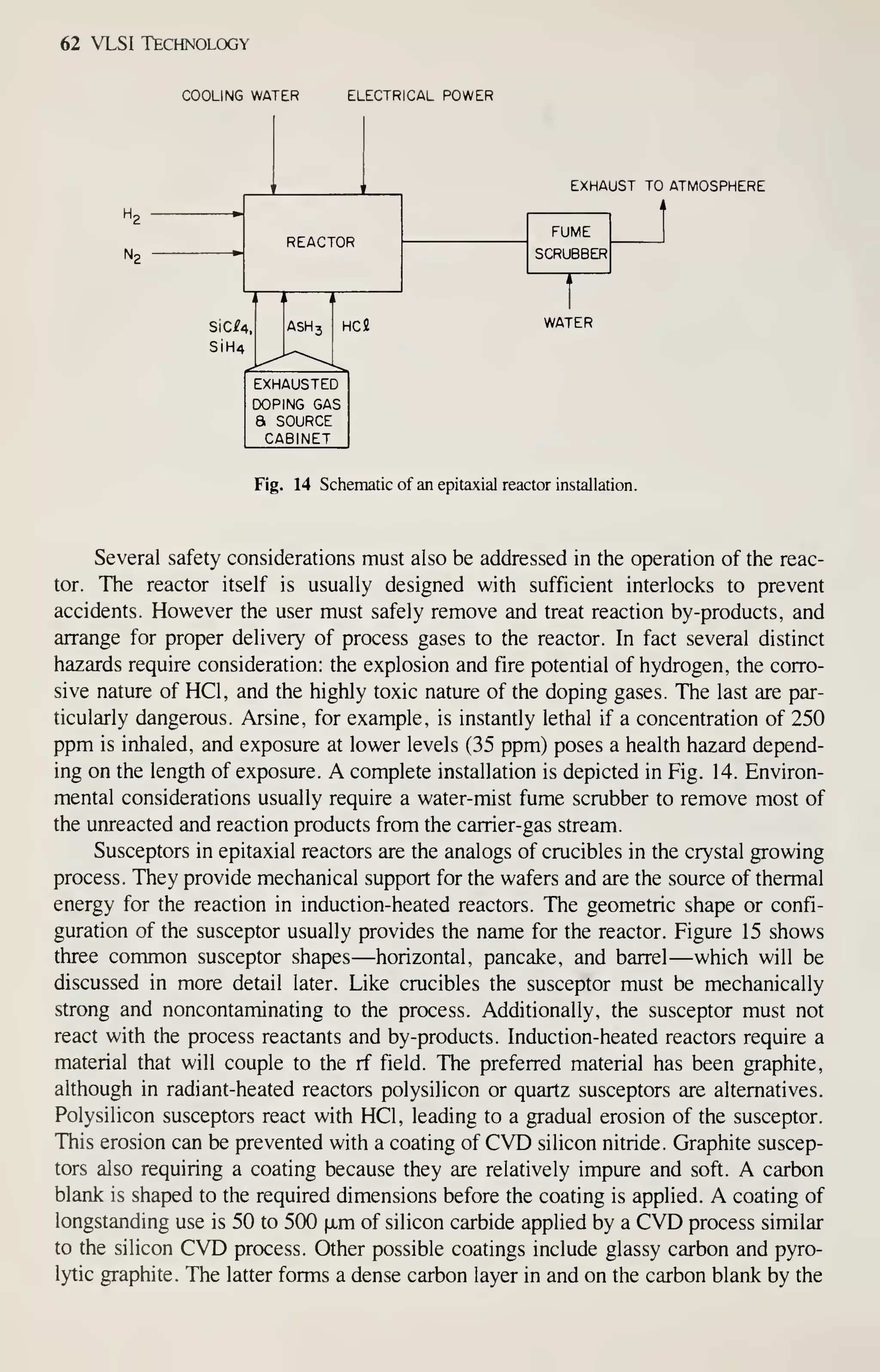
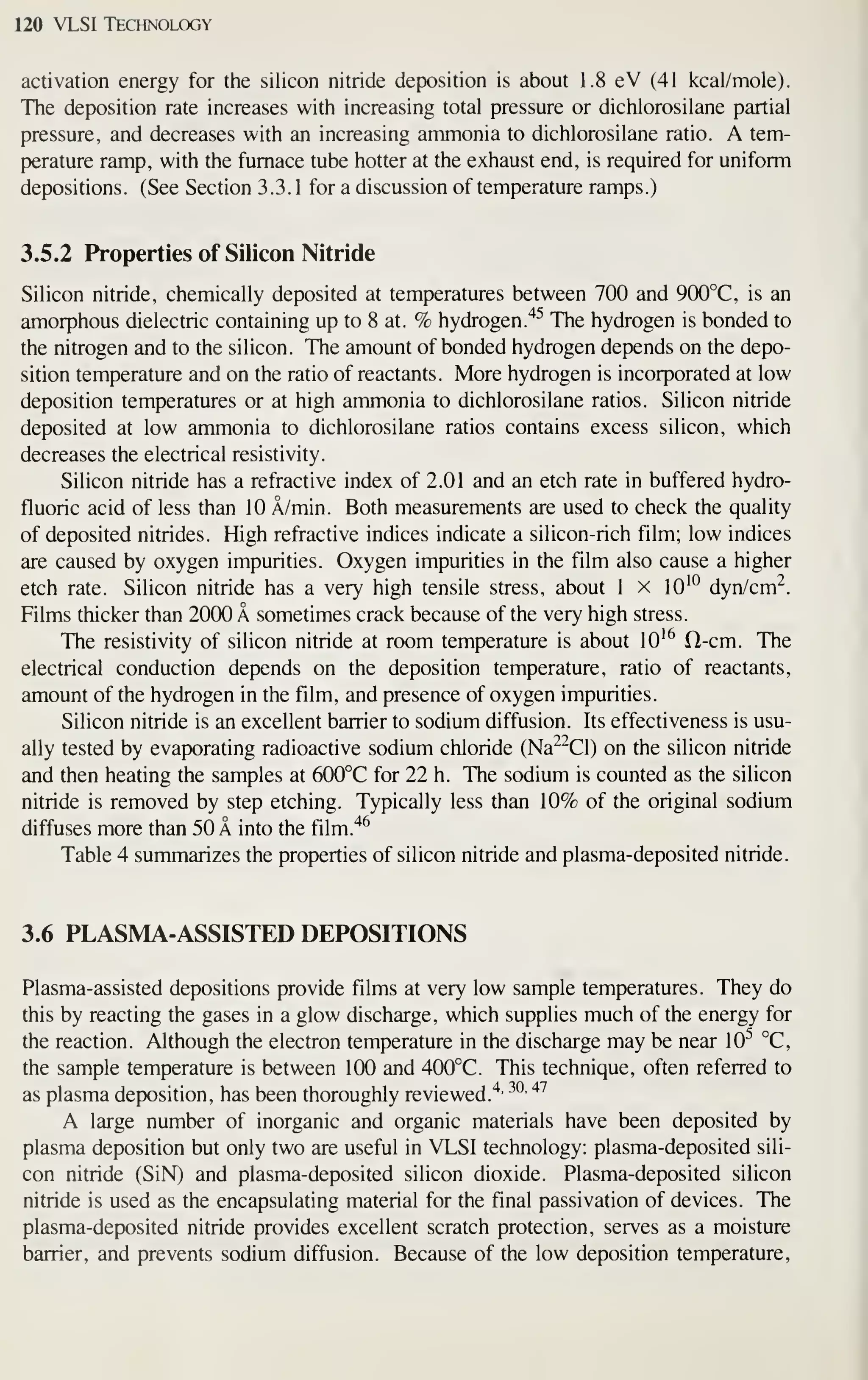
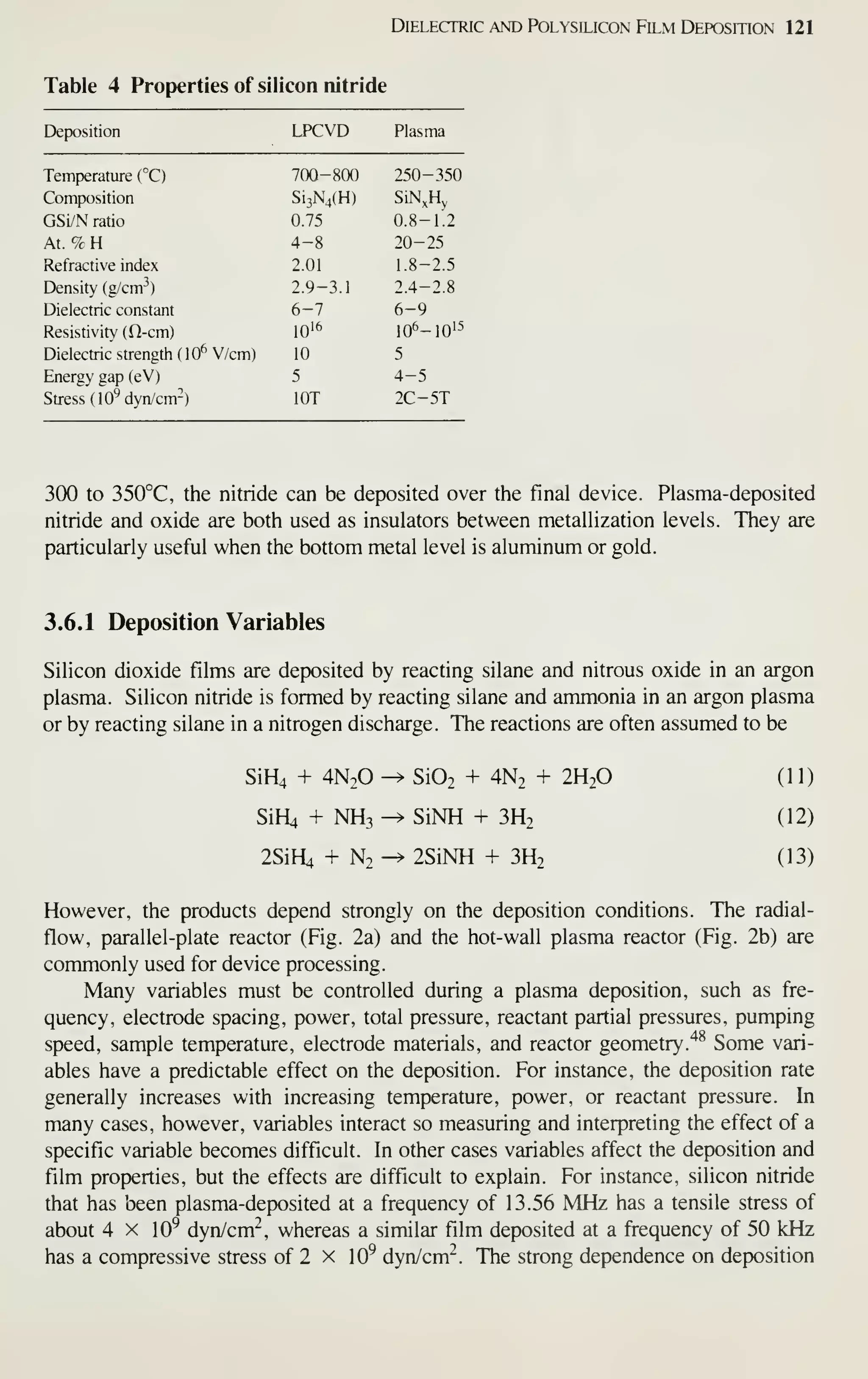
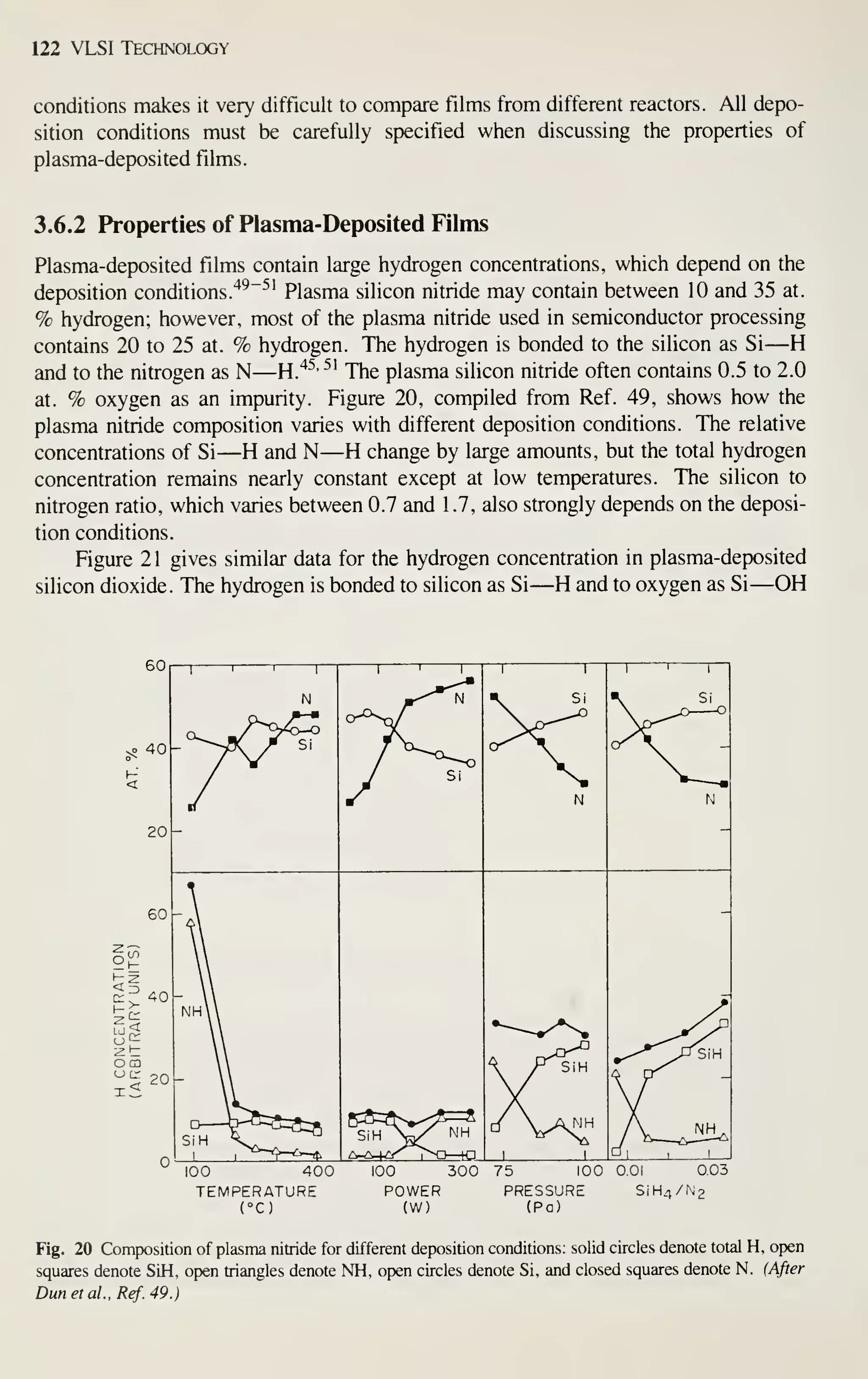
This document provides an introduction to the McGraw-Hill book "VLSI Technology" which describes the theoretical and practical aspects of very-large-scale integration (VLSI). The book covers all major steps in VLSI circuit fabrication from crystal growth to reliability testing. Each chapter focuses on one aspect of the VLSI process, providing an introduction, the underlying science, requirements for steps, and tradeoffs. The book is intended as a textbook for senior undergraduates or graduate students in electrical engineering or applied physics.


![INTRODUCTION
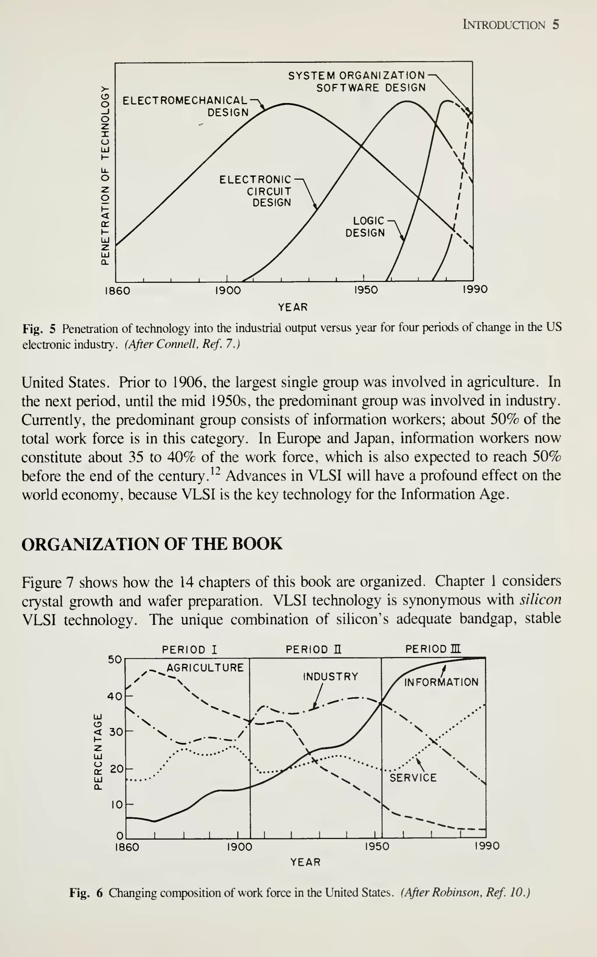
GROWTH OF THE INDUSTRY
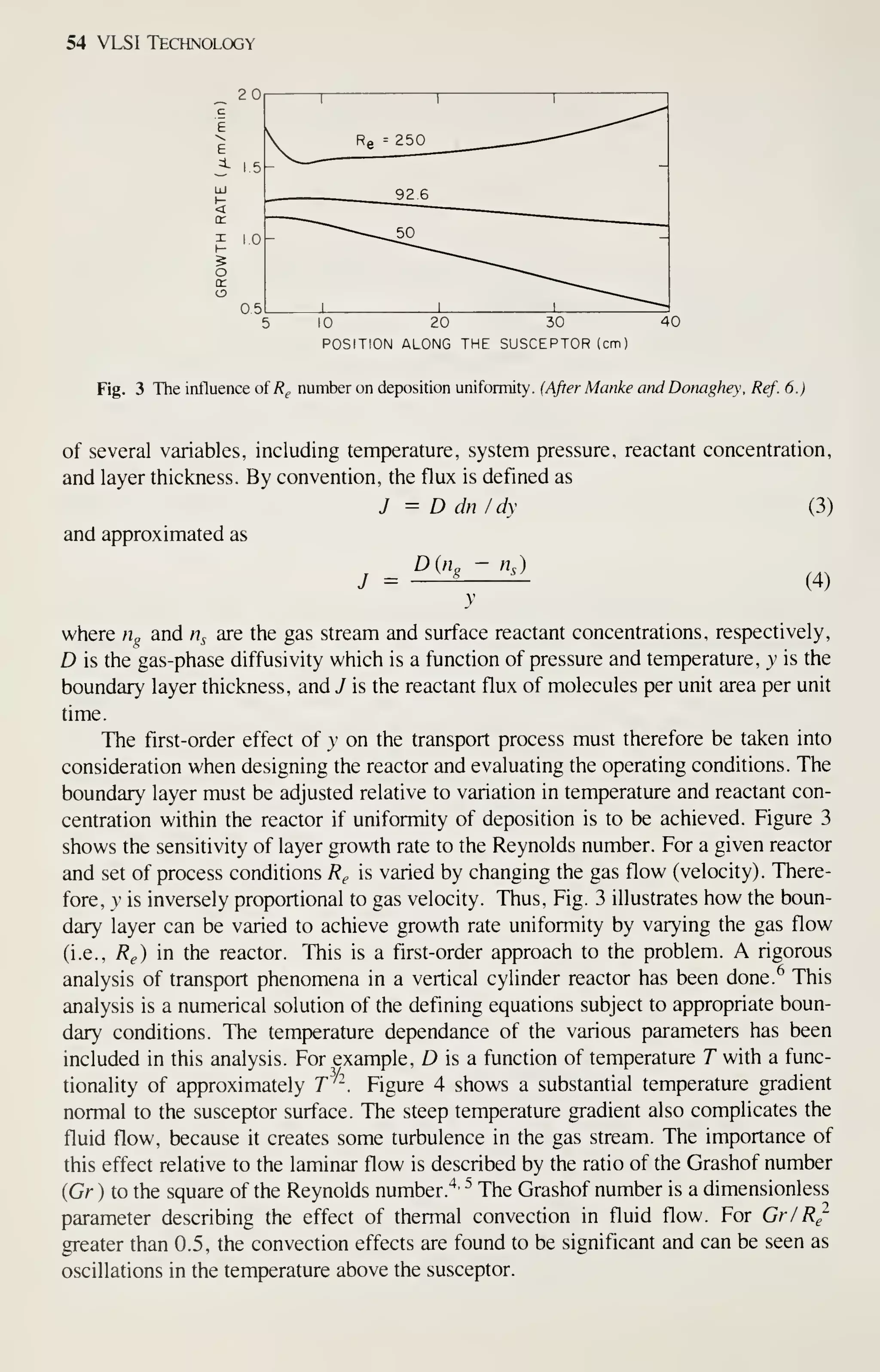
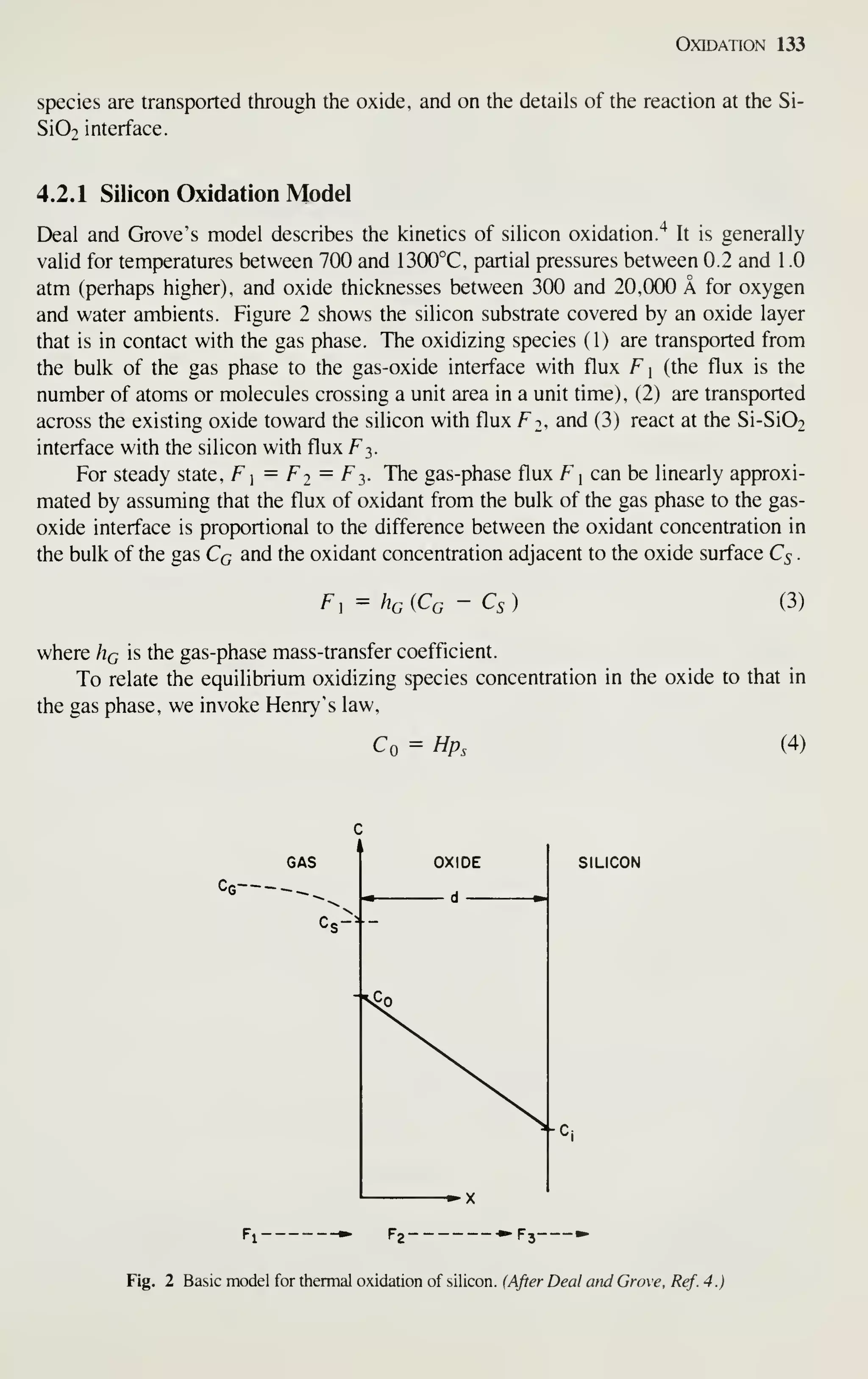
The electronics industry in the United States has grown rapidly in recent years, with
factory sales increasing by a factor of 10 since the early 1960s. [See Fig. 1, curve
(a).''^] Electronics sales, which were $114 billion in 1981, are projected to increase
at an average annual rate of 15% and finally reach $400 billion by 1990. The
integrated circuit (IC) market has increased at an even higher rate than electronic sales
[see Fig. 1, curve (b)]. IC sales in the United States were $6.6 billion in 1981 and are
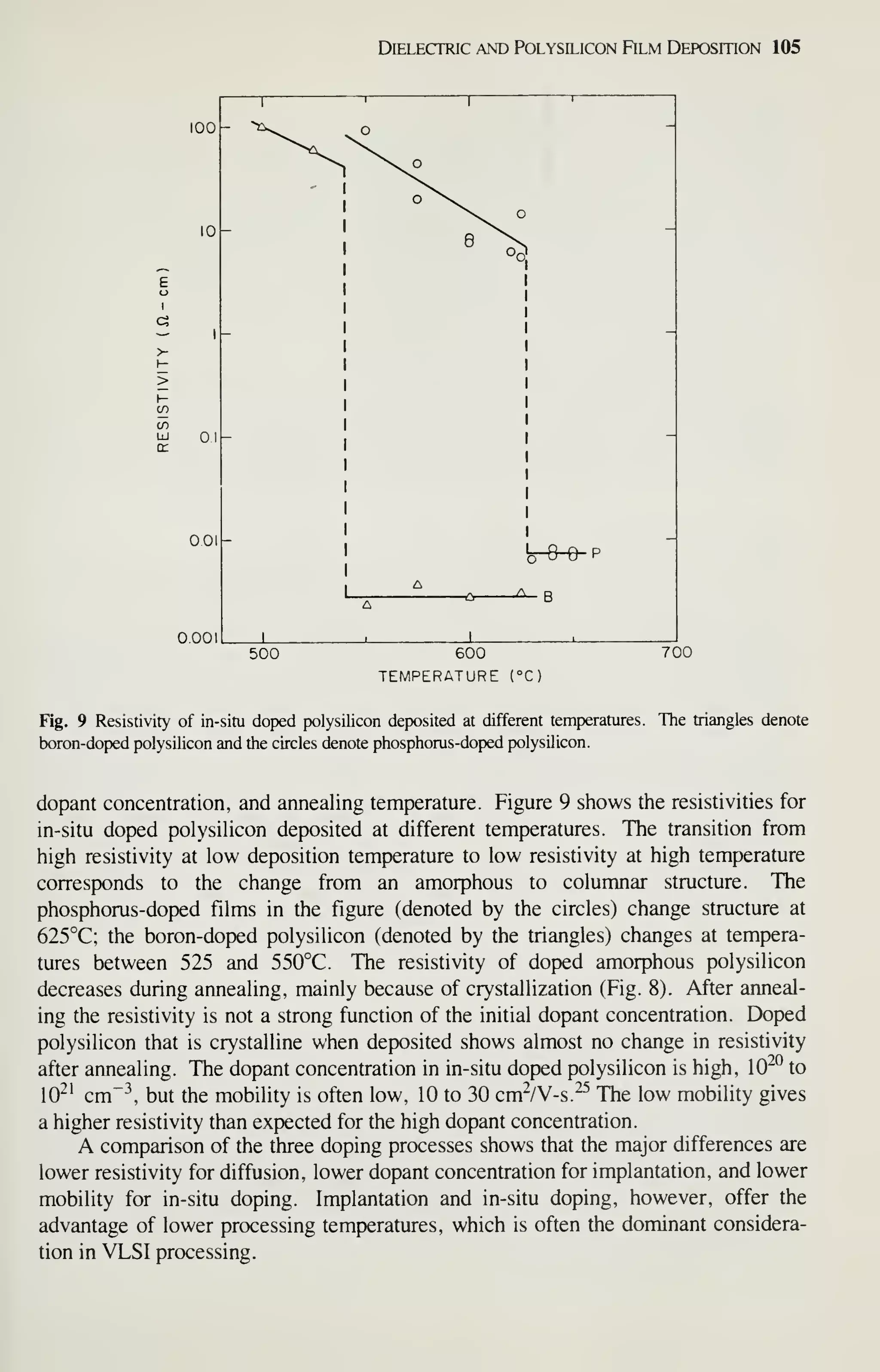
expected to grow by 25% annually, reaching $50 billion by 1990. The main
impetuses for such phenomenal market growth are the intrinsic pervasiveness of elec-
tronic products and the continued technological breakthroughs in integrated circuits.
The world market of electronics (about twice the size of the US market) will grow at a
comparable rate.^ In 10 years, it will rival the automobile, chemical, and steel indus-
tries in sales volume.
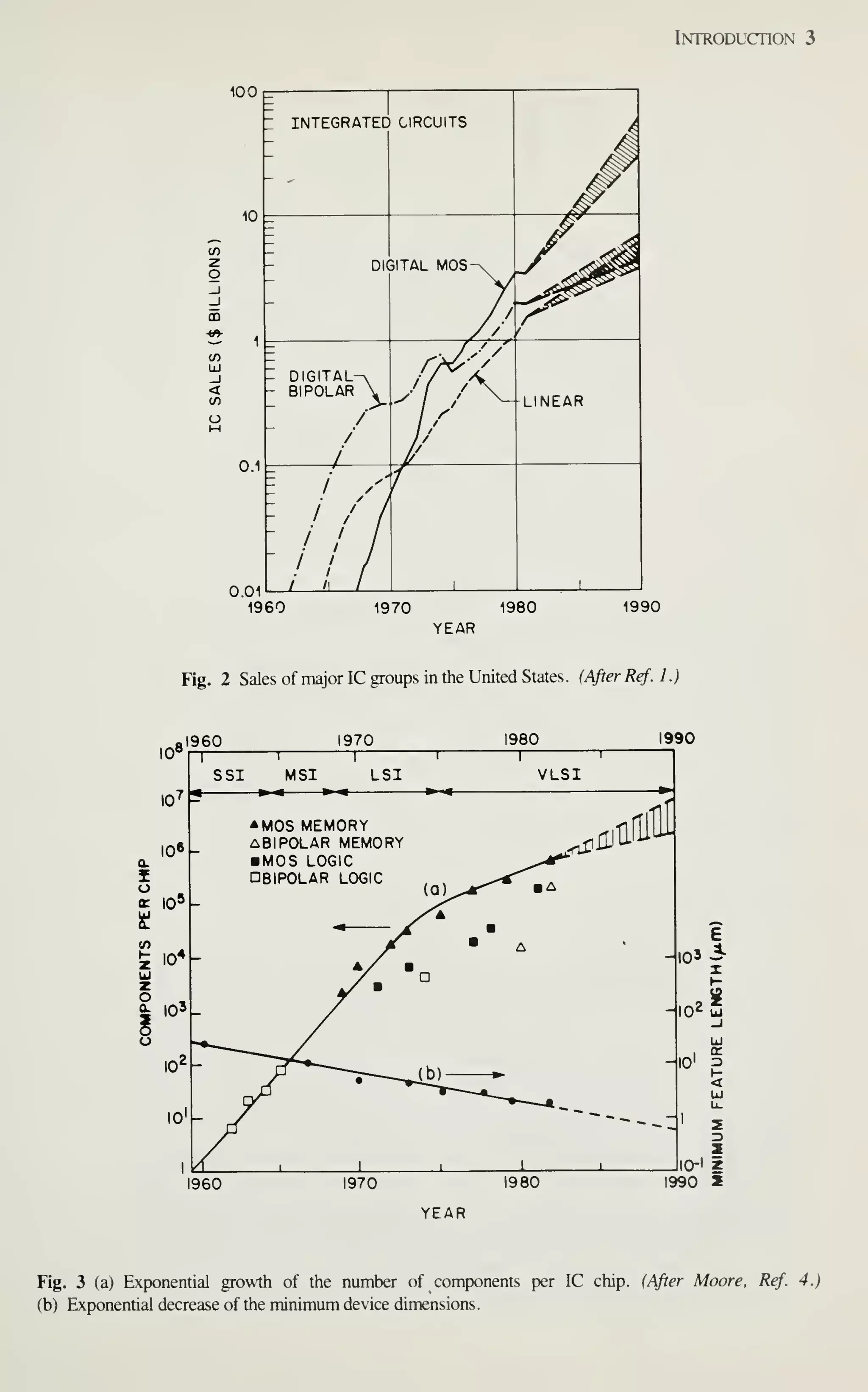
Figure 2 shows the sales of major IC groups and how sales have changed in
recent years.' In the 1960s the IC market was broadly based on bipolar transistors.
Since 1975, however, digital MOS ICs have prevailed. At present, even the intrinsic
speed advantage of bipolar transistors is being challenged by MOSFETs. Because of
the advantages in device miniaturization, low power dissipation, and high yield, by
1990 digital MOS ICs will dominate the IC market and capture a major market share
of all semiconductor devices sold. This book, therefore, emphasizes MOS-related
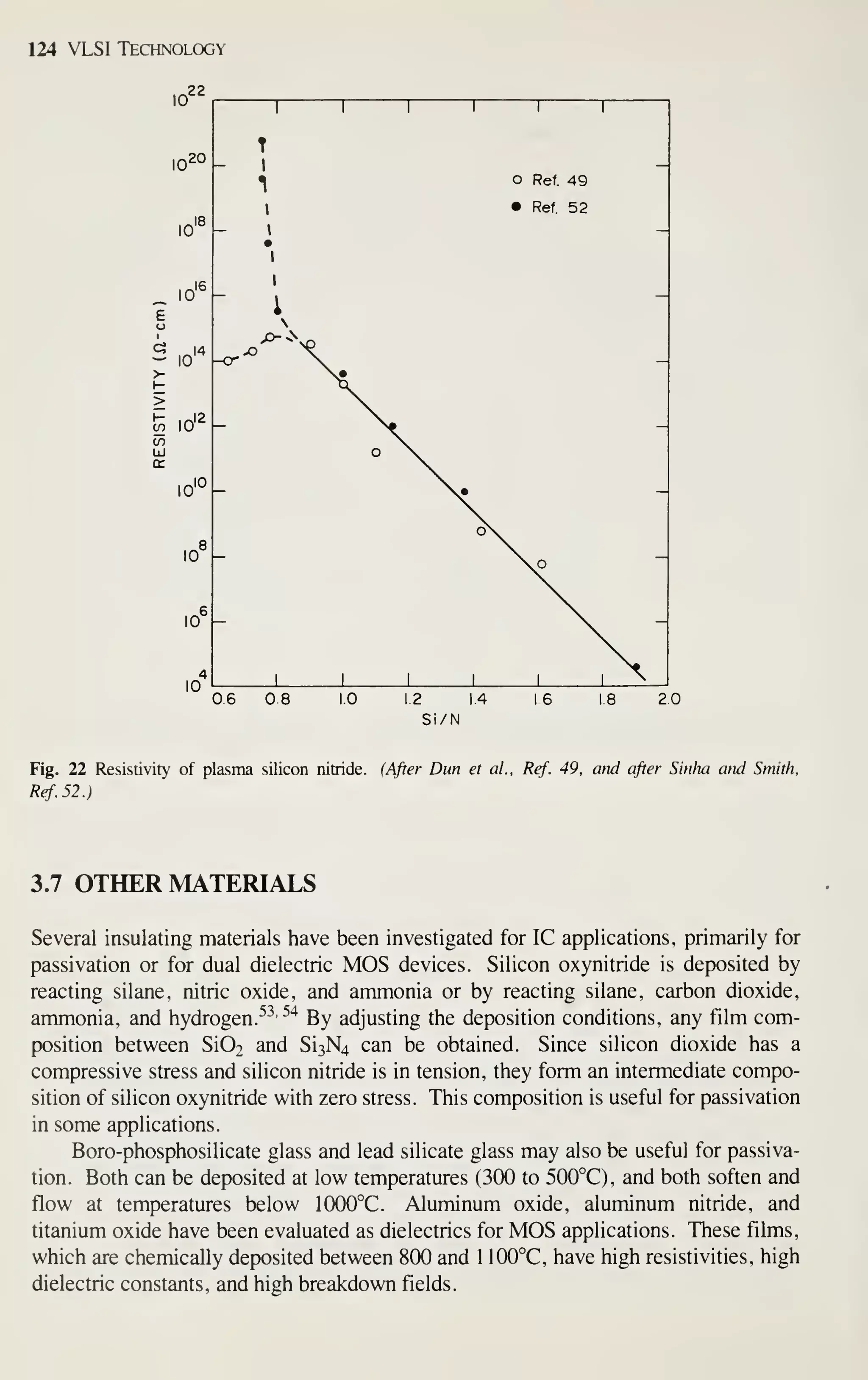
VLSI technology.
DEVICE MINIATURIZATION
Figure 3, curve (a), shows the exponential growth of the number of components per
IC chip.'^ Note that IC complexity has advanced from small-scale integration (SSI) to
medium-scale integration (MSI), to large-scale integration (LSI), and finally to very-
large-scale integration (VLSI), which has 10^ or more components per chip.](https://image.slidesharecdn.com/simonm-220913174129-44ec6f82/75/Simon-M-Sze-editor-Very-Large-Scale-Integration-VLSI-Technology-McGraw-Hill-Inc-US-1983-pdf-21-2048.jpg)
![2 VLSI Technology
1000 p
1930 1940 1950 1960 1970
YEAR
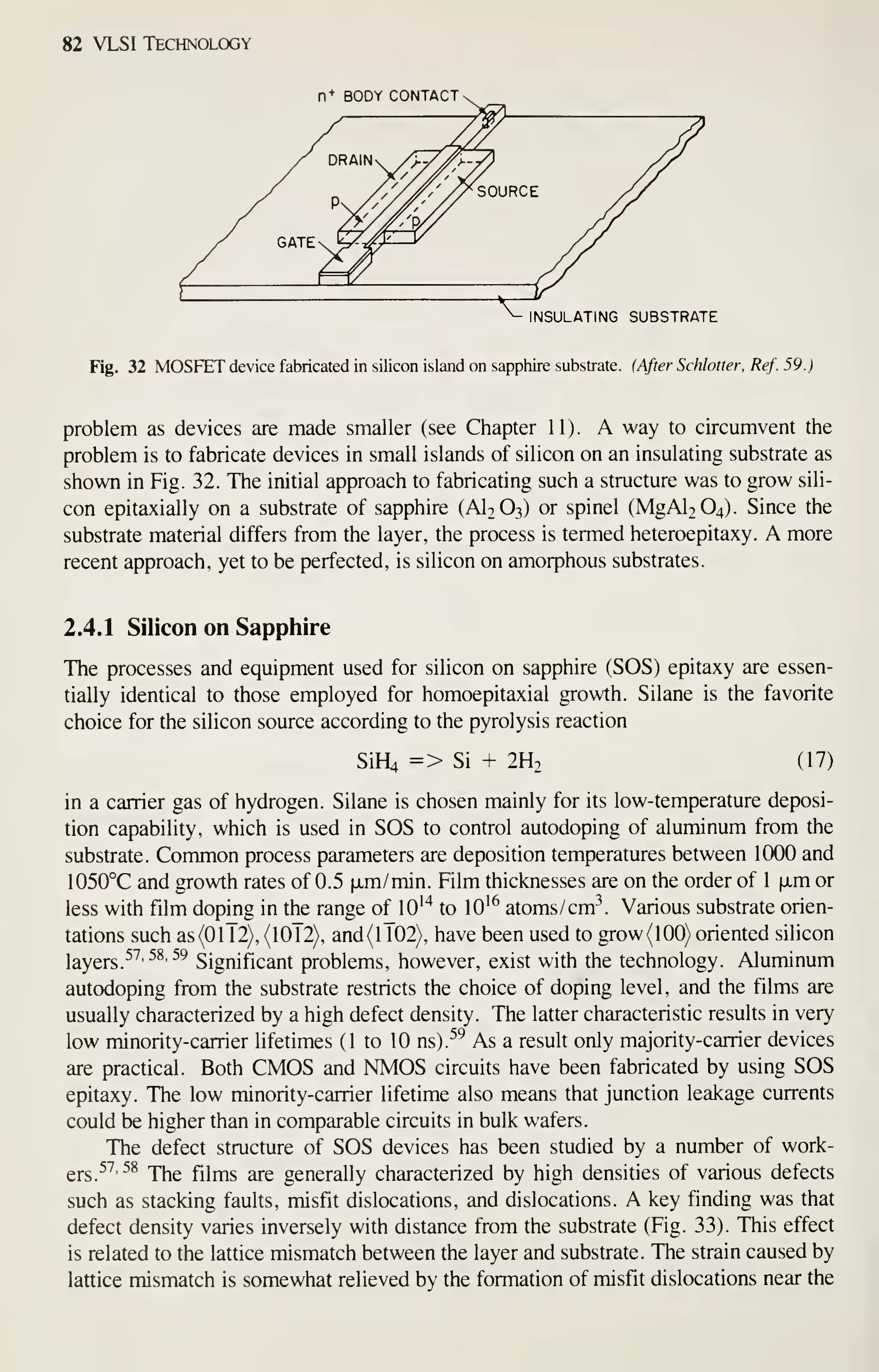
1980 1990
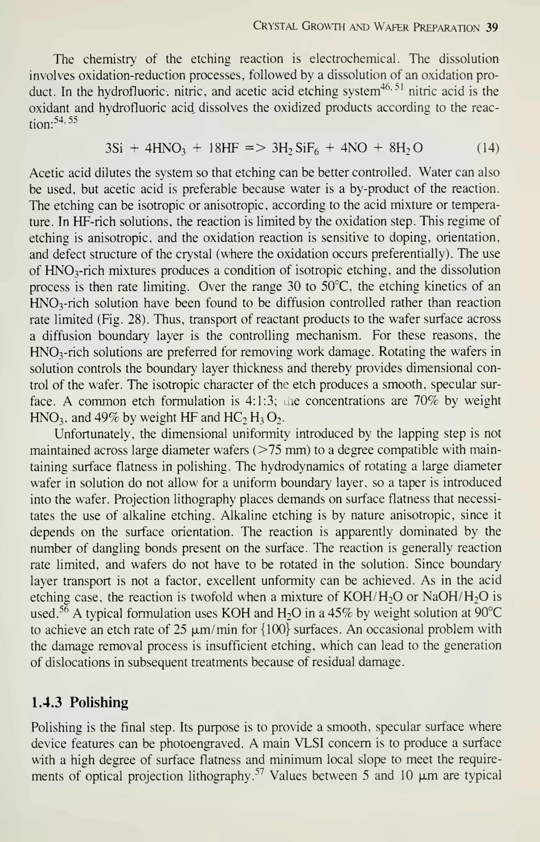
Fig. 1 (a) Factory sales of electronics in the United States for the 52 years between 1930 and 1981 and
projected to 1990. (b) Integrated circuit market in the United States for the 20 years between 1962 and
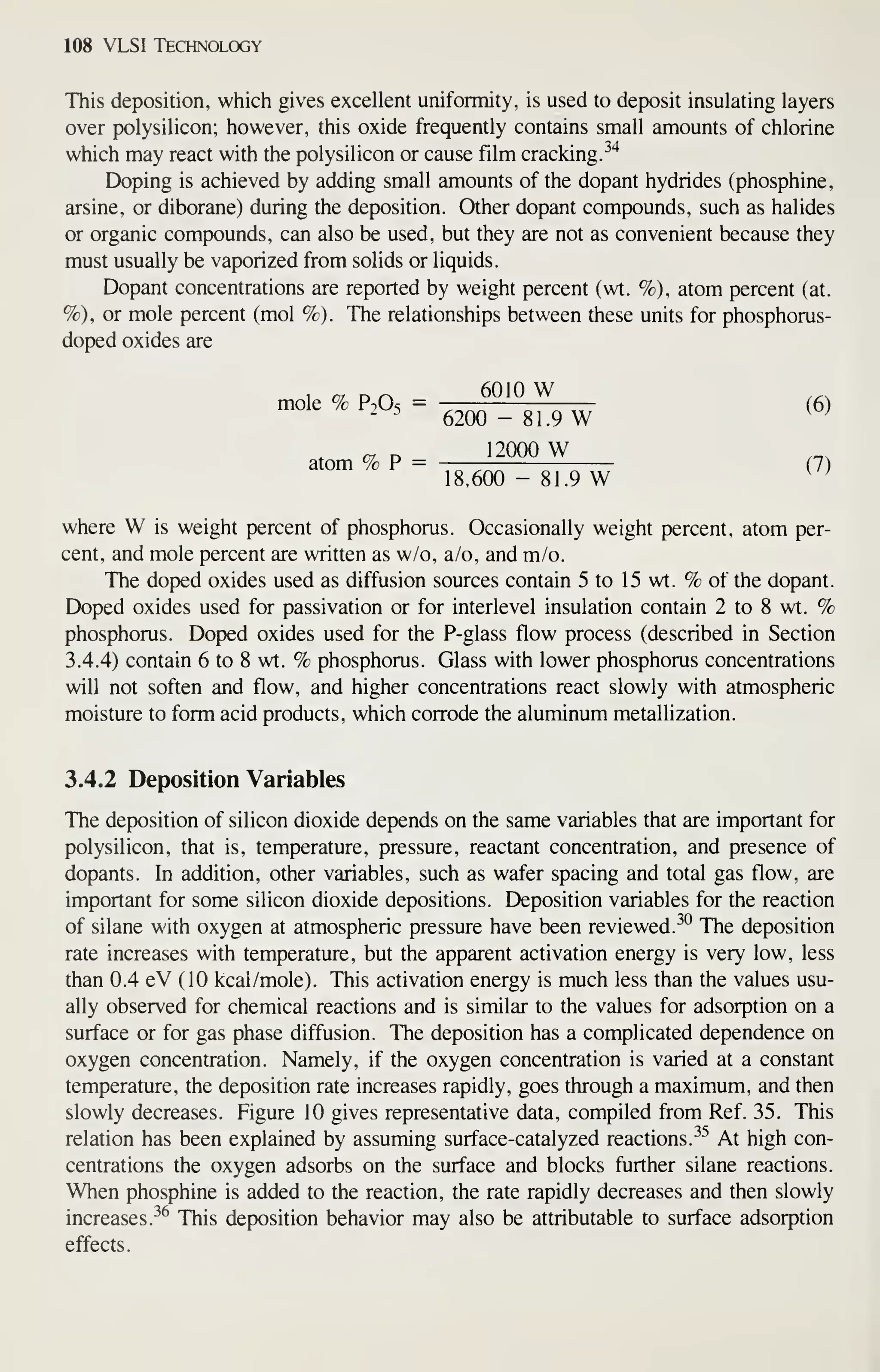
1981 and projected to 1990. (After Refs. 1 and2.)
Although the rate of growth has slowed down in recent years because of difficulties in
defining, designing, and processing complicated chips, a complexity of over 1 million
devices per chip will be available before 1990.
The most important factor in achieving such complexity is the continued reduc-
tion of the minimum device dimension [see Fig. 3, curve (b)]. Since 1960, the annual
rate of reduction has been 13%; at that rate, the minimum feature length will shrink
from its present length of 2 |xm to 0.5 fxm in 10 years.
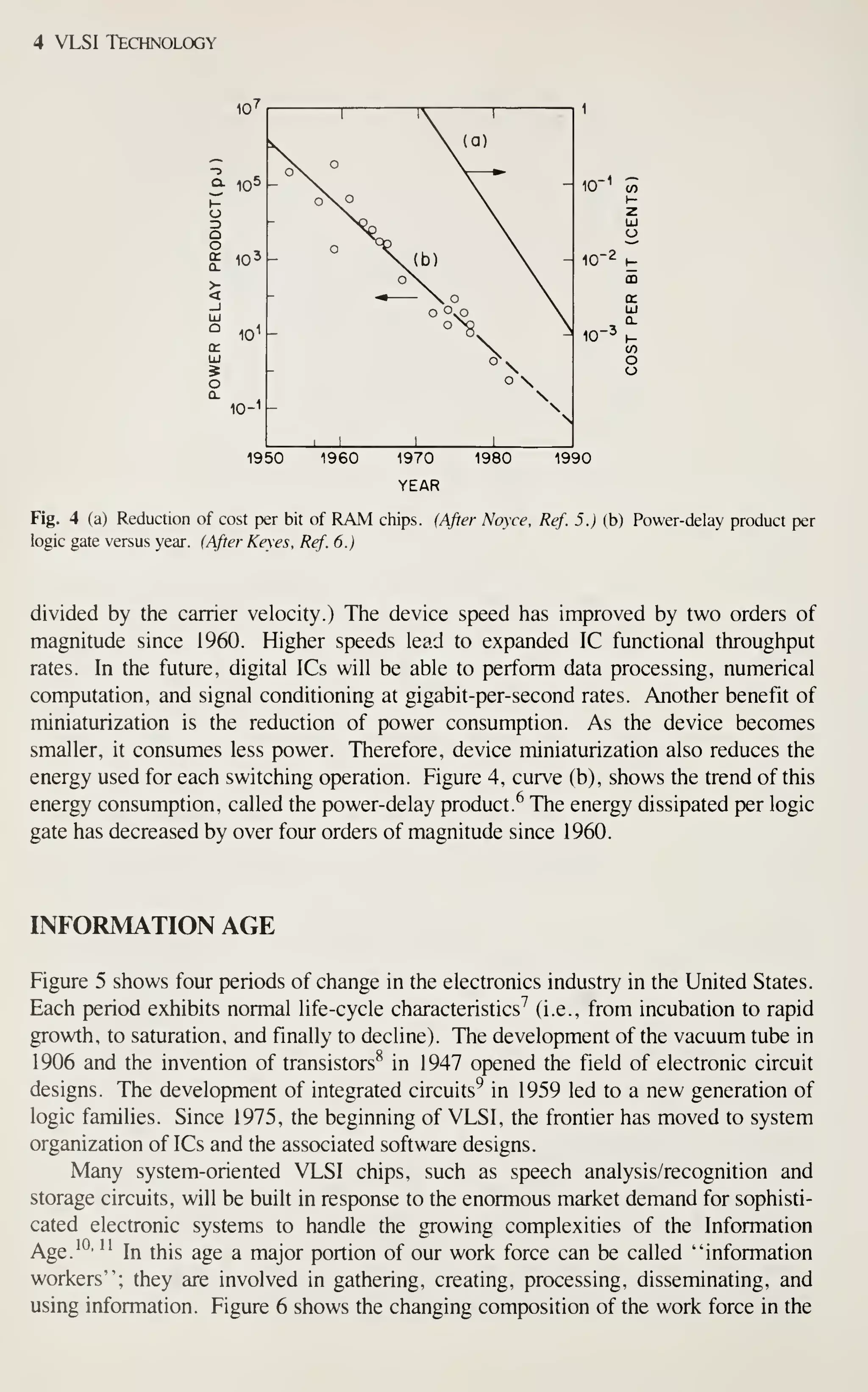
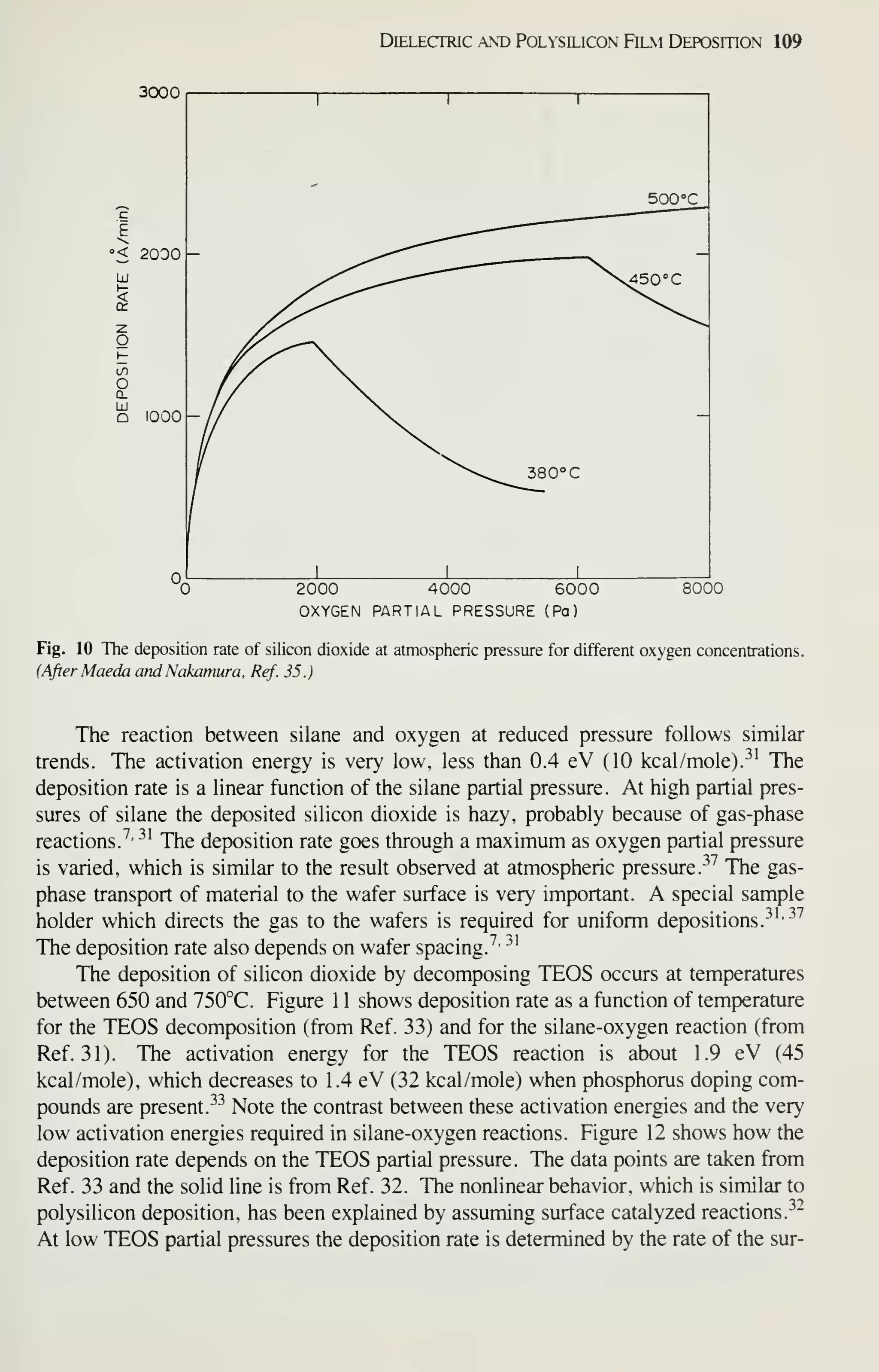
Device miniaturization results in reduced unit cost per function and in improved
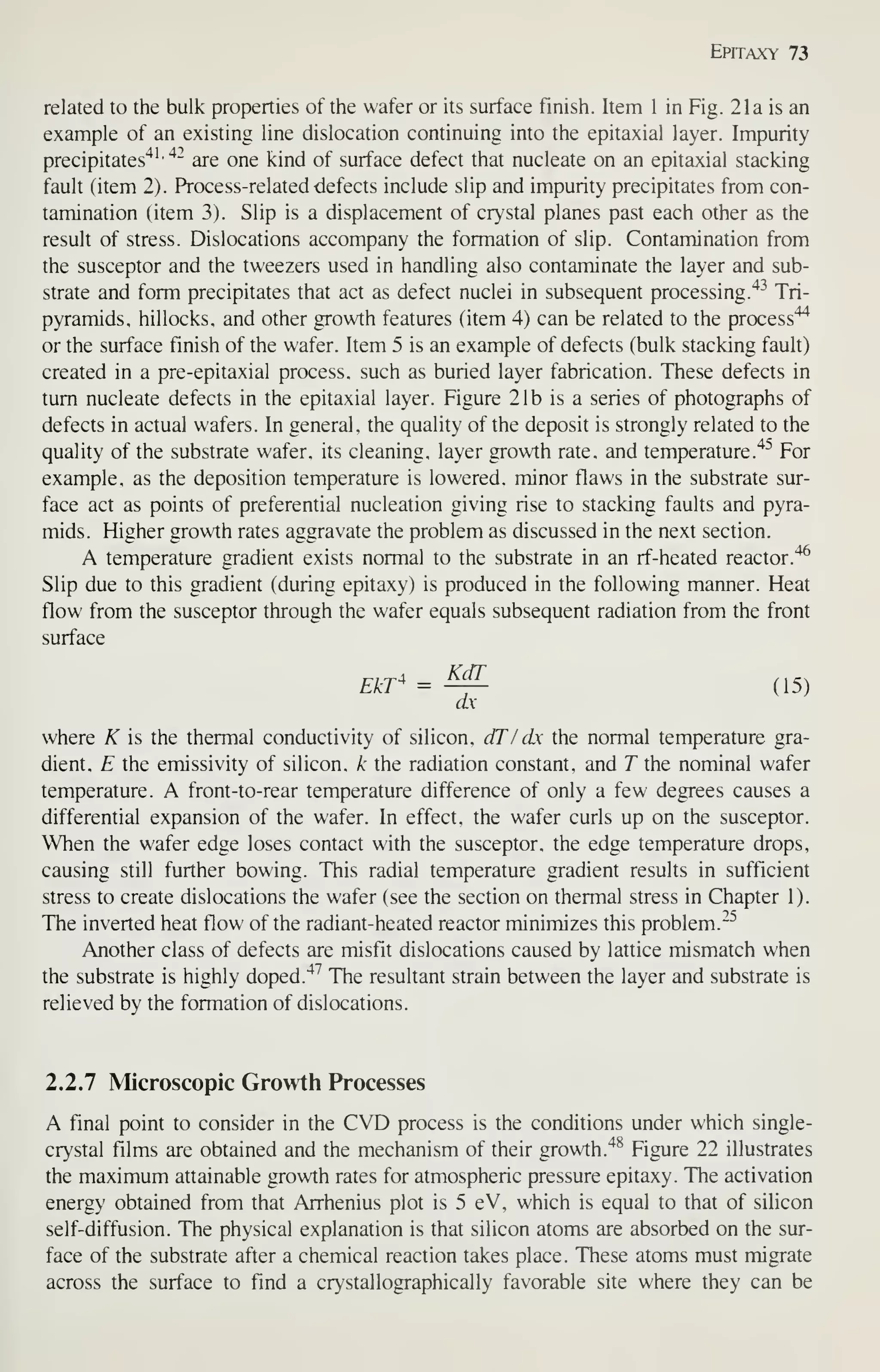
performance. Figure 4, curve (a), gives an example of the cost reduction. The cost
per bit of memory chips has halved every 2 years for successive generations of
random-access memories.^ By 1990 the cost per bit is expected to be as low as ~ 1
millicent for a 1 -megabit memory chip. Similar cost reductions are expected for logic
ICs.
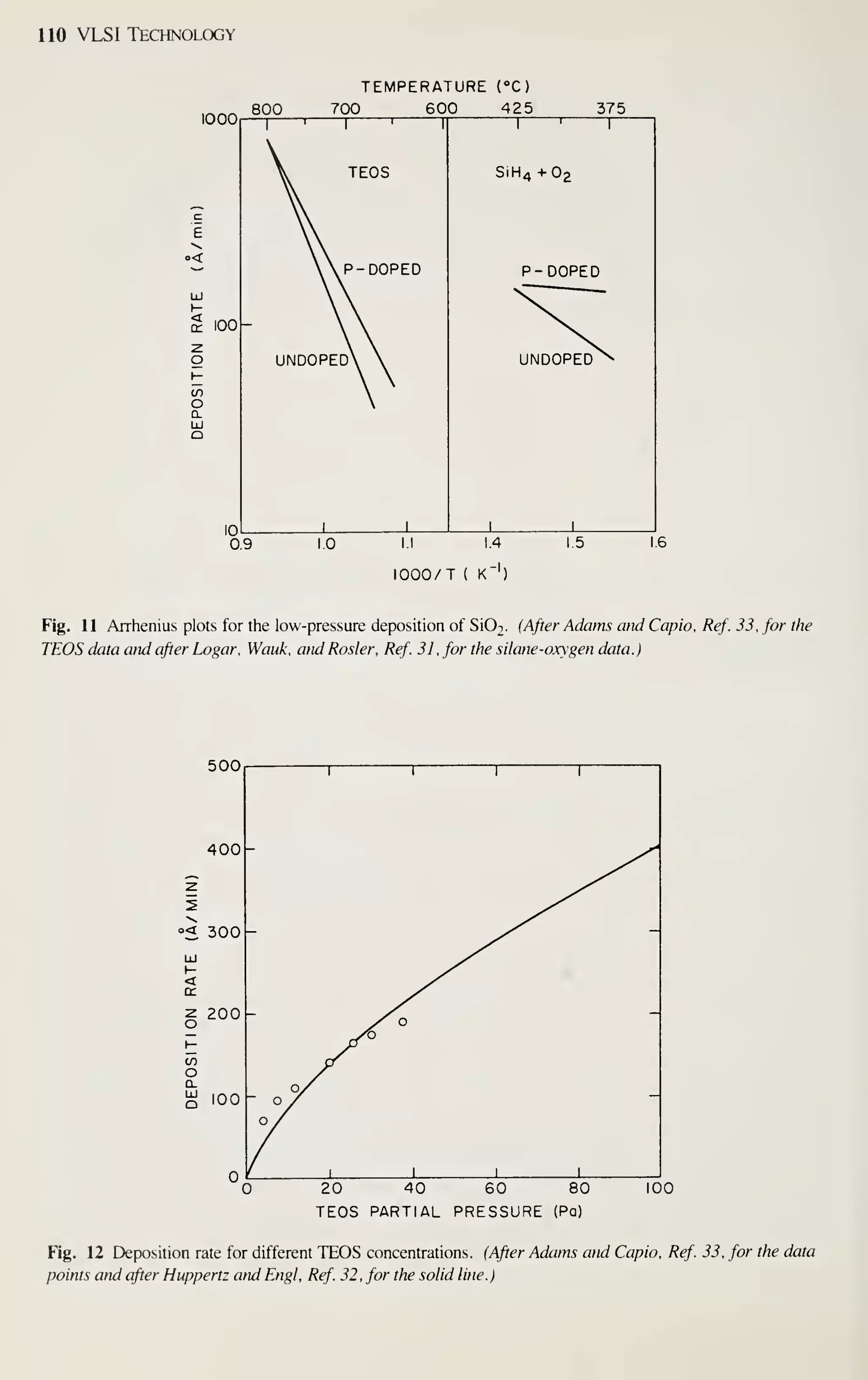
As device dimension decreases, the intrinsic switching time in MOSFETs
decreases linearly. (The intrinsic delay is given approximately by the channel length](https://image.slidesharecdn.com/simonm-220913174129-44ec6f82/75/Simon-M-Sze-editor-Very-Large-Scale-Integration-VLSI-Technology-McGraw-Hill-Inc-US-1983-pdf-22-2048.jpg)
![Introduction 7
After completely processed wafers are tested, those chips that pass the tests are
ready to be packaged. Chapter 13 describes the assembly and packaging of VLSI
chips. Chapter 14 describes the yield at every step of the processing and the reliabil-
ity of the packaged ICs. As device dimensions approach 1 ixm, VLSI processing
becomes more automated, resulting in tighter control of all processing parameters. At
every step of production, from crystal growth to device packaging, numerous refine-
ments are being made to improve the yield and reliability.
To keep the notation simple in this book, we sometimes found it necessary to use
a simple symbol more than once, with different meanings. For example, in Chapter 1
S means 4-point probe spacing, in Chapter 7 it means resist sensitivity, while in
Chapter 14 it means slope of a failure plot. Within each chapter, however, a symbol
has only one meaning and is defined the first time it appears. Many symbols do have
the same or similar meanings consistently throughout this book; they are summarized
in Appendix B.
At present, VLSI technology is moving at a rapid pace. The number of VLSI
publications (i.e., papers with the acronym "VLSI" in the title or abstract) has grown
from virtually zero in 1975 to over 1000 in 1981 with an average annual growth rate
of over 300%! Note that many topics, such as lithography and process simulation, are
still under intensive study. Their ultimate capabilities are still not fully understood.
The material presented in this book is intended to serve as a foundation. The refer-
ences listed at the end of each chapter can supply more information.
REFERENCES
[1] Electronic Market Data Book 1982, Electronic Industries Association, Washington. D.C., 1982.
[2] "World Markets Forecast for 1982," Electronics, 55, No. 1, 121 (1982).
[3] "Ten-Year Worldwide Forecast for Electronic Equipment and Components," Electronic Business,
p. 92 (February 1981).
[4] G. Moore, "VLSI. What Does the Future Hold," Electron. Aust.,4,2, 14 (1980).
[5] R. N. Noyce, "Microelectronics," in T. Forester, Ed., The Microelectronics Revolution, MIT Press,
Cambridge, Mass., 1981, p. 29.
[6] R. W. Keyes. "Limitations of Small Devices and Large Systems," in N. G. Einspruch, Ed., VLSI
Electronics, Academic, New York, 1981, Vol. 1, p. 186.
[7] J. M. Connell, "Forecasting a New Generation of Electronic Components," Digest IEEE Spring
Compcon.. SI, 14(1981).
[8] W. Shockley, "The Path to the Conception of the Junction Transistor," IEEE Trans. Electron De-
vices, ED-23, 591 {916).
[9] J. S. Kilby, "Invention of the Integrated Circuits. ""
IEEE Trans. Electron Devices, ED-23, 648
(1976).
[10] A. L. Robinson, "Electronics and Employment: Displacement Effects," in T. Forester, Ed., The
Microelectrons Revolution, MIT Press, Cambridge, Mass., 1981, p. 318.
[11] J. S. Mayo, "Technology Requirements of the Information Age," Bell Lab. Rec, 60, 55 (1982).
[12] D. Kimbel, Microelectronics, Productivity and Employment, Organization for Economic Coopera-
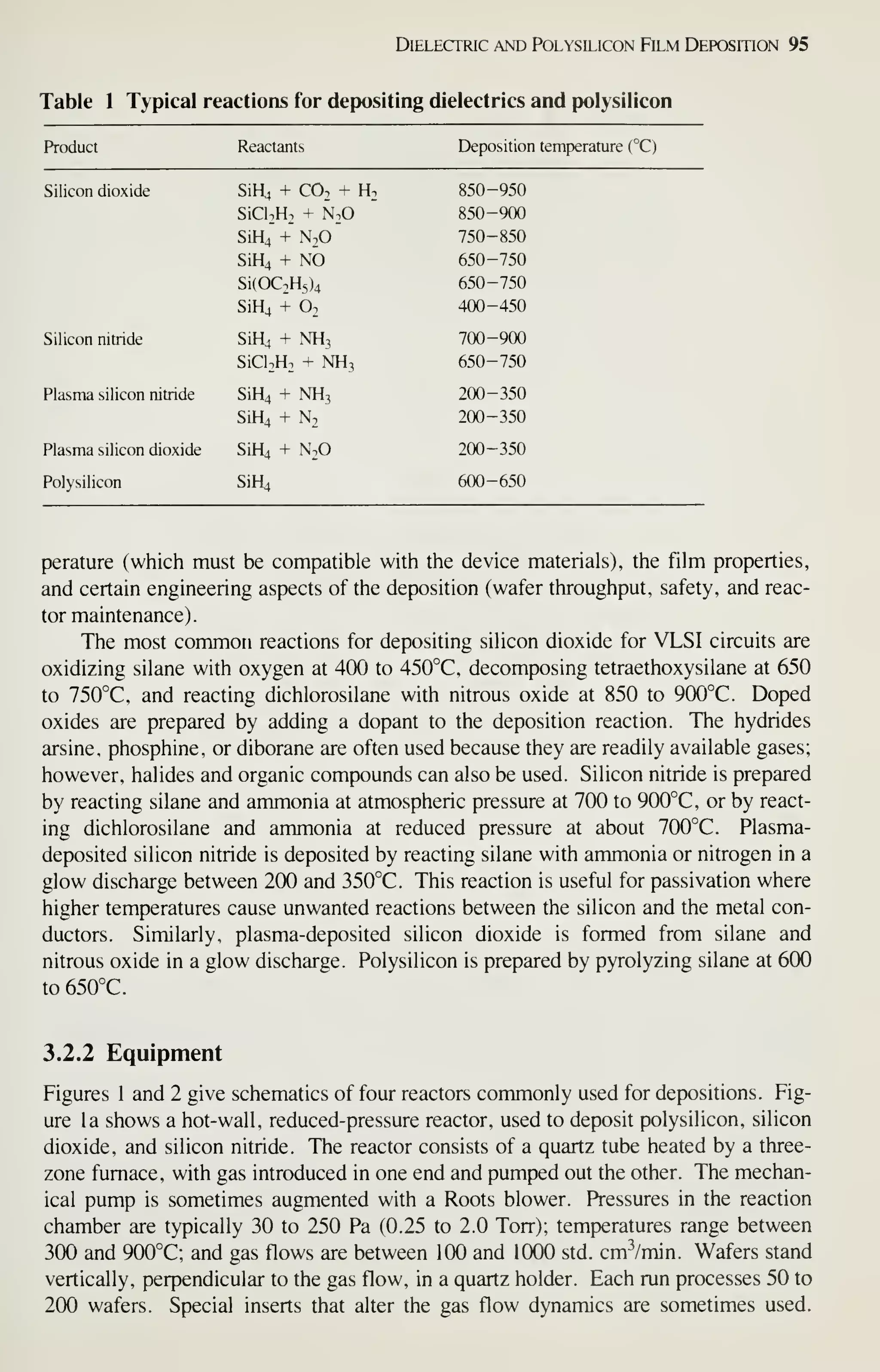
tional Development, Paris, 1981, p. 15.](https://image.slidesharecdn.com/simonm-220913174129-44ec6f82/75/Simon-M-Sze-editor-Very-Large-Scale-Integration-VLSI-Technology-McGraw-Hill-Inc-US-1983-pdf-27-2048.jpg)

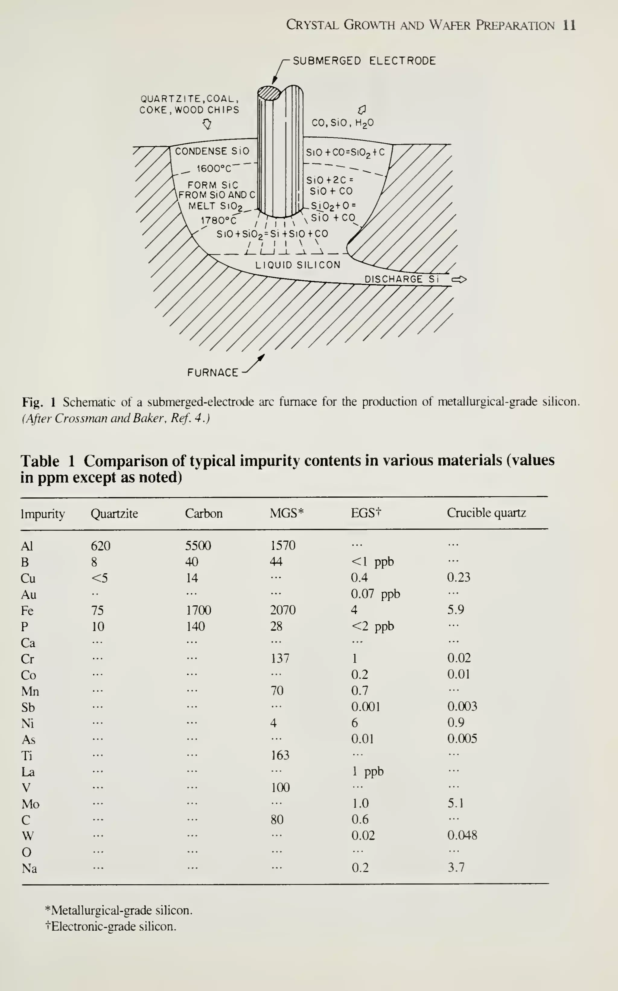
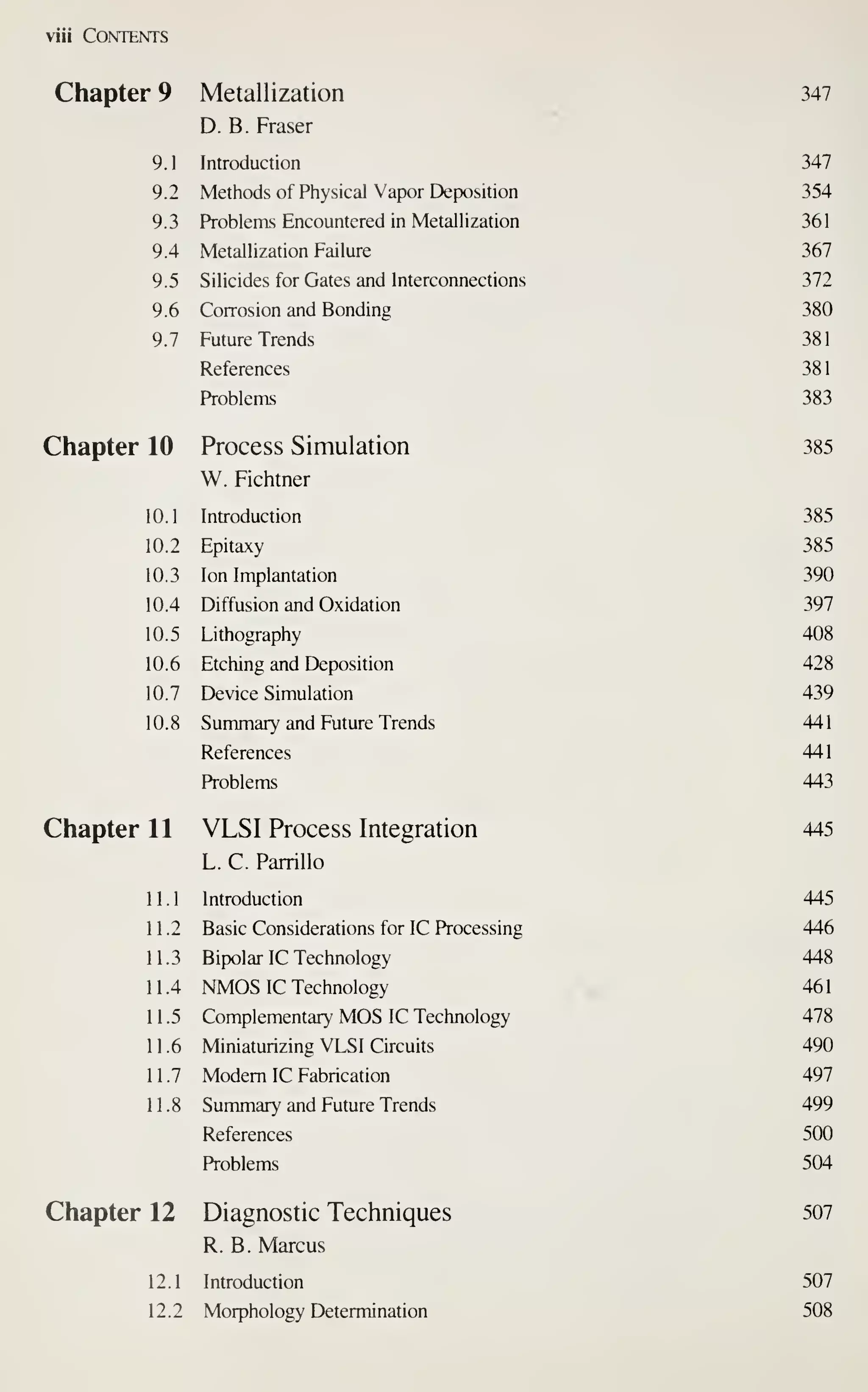
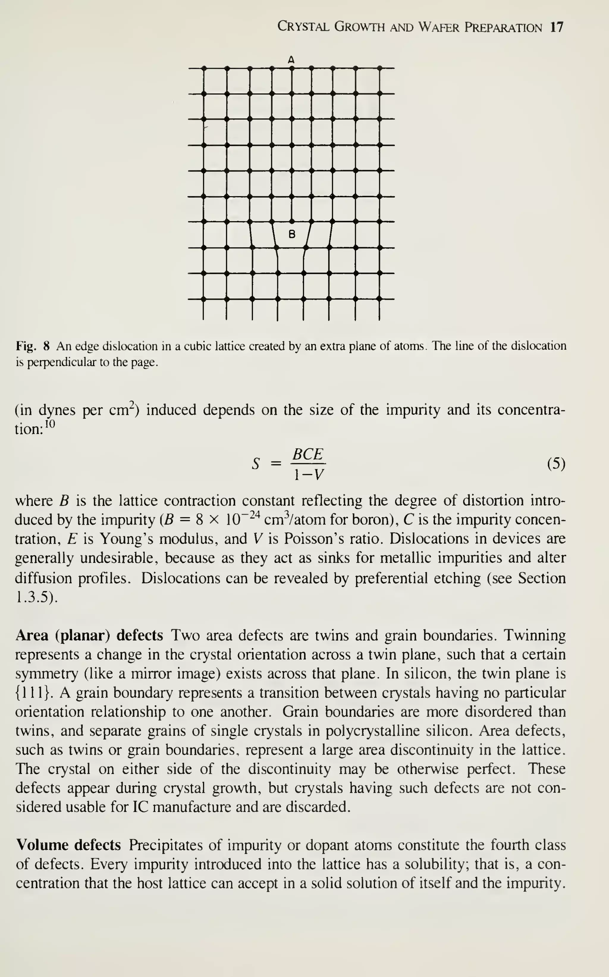
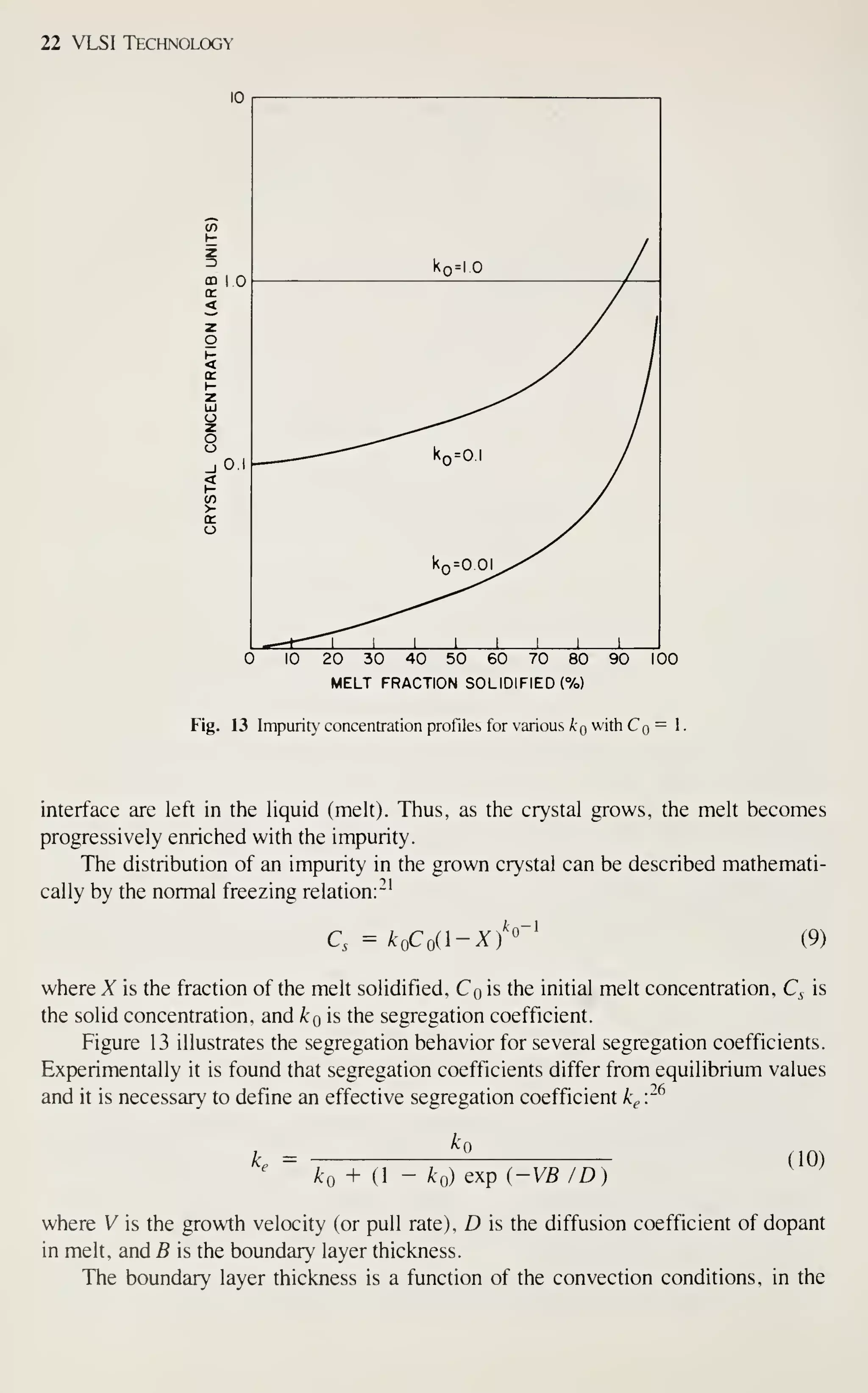
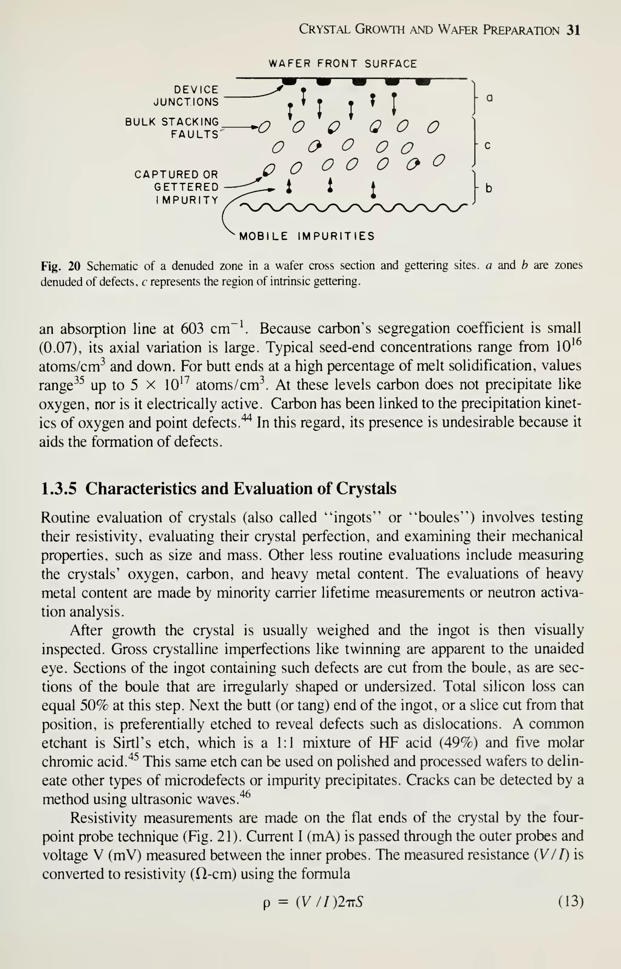
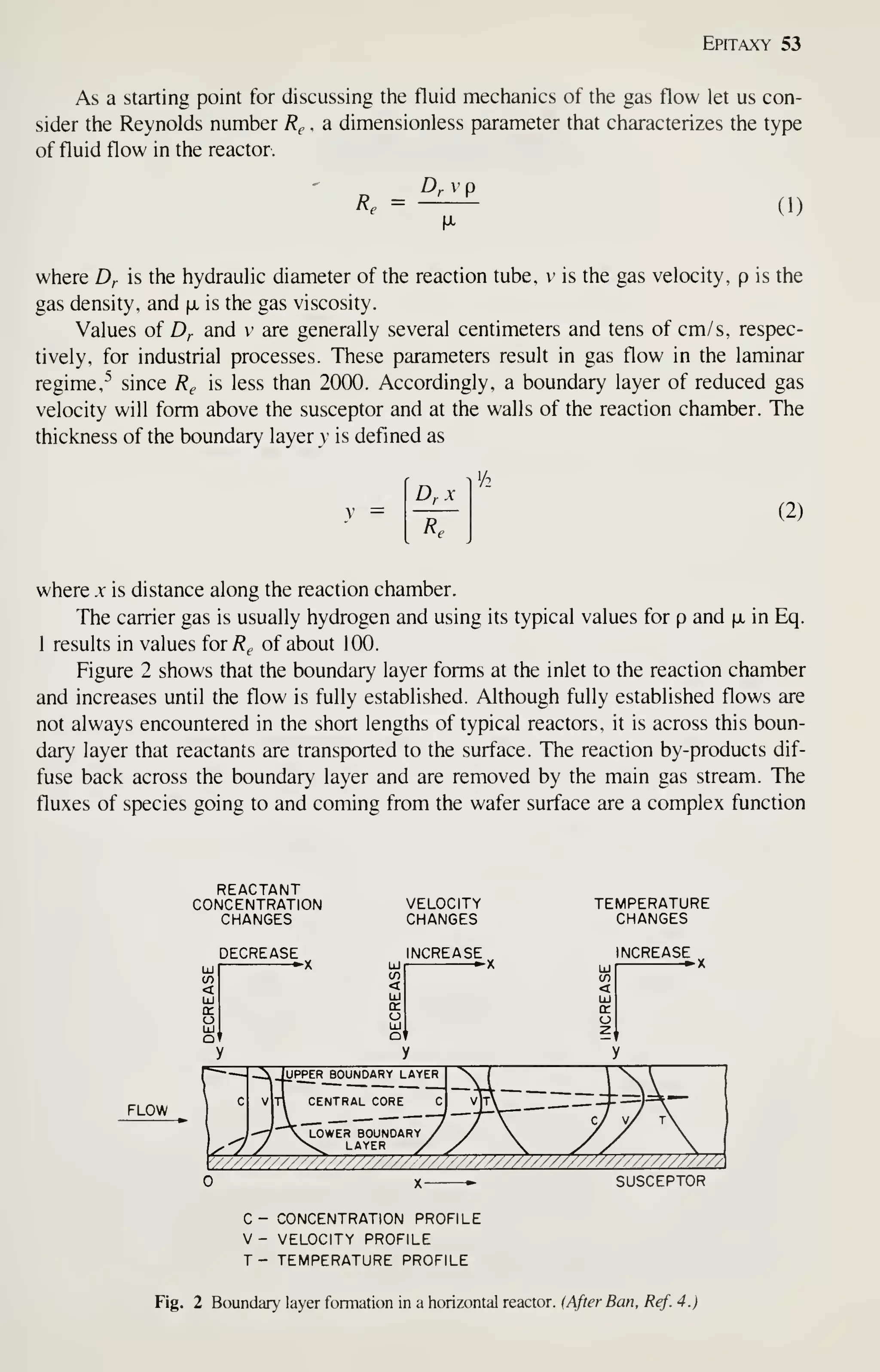
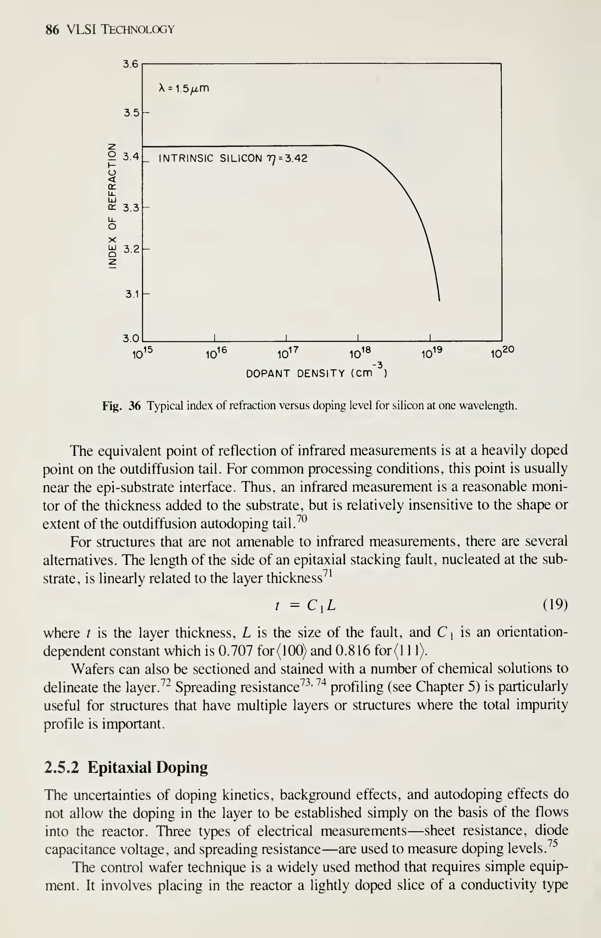
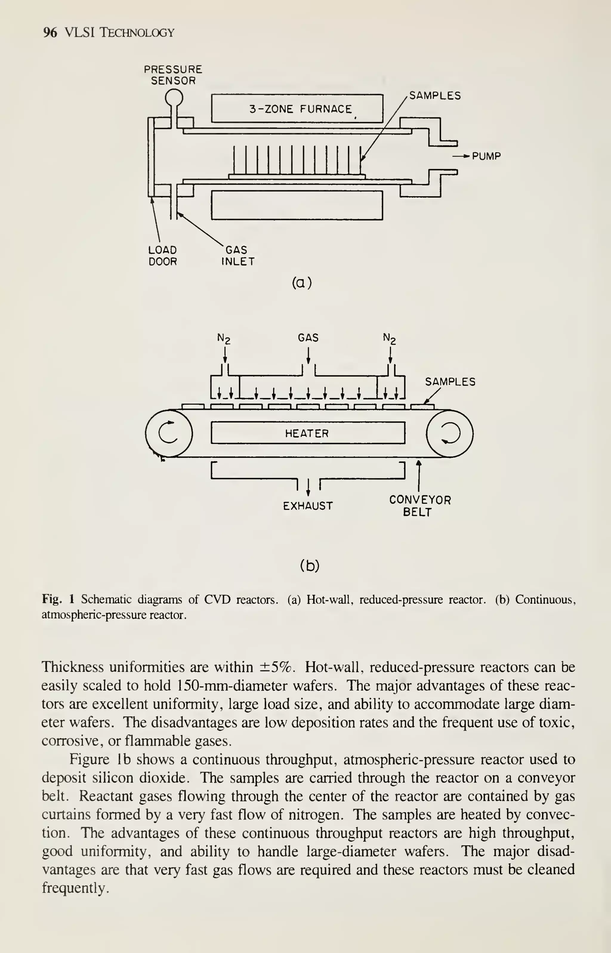
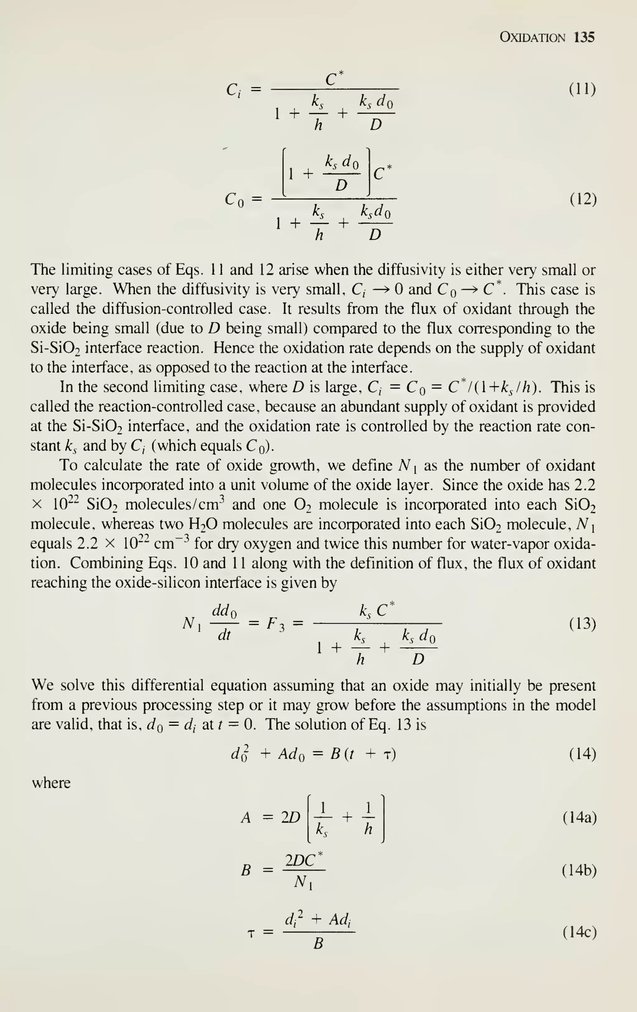
![CRYSTAL f
PLANE Ll
^
(100)
^[100] DIRECTION
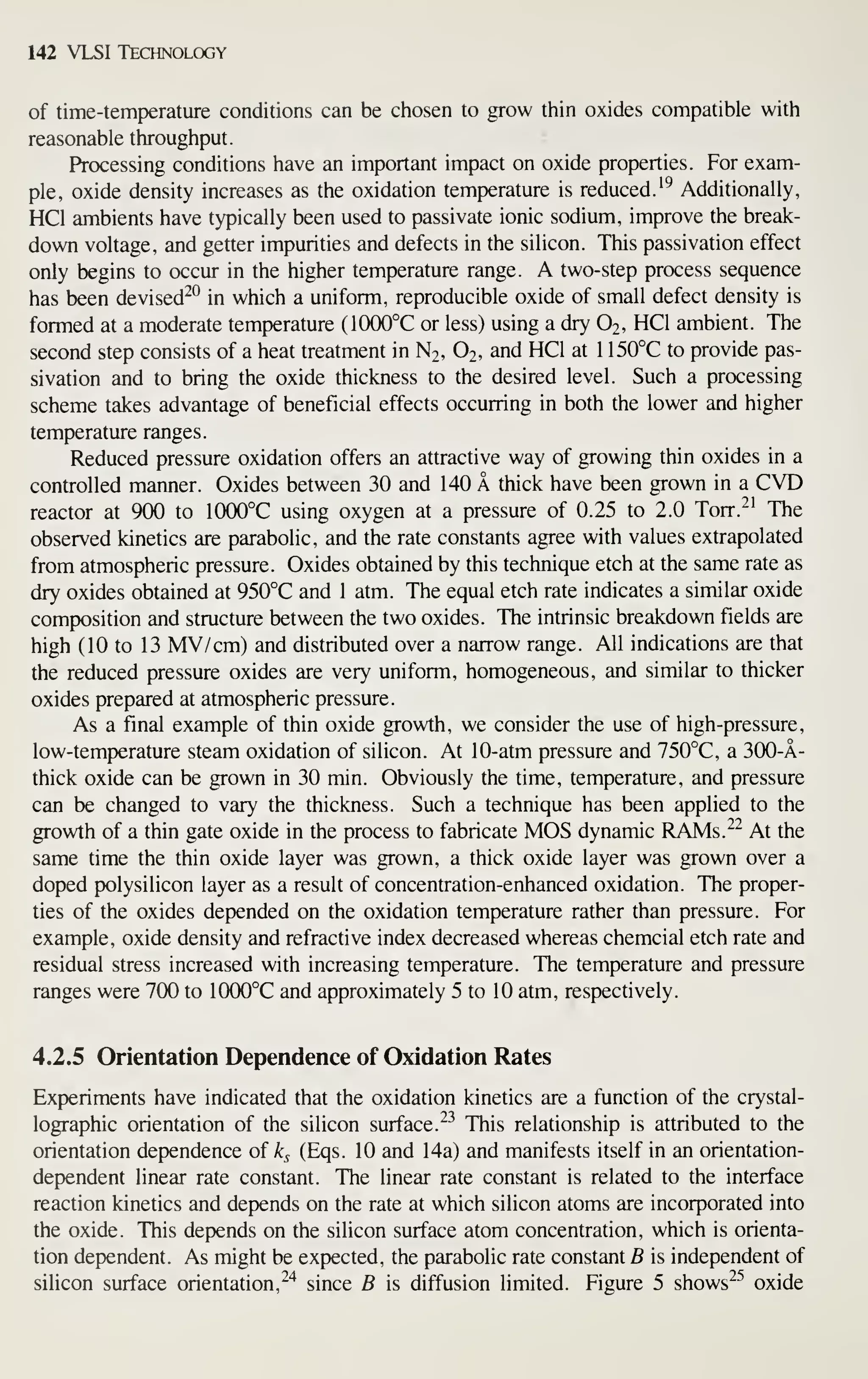
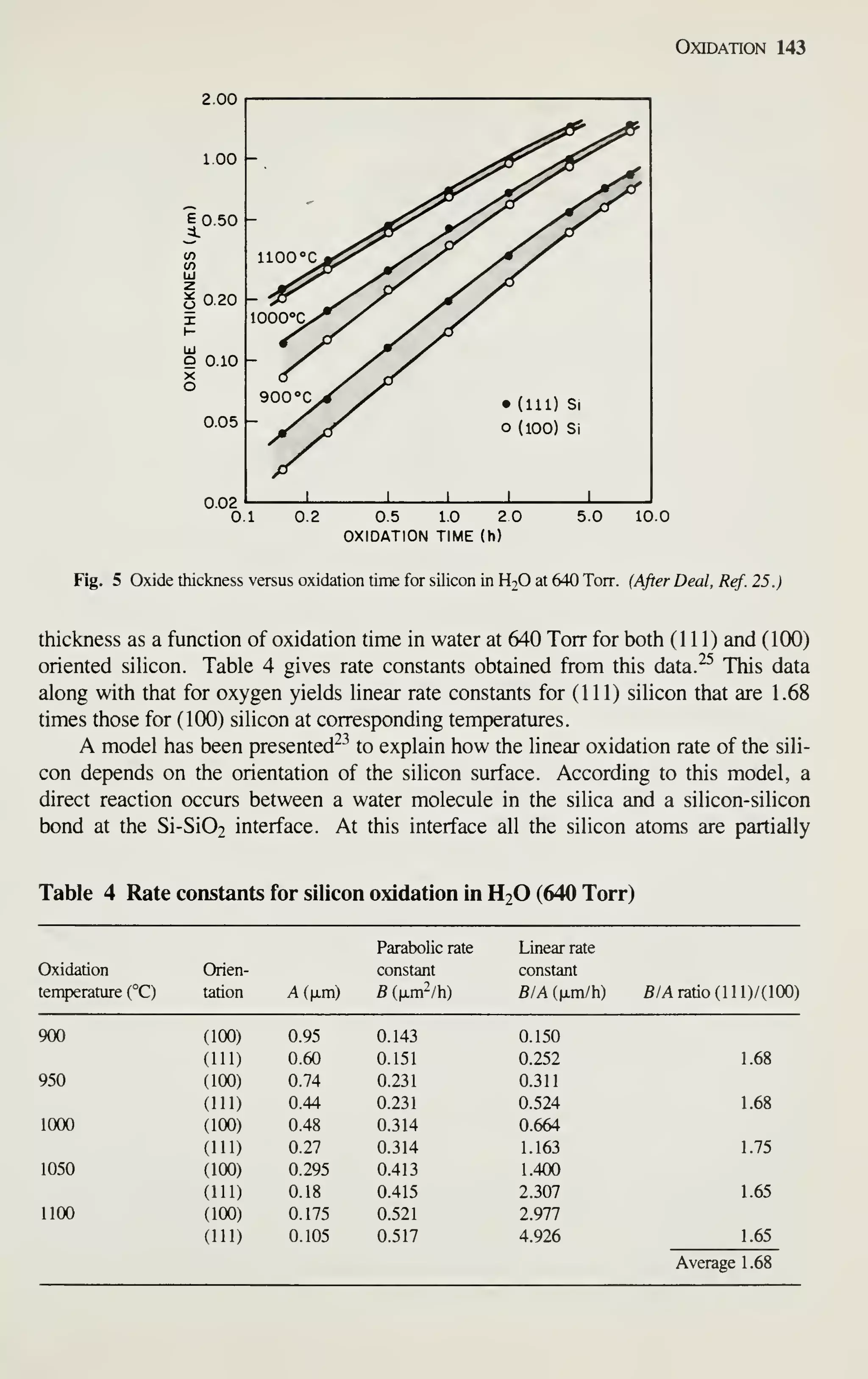
Crystal Growth and Wafer Preparation 15
1 ^
(110) (111)
Fig. 6 Schematic representation of Miller indices in a cubic lattice system.
example, [111] denotes a specific direction, whereas (1 1 1) denotes the family of all
eight directions equivalent to [111]. A (100) notation denotes a particular lattice
plane, and {100} denotes all the planes crystallographically equivalent of (100).
The processing characteristics and some material properties of silicon wafers
depend on the orientation. The {111} planes have the highest density of atoms on the
surface, so crystals grow most easily on these planes. Mechanical properties such as
tensile strength are highest for (1 1 1) directions. The moduli of elasticity also show an
orientation dependence (Appendix A). Processing characteristics such as oxidation are
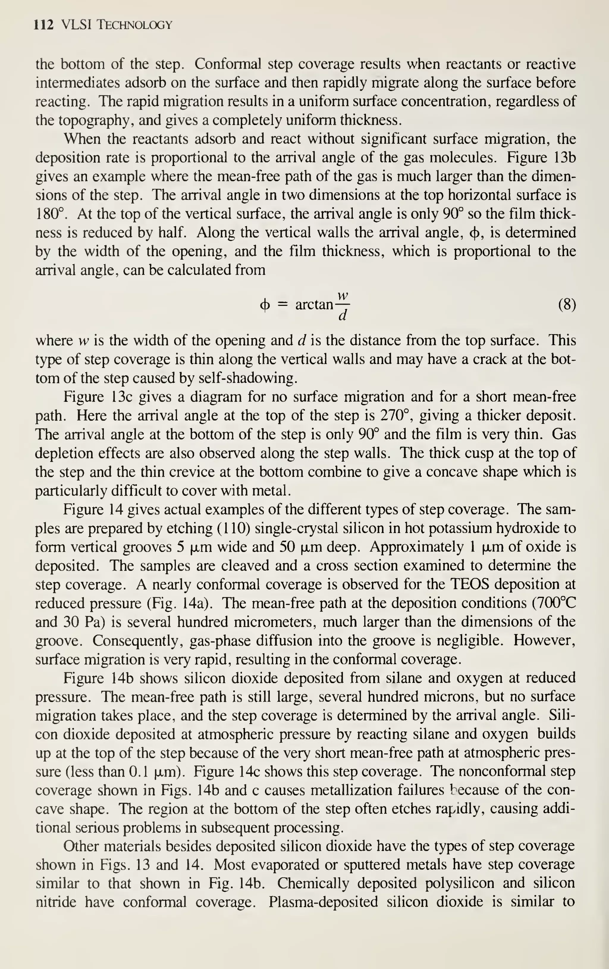
similarly orientation dependent. For example, {111} planes oxidize faster than {100}
planes, because they have more atoms per unit surface area available for the oxidation
reaction to occur. The choice of crystal orientation, therefore, is generally not left to
the discretion of the crystal grower, but is a device design consideration. Historically,
bipolar circuits have preferred (1 1 1) oriented material and MOS devices (100). There
are, of course, exceptions. Growth on other orientations such as (110) has been
demonstrated, but is more difficult to achieve routinely.^
A real crystal, as represented by a silicon wafer, differs from the mathematically
ideal crystal in several respects. It is finite, not infinite; thus, surface atoms are
incompletely bonded. The atoms are displaced from their ideal locations by thermal
agitation. Most importantly, real crystals have defects'^' " classified as follows: (1)
point defect, (2) line defect, (3) area or planar defect, and (4) volume defect. Defects
influence the optical, electrical, and mechanical properties of silicon.
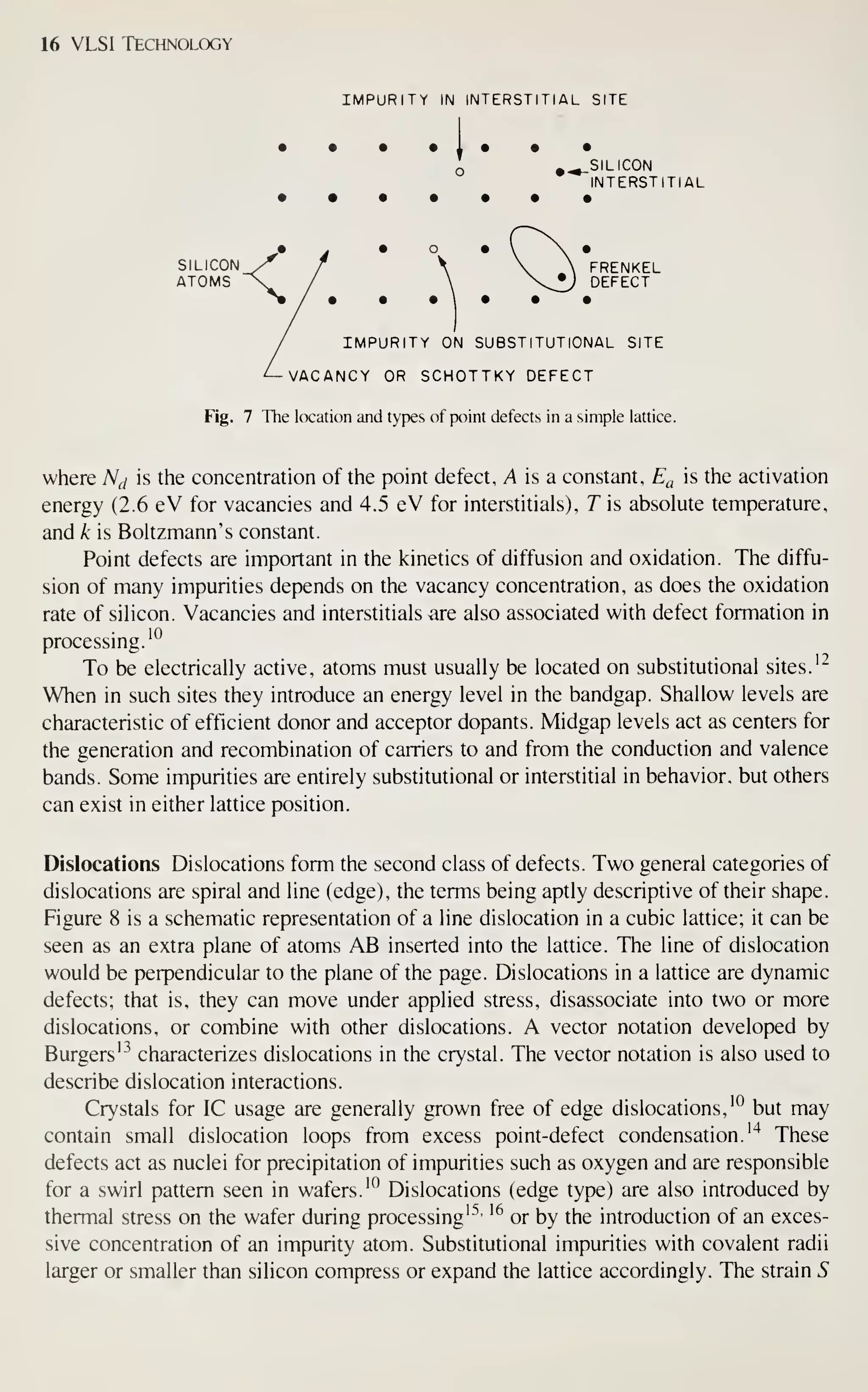
Point defects Point defects take several forms as shown in Fig. 7. Any nonsilicon
atom incorporated into the lattice at either a substitutional or interstitial site is con-
sidered a point defect. This is true whether the atom is an intentional dopant or unin-
tentional impurity. Missing atoms create a vacancy in the lattice called a "Schottky
defect," which is also considered a point defect. A silicon atom in an interstitial lat-
tice site with an associated vacancy is called a "Frenkel defect." Vacancies and inter-
stitials have equilibrium concentrations that depend on temperature. From thermo-
dynamic principles the concentration as a function of temperature can be derived and
has the following relation:
N^ = A exp {-EJkT) (4)](https://image.slidesharecdn.com/simonm-220913174129-44ec6f82/75/Simon-M-Sze-editor-Very-Large-Scale-Integration-VLSI-Technology-McGraw-Hill-Inc-US-1983-pdf-35-2048.jpg)
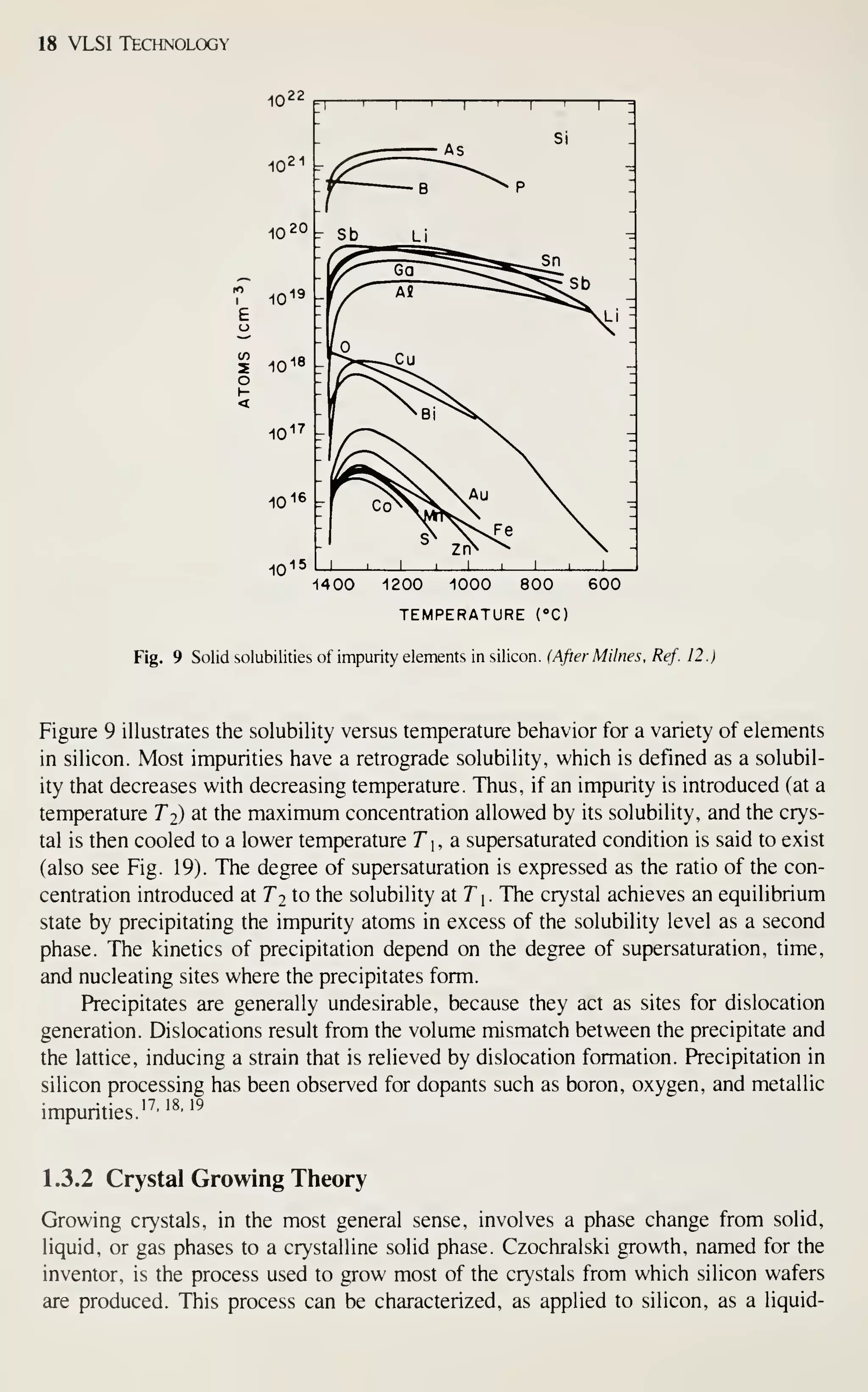
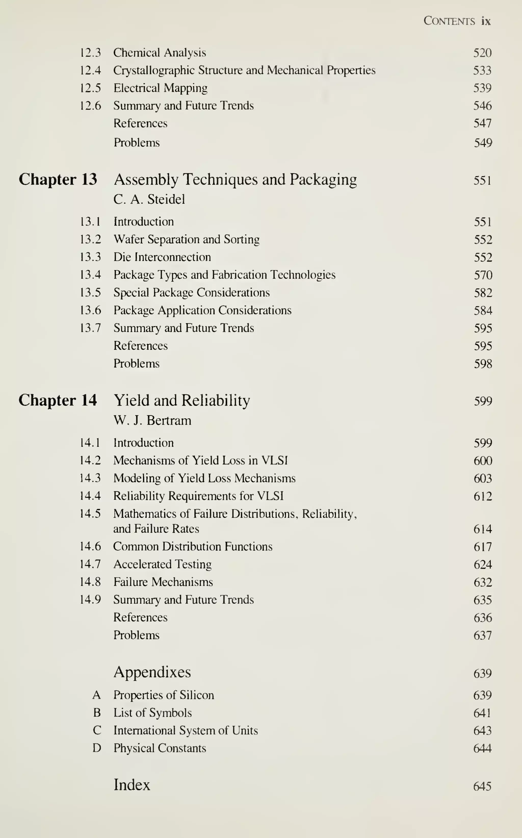
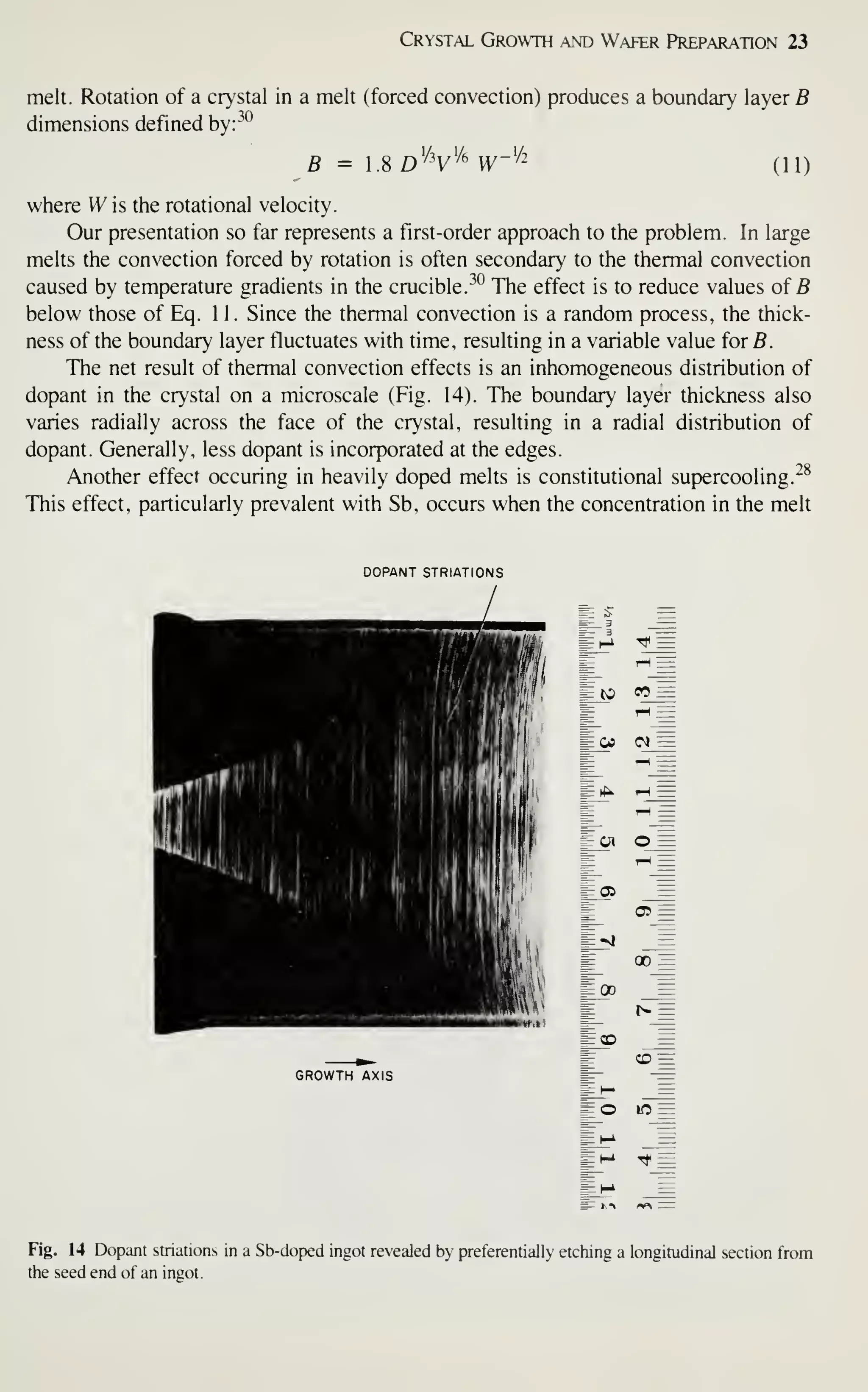
![Crystal Growth and Wafer Preparation 19
interface boundary layer (liquid)
SOLID (CRYSTAL)
GROWTH
AXIS
MP
o IMPURITY ATOMS
• SILICON ATOMS
DISTANCE
Fig. 10 Temperature gradients, solidification, and transport phenomena involved in Czochralski growth.
Positions 1 and 2 represent the location of isotherms associated with Eq. 6 and the crystal solidification at
the interface. Impurity atoms are transported across the boundary' layer and incorporated into the growing
crystal interface. M. P. is the melting point.
solid monocomponent growth system. This section discusses some elements of this
process as it relates to the understanding of the properties of the grown crystals. For a
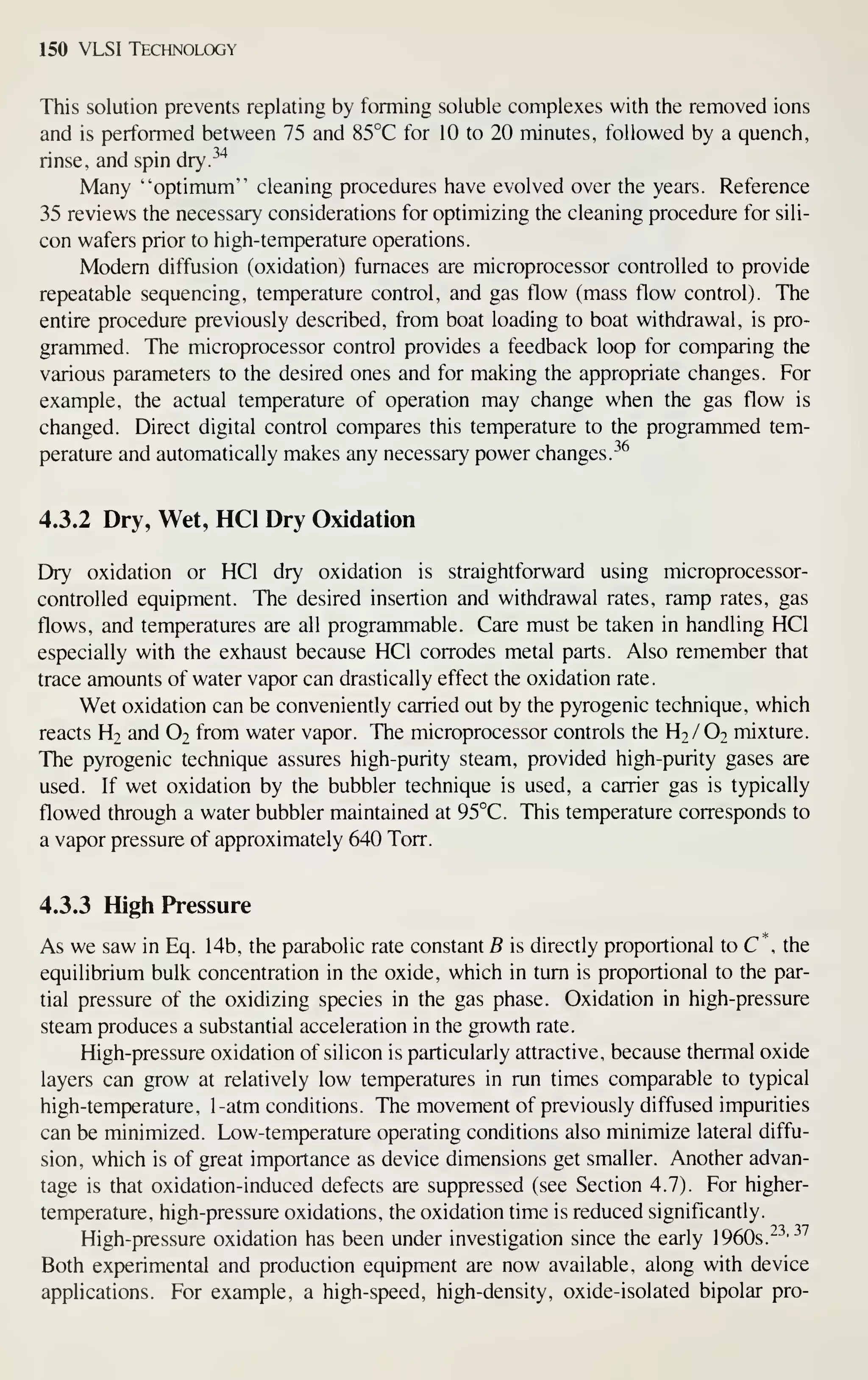
more complete treatment of crystal growth, refer to the many excellent books devoted
to the subject.^-
-^•-'
The growth of a CZ crystal involves the solidification of atoms from a liquid
phase at an interface. The speed of growth is determined by the number of sites on the
face of the crystal and the specifics of heat transfer at the interface. Figure 10
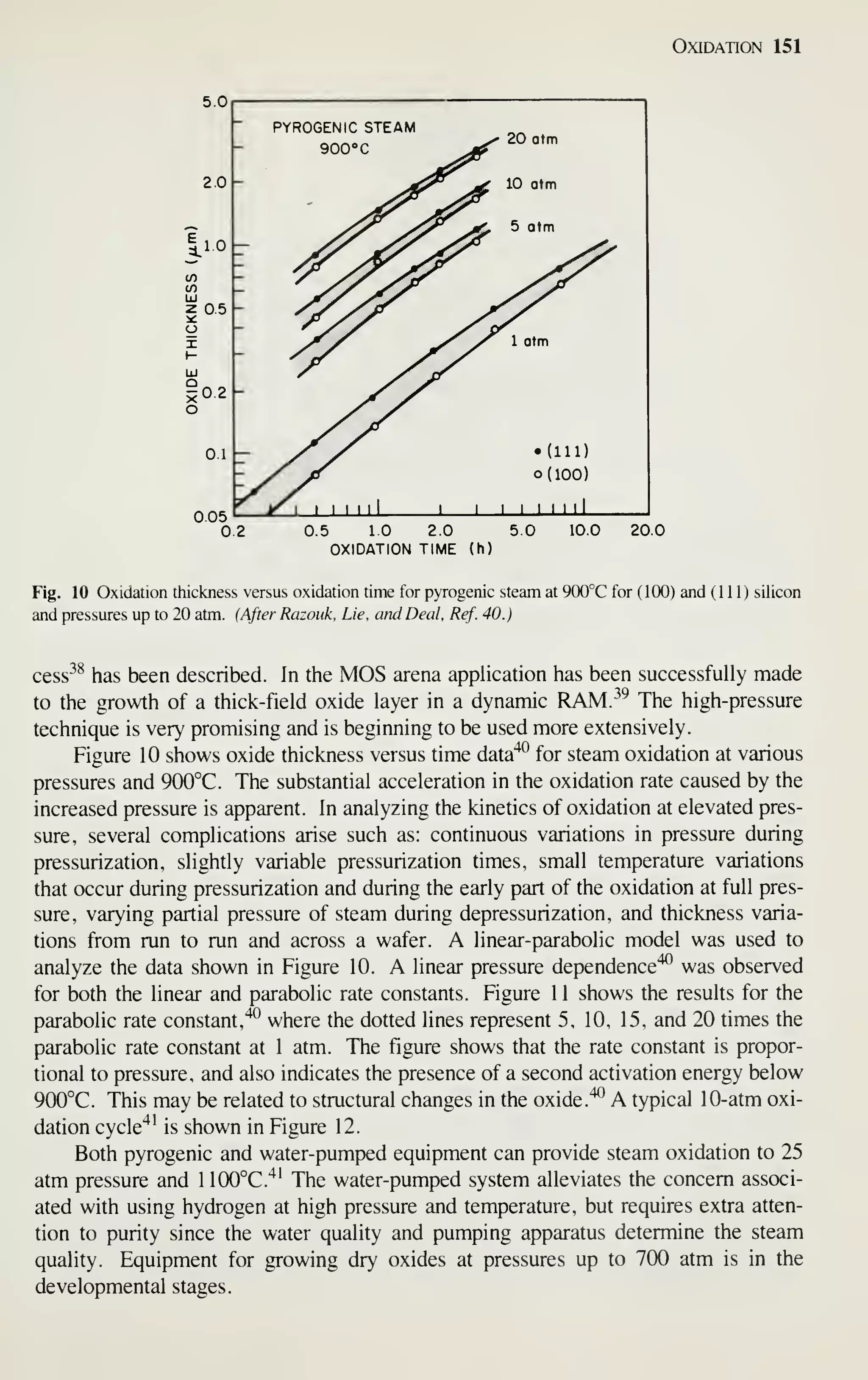
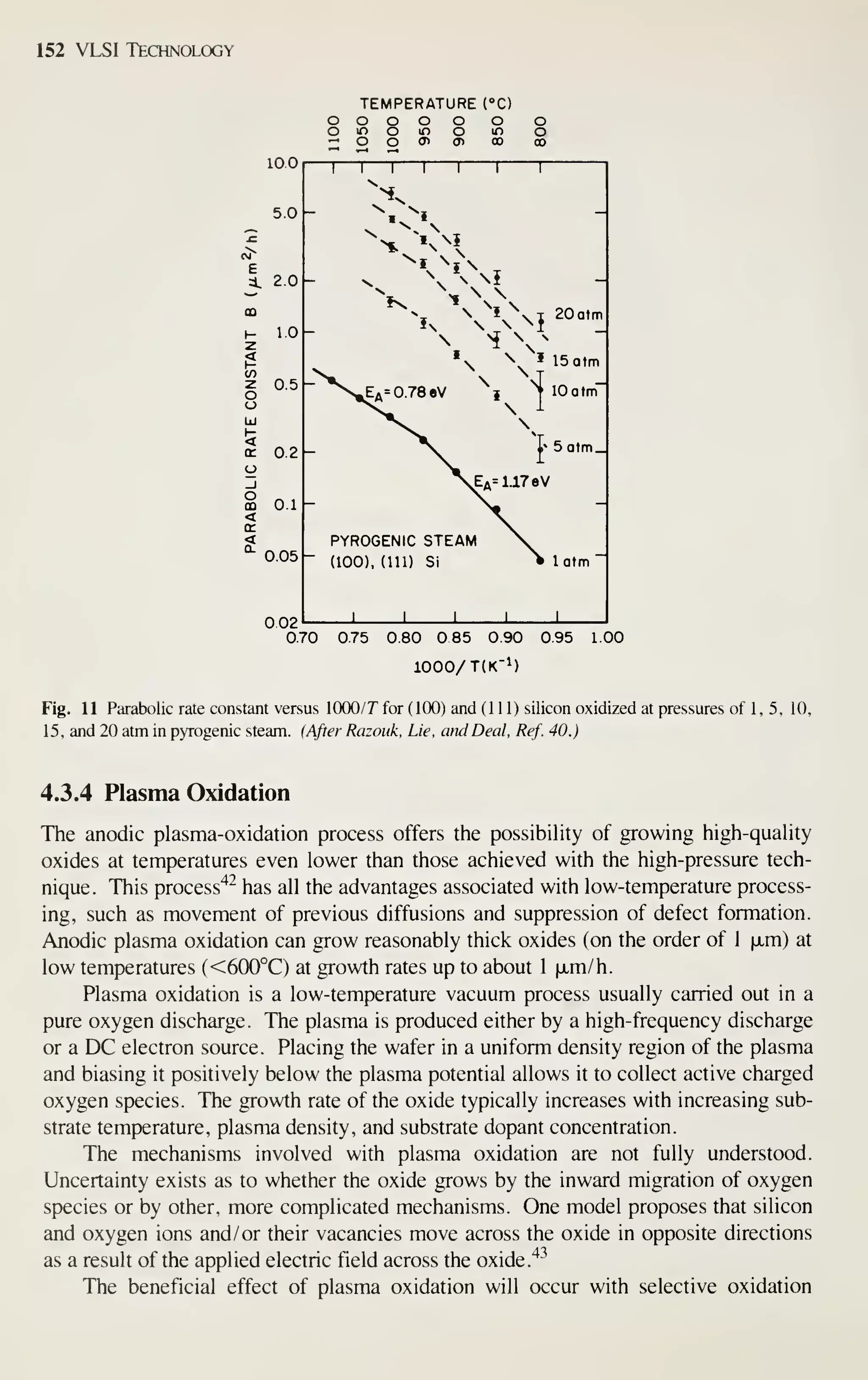
schematically represents the transport process and temperature gradients involved.
Macroscopically, the heat transfer conditions about the interface can be modelled by
the following equation:^'
dm
dt
+ k,-— A
dX]
1
dT ,
dx-)
(6)
where L is the latent heat of fusion, dm/dt is the mass solidification rate, T is the
temperature, kj and k^ are the thermal conductivities of the liquid and solid, respec-
tively, dT/dx I and dT/dxi are the thermal gradients at points 1 and 2 (near the inter-
face in the liquid and solid, respectively), and A
and A 2 are the areas of the iso-
therms at positions 1 and 2, respectively.
From Eq. 6 the maximum pull rate of a crystal under the condition of zero ther-
mal gradient in the melt can be deduced: '' ^^
- A_ 4L
U dx
V, (7)
where V^.^ is the maximum pull rate (or pull speed) and d is the density of solid sili-
con. Figure 1 1 is an experimentally determined temperature variation along a crystal.](https://image.slidesharecdn.com/simonm-220913174129-44ec6f82/75/Simon-M-Sze-editor-Very-Large-Scale-Integration-VLSI-Technology-McGraw-Hill-Inc-US-1983-pdf-39-2048.jpg)
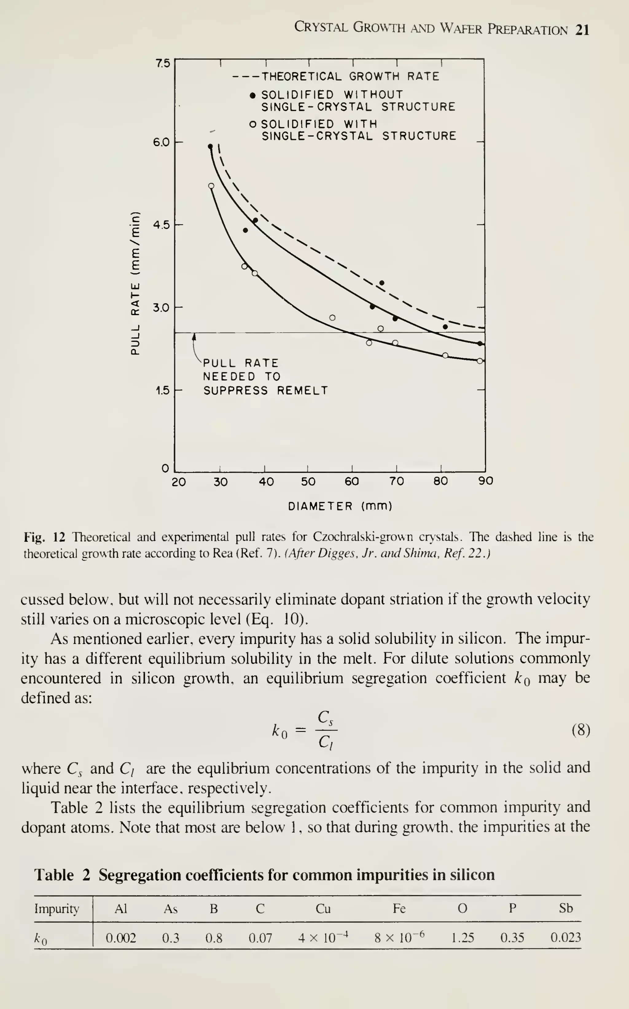
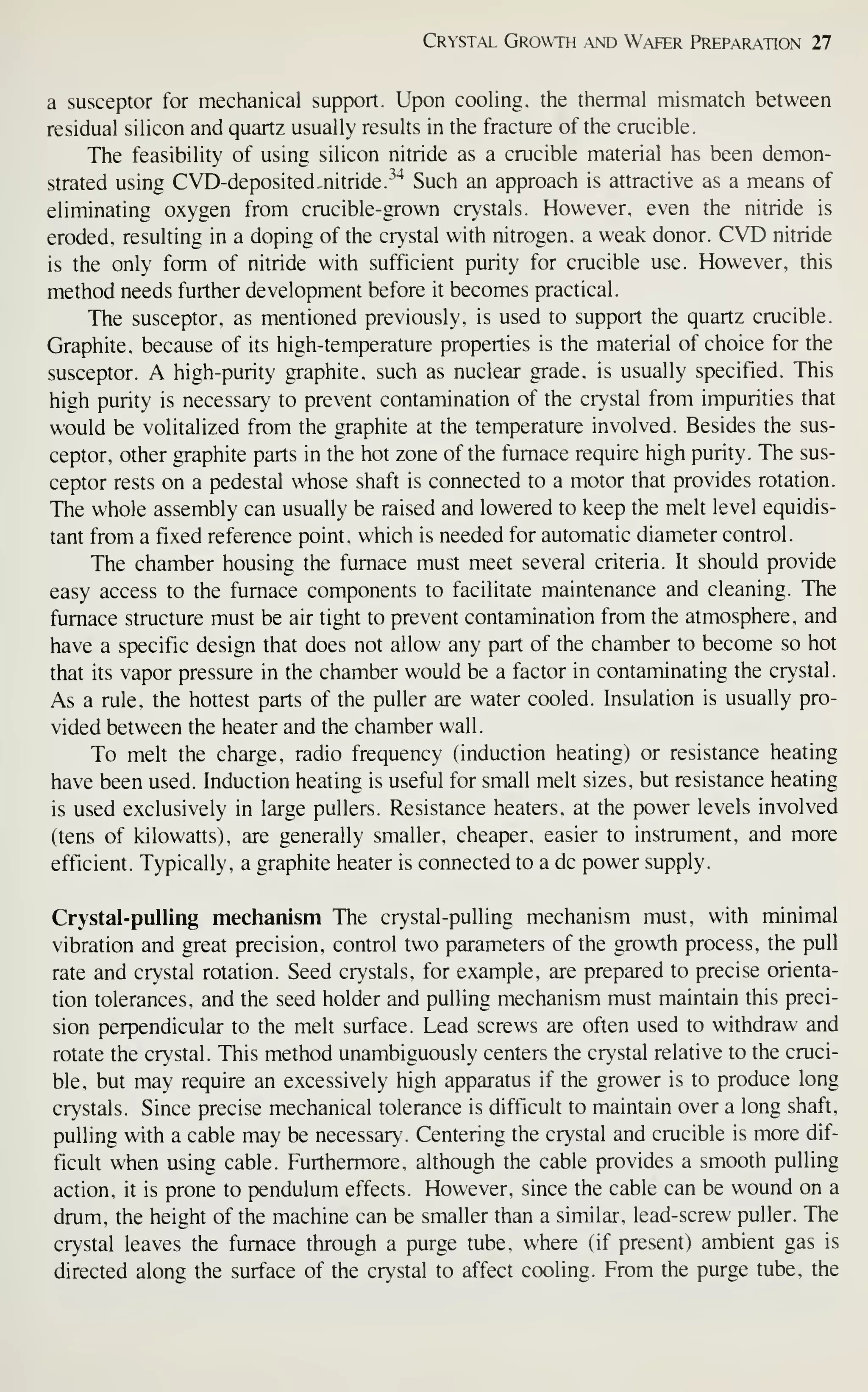
![Crystal Growth and Wafer Preparation 25
SEED SHAFT,
LIFT AND
ROTATION
SENSOR FOR
DIAMETER CONTROL
VIEW
PURGE
VPORT "^ T
TUBE I
^ ^
INSULATION-
HEATER
SUSCEPTOR
TEMPERATURE
SENSOR
"SUPPER HOUSING
CONTROL SYSTEM
AND
POWER SUPPLY
] ISOLATION VALVE
AMBIENT GAS INLET
SEED SHAFT a CHUCK
FURNACE CHAMBER
MELT
CRUCIBLE
EXHAUST
VACUUM
PUMP
CRUCIBLE ROTATION
AND LIFT
Fig. 16 Schematic representation of a crystal grower.
100-mm diameter and 3.0-m length. The puller has four subsystems as follows (Fig.
16):
1. Furnace: crucible, susceptor and rotation mechanism, heating element and
power supply, and chamber.
2. Crystal-pulling mechanism: seed shaft or chain, rotation mechanism, and seed
chuck.
3. Ambient control: gas source, flow control, purge tube, and exhaust or vacuum
system.
4. Control system: microprocessor, sensors, and outputs.
Furnace Perhaps the most important component of the growing system is the cruci-
ble (Fig. 3). Since it contains the melt, the crucible material should be chemically
unreactive with molten silicon. This is a major consideration, because the electrical
properties of silicon are sensitive to even ppb levels of impurities. Other desirable
characteristics for crucible material are a high melting point, thermal stability and
hardness. Additionally, the crucible should be inexpensive or reusable. Unfor-
tunately, molten silicon can dissolve virtually all commonly used high-temperature](https://image.slidesharecdn.com/simonm-220913174129-44ec6f82/75/Simon-M-Sze-editor-Very-Large-Scale-Integration-VLSI-Technology-McGraw-Hill-Inc-US-1983-pdf-45-2048.jpg)
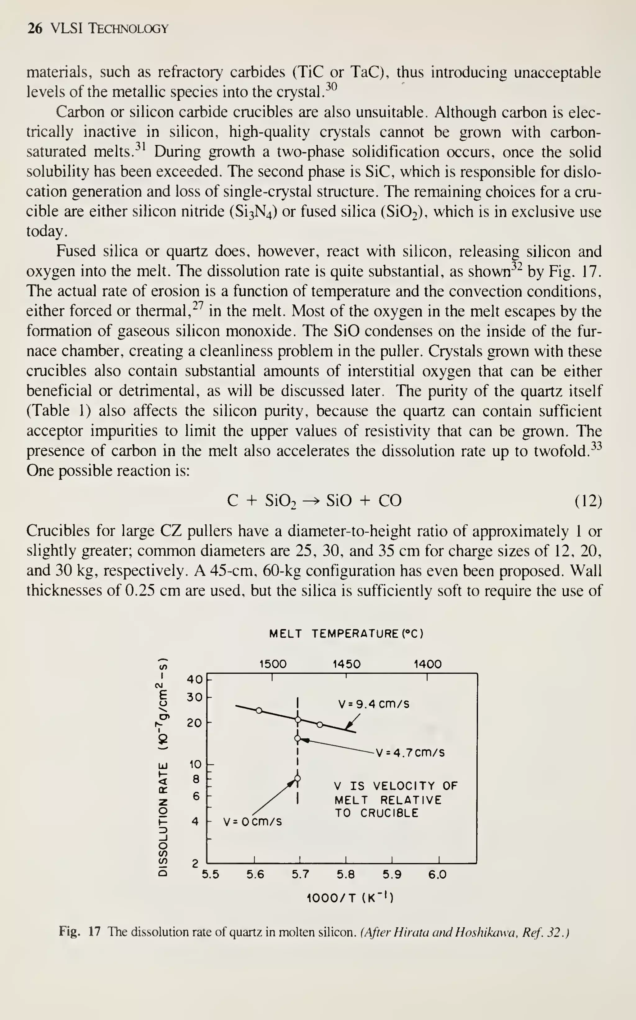
![Crystal Growth and Wafer Preparation 47
Large diameter wafers (>150 mm) are feasible and 200-mm wafers have been
produced. Practical implementation is awaiting the need for further productivity
improvements and improved circuit fabrication capability, particularly in the litho-
graphic area. Ingots of larger diameters will be grown in big pullers. The slower cool-
ing rates experienced by these such materials may alter the properties of the material,
particularly the point-defect kinetics. This topic provides an area for continued
research, because properties of the material are related to defects formed in device
processing, and thus related to IC yield.
REFERENCES
[1] C. L. Yaws, R. Lutwack, L. Dickens, and G. Hsiu, "Semiconductor Industry Silicon: Physical and
Thermodynamic Properties," Solid State TechnoL. 24, 87 ( 1981).
[2] J. C. Bailar, Editor, Comprehensive Inorganic Chemistry, 1, Pergamon Press, New York, 1973.
[3] W. Shockley, "The Theory of p-n Junctions in Semiconductors and p-n Junction Transistors," Bell
Syst. Tech. J., 28, 435 {949).
[4] L. D. Grossman and J. A. Baker, "Polysilicon Technology," Semiconductor Silicon 1977. Electro-
chem. Soc., Pennington, New Jersey, 1977, p. 18.
[5] Am. Soc. Test. Mater., ASTM Standard, F574, Part 43.
[6] W. Dietze, L. P. Hunt, and D. H. Sawyer, "The Preparation and Properties of CVD-Silicon Tubes
and Boats for Semiconductor Device Technology," J. Electrochem. Soc, 121 , 1112 (1974).
[7] S. N. Rea, "Gzochralski Silicon Pull Rate Limits," 7. Cryst. Growth, 54, 267 ( 1981).
[8] R. A. Laudise, The Growth of Single Crystals, Prentice Hall, Englewood Cliffs, New Jersey, 1970.
[9] L. D. Dyer, "Dislocation-Free Gzochralski Growth of (110) Silicon Crystals," J. Cryst. Growth, 47,
533(1979).
[10] K. V. Ravi, Imperfections and Impurities in Semiconductor Silicon. Wiley, New York, 198 1
.
[11] R. K. Watts, Point Defects in Crystals, Wiley and Sons, New York, 1977.
[12] A. G. Milnes, Deep Levels in Semiconductors. Wiley, New York, 1973.
[13] J. Friedel, Dislocations, Pergamon Press, New York, 1964.
[ 14] A. J. R. deKock and W. M. van de Wijgert. "The Effect of Doping on the Formation of Swirl Defects
in Dislocation-Free Gzochralski-Grown Silicon," J. Cryst. Growth, 49, 718 (1980).
[15] S. M. Hu, "Temperature Distribution and Stresses in Gircular Wafers in a Row during Radiative Cool-
ing," J. Appl. Phys., 40, 4413 ( 1969).
[16] K. G. Moerschel, C. W. Pearce, and R. E. Reusser, "A Study of the Effects of Oxygen Content, Ini-
tial Bow and Furnace Processing on Warpage of Three-Inch Diameter Silicon Wafers," Semiconductor
Silicon 1977, Electrochem. Soc, Pennington, New Jersey, 1977, p. 170.
[17] S. Kishino, Y. Matsushita, and M. Kanamori. "Carbon and Oxygen Role for Thermally Induced
IVIicrodefect Formation in Silicon," Appl. Phys. Lett.. 35, 213 ( 1979).
[18] A. Armigliato. D. Nobili. P. Ostoja, M. Servidori, and S. Solmi, "Solubility and Precipitation of
Boron in Silicon," Semiconductor Silicon 1977, Electrochem. Soc, Pennington, New Jersey, 1977,
p. 638.
[19] W. T. Stacy, D. F. Allison, and T. C. Wu, "The Role of Metallic Impurities in the Formation of Haze
Defects," Semiconductor Silicon 1981 , Electrochem. Soc, Pennington, New Jersey, 1981, p. 344.
[20] B. R. Pamplion, Crystal Growth, Pergamon Press. New York, 1983.
[21] W. R. Runyan, Silicon Semiconductor Technology, McGraw-Hill, New York, 1965.
[22] T. G. Digges, Jr. and R. Shima, "The Effect of Growth Rate, Diameter and Impurity Concentration
on Structure." J. Cryst. Growth, 50, 865 (1980).
[23] S. M. J. G. Van Run, "A Critical Pulling Rate for Remelt Suppression in Silicon Crystal Growth," J.
Cryst. Growth, 53, 441 (98).
[24] H. Kolker, "The Behavior of Nonrotational Striations in Silicon," J. Cryst. Growth, 50, 852 (1980).](https://image.slidesharecdn.com/simonm-220913174129-44ec6f82/75/Simon-M-Sze-editor-Very-Large-Scale-Integration-VLSI-Technology-McGraw-Hill-Inc-US-1983-pdf-67-2048.jpg)
![48 VLSI Technology
[25] J. Chikawa and S. Yoshikawa, "Swirl Defects in Silicon Single Crystals," Solid State TechnoL, 23,
65(1980).
[26] J. A. Burton, R. C. Prim, and P. Slichter.y. Chem. Phys.. 21, 1987 (1953).
[27] J. R. Carruthers, A. F. Win, and R. E. Reusser, "Czochralski Growth of Large Diameter Silicon Cry-
stals - Convection and Segregation," Semiconductor Silicon 1977, Electrochem. Soc., Pennington,
New Jersey, 1977, p. 61
.
[28] K. M. Kim, "Interface Morphological Instability in Czochralski Silicon Crystal Growth from Heavily
Sb-Doped Melt," 7. Electrochem. Soc, 126, 875 ( 1979).
[29] K. E. Benson, ,V. Lin, and E. P. Martin, "Fundamental Aspects of Czochralski Silicon-Crystal
Growth for VLSI," Semiconductor Silicon 1981, Electrochem. Soc., Pennington, New Jersey, 1981,
p. 33.
[30] M. H. Liepold, T. P. O'Donnell, and M. A. Hagan, "Materials of Construction for Silicon Crystal
Growth," J. Crysi. Growth, 40, 366 (1980).
[31] F. A. Voltmer and F. A. Padovani, "The Carbon-Silicon Phase Diagram for Dilute Carbon Concentra-
tion," Semiconductor Silicon 1973, Electrochem. Soc., Pennington, New Jersey, 1973, p. 75.
[32] H. Hirata and K. Hoshikawa, "The Dissolution Rate of Silica in Molten Silicon," Jpn. J. Appl. Phys.,
19, 1573(1980).
[33] B. Bathey, H. E. Bates, and M. Cretella, "Effect of Carbon on the Dissolution of Fused Silica in
Liquid Silicon," J. Electrochem. Soc, 128, 771 (1980).
[34] M. Watanabe, T. Usami, H. Muroaka, S. Matsuo, Y. Imanishi, and H. Nagashima, "Oxygen-Free
Silicon Single Crystal from Silicon-Nitride Crucible," Semiconductor Silicon 1981, Electrochem.
Soc., Pennington, New Jersey, 1981, p. 126.
[35] H. M. Liaw, "Oxygen and Carbon in Czochralski-Grown Silicon," Semicon. Int., 2,1( 1979).
[36] T. Carlberg, T. B. King, and A. F. Witt, "Dynamic Oxygen Equilibrium in Silicon Melts during Cry-
stal Growth," 7. f/mrof/zt'm. 5oc., 127, 189(1981).
[37] T. Suzuki, N. Isawa, Y. Okubo, and K. Hoshi, "CZ Silicon Growth in a Transverse Magnetic Field,"
Semiconductor Silicon 1981 , Electrochem. Soc., Pennington, New Jersey, 1981, p. 90.
[38] J. R. Patel, "Oxygen in Silicon," Semiconductor Silicon 1977. Electrochem. Soc., Pennington, New
Jersey, 1977, p. 521.
[39] Am. Soc. Test. Mater., ASTM Standard, F121-76, Part 43.
[40] J. Doerschel and F. G. Kirscht, "Differences in Plastic Deformation Behavior of CZ and FZ Grown
Silicon Crystals," Phys. Status SolidiA, 64, K85 (1981).
[41] K. Sumino et al., "The Origin of the Difference in the Mechanical Strengths of Czochralski Silicon,"
Jpn. J. Appl. Phys., 19, L49 (1980).
[42] C. W. Pearce, L. E. Katz, and T. E. Seidel, "Considerations Regarding Gettering in Integrated Cir-
cuits," Semiconductor Silicon 1981 , Electrochem. Soc., Pennington, New Jersey. 1981, p. 705.
[43] T. Nozaki, "Concentration and Behavior of Carbon in Semiconductor Silicon," J. Electrochem. Soc,
117, 1566(1970).
[44] Y. Matsushita, S. Kishino, and M. Kanamori, "A Study of Thermally Induced Microdefects in
Czochralski-Grown Silicon Crystals: Dependence on Annealing Temperature and Starting Material,"
Jpn. J. Appl. Phys., 19, LlOl (1980).
[45] D. G. Schimmel, "A Comparison of Chemical Etches for Revealing (100) Silicon Crystal Defects," J.
Electrochem. Soc, 123, 734 (1976).
[46] A. C. Bonora, "Silicon Wafer Process Technology: Slicing, Etching, Polishing," Semiconductor Sili-
con 1977, Electrochem. Soc., Pennington, New Jersey, 1977, p. 154.
[47] Am. Soc. Test. Mater., ASTM Standard, F84, Part 43.
[48] Am. Soc. Test. Mater., ASTM Standard, F723, Part 43.
[49] W. R. Thurber, R. L. Mattis, and Y. M. Liu, "Resistivity Dopant Density Relationship for Silicon,"
Semiconductor Characterization Techniques, Electrochem. Soc., Pennington, New Jersey, 1978,
p. 81.
[50] S. E. Bradshaw and J. Goorissin, "Silicon for Electronic Devices," J. Cryst. Growth, 48, 514
(1980).
[51] R. B. Hening, "Silicon Wafer Technology - State of the Art 1976," Solid State Technol., 19, 37
(1976).](https://image.slidesharecdn.com/simonm-220913174129-44ec6f82/75/Simon-M-Sze-editor-Very-Large-Scale-Integration-VLSI-Technology-McGraw-Hill-Inc-US-1983-pdf-68-2048.jpg)
![Crystal Growth and Wafer Preparation 49
[52] Semiconductor Equipment and Materials Institute (SEMI), Mountain View, California.
[53] The American Society for Testing and Materials (ASTM), Committee F-1 on Electronics, Philadel-
phia, Pennsylvania.
[54] H. Robbins and B. Schwartz, "Chemical Etching of Silicon," J. Electrochem. Soc, 106, 505 (1959);
107, 108(1960); 108, 365 (196ir; and 123, 1909(1976).
[55] W. Kern, "The Chemical Etching of Semiconductors," RCA Rev., 39, 278 (1978).
[56] I. Barycka, H, Teterycz, and Z. Znamirowski, "Sodium Hydroxide Solution Shows Selective Etching
of Boron-Doped Silicon," J. Electrochem. Soc. 126, 345 (1979).
[57] W. A. Baylies, "A Review of Flatness Effects in Microlithographic Technology," Solid State Tech-
noi.lA. 132(1981).
[58] A. C. Bonara, "Flex-Mount Polishing of Silicon Wafers," Solid State Technol.. 20, 55 ( 1977).
[59] C. W. Pearce and V. J. Zaleckas, "A New Approach to Lattice Damage Gettering," J. Electrochem.
Soc, 126, 1436(1979).
[60] K. Yamamoto, S. Kishino, Y. Matsushita, and T. Lizuka, "Lifetime Improvement in Czochralski-
Grown Silicon Wafers by the Use of aTwo Step Annealing," .4/7/?/. Phys. Lett., 36, 195 (1980).
[61] L. E. Katz, C. W. Pearce, and P. F. Schmidt, "Neutron Activation Study of a Gettering Treament for
CZSilkon Substrates," J. Electrochem. Soc, 128,620(1981).
[62] M. Ogino, T. Usami, and M. Watanabe, "Microdefects Due to Oxygen Precipitates and Their Appli-
cation to CMOS LSI and CCD Sensor," Electrochem. Soc. Extended Abstracts, 80-2, Abs. 435
(1980).
[63] B. Leroy and C. Plougoven, "Warpage of Silicon Wafers," J. Electrochem. Soc, 127, 961 (1980).
[64] P. F. Schmidt and C. W. Pearce, "A Neutron Activation Analysis Sttjdy of the Sources of Transistion
Group Metal Contamination in the Silicon Device Manufacturing Process," J. Electrochem. Soc,
128,630(1981).
PROBLEMS
1 Iron is an impurity in quartz crucibles. Using a concentration value of 2 x lO'^ /cnr' in the crucible,
assume 300 cm-' of the crucible is dissolved into a 6500-g melt, all at the beginning of the cycle. Calculate
the seed (0% solidified) and tang end (90% solidified) iron concentration in the ingot.
2 Using the equation governing crystal growth (Eq. 6), derive an expression relating growth rate inversely
to crystal diameter. Assume no temp)erature gradient in the melt. Since the heat flow down the crystal is
small, assume heat flow from the crystal is predominantly from radiation.
3 Calculate the number of gallons of HF and HNO3 acid needed to remove the work damage from 5000
wafers of 100-mm diameter.
4 The seed crystal used in CZ growing is usually "necked down" to a small diameter (3 mm) as a means to
initiate dislocation-free growth. Using the yield strength of silicon, calculate the maximum mass of silicon
that could be supported by such a seed. Convert this to a length for 100- and 1 25-mm-diameter crystals.
5 Large growers, such as that pictured in the chapter, require 120 kWh to convert a kilogram of polysilicon
into a crystal. Account for this energy in terms of the energy needed to melt the silicon, the radiation loss
fiom the melt surface, and conduction down the crystal. Is all the energy accounted for? Assume that a 10-
kg charge of polysilicon is used to grow a 10-cm-diameter crystal from a 25-cm-diameter crucible at a rate of
0.0025 cm/s.
6 Solar cells have been suggested as an alternative energy source. Conduct the following feasibility calcula-
tion: How much polysilicon would be required to supply all the United States' electrical needs from 100-
mm-diameter Czochralski-grown silicon wafers, and how much land area would this require? Compare the
silicon used to current consumption. Use the following data:
1
.
The average U.S. weekly power consumption is 42 x lO' kWh.
2. Assume that each gram of silicon in the finished cell required 5 g of polysilicon.
3. The average solar energy falling on the earth's surface is 1340 W/m"; assume 50 h of daylight per
week.
4. The cell will convert 8% of all incident energy to electrical power.](https://image.slidesharecdn.com/simonm-220913174129-44ec6f82/75/Simon-M-Sze-editor-Very-Large-Scale-Integration-VLSI-Technology-McGraw-Hill-Inc-US-1983-pdf-69-2048.jpg)

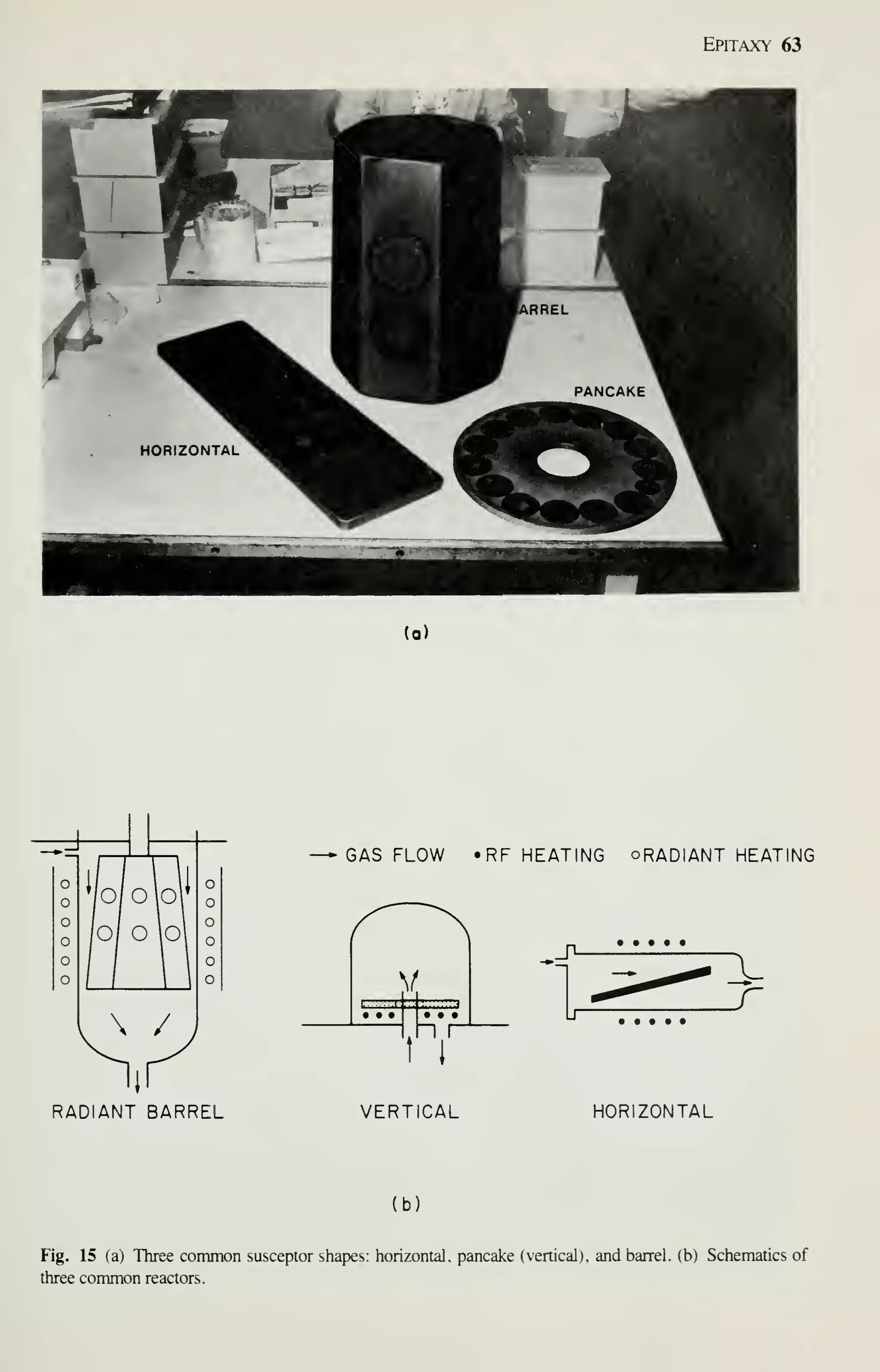
![68 VLSI Technology
As in oxidation, diffusion, and LPCVD processes, wafers are cleaned before the
expitaxy process begins. All organic and metallic residues on the wafers must be
removed.^^ Particles are removed by using ultrasonic agitation in the cleaning baths,
by brush scrubbing with water, or by high-pressure water jets. Clean wafers must be
handled carefully to prevent recontamination, especially by particles. To prevent par-
ticle contamination, the entire reactor or load station is usually installed in a clean
room. A second method is to use a clean-air hood at the loading station.
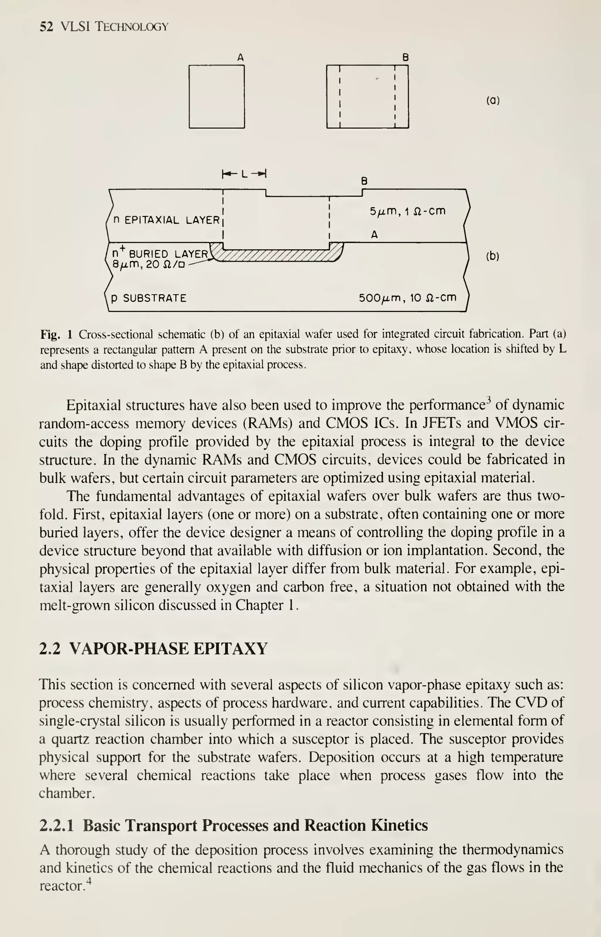
2.2.5 Buried Layers
To fabricate bipolar ICs, usually one or more diffusions are applied to the substrate to
create the necessary isolation, collector, emitter, or base functions (Fig. 1). These dif-
fusions are applied to the substrate prior to epitaxy using the lithographic, oxidation,
diffusion, or ion-implantation processes discussed in other chapters. The diffusions
are called buried layers or diffusions under film. The presence of a buried layer com-
plicates the epitaxial process because of its effect on autodoping (vertical and lateral),
defects, pattern shifting, and pattern distortion.
The pre-epitaxial process leaves a step of 500 to 1000 A around the perimeter of
the buried layer that marks its location (A of Fig. 1). Subsequent masking levels must
be properly aligned with the buried layer pattern. Unfortunately, the deposition pro-
cess shifts the pattern (B of Fig. lb). Lithographic masks must compensate for the
amount of the shift (L of Fig. lb). A separate but related effect is pattern distortion or
washout, which alters the shape of the feature in the layer. Figure la also illustrates
the nature of pattern distortion. The pattern in the epitaxial layer is thus misplaced and
15 -
o 10
•
o
DATA
INTERPOLATED
EPITAXIAL THICKNESS ( f^m)
-
15
-
13
-
^1
-
9
- 7
-
M/^''^
-
1 1 1
5 -
30 60
SURFACE ORIENTATION
[minutes of arc off <100>]
Fig. 17 Pattern shift for a (100) orientation with various amounts of misorientation. (A.fxer Drum and Clark,
Ref. 37.)](https://image.slidesharecdn.com/simonm-220913174129-44ec6f82/75/Simon-M-Sze-editor-Very-Large-Scale-Integration-VLSI-Technology-McGraw-Hill-Inc-US-1983-pdf-88-2048.jpg)
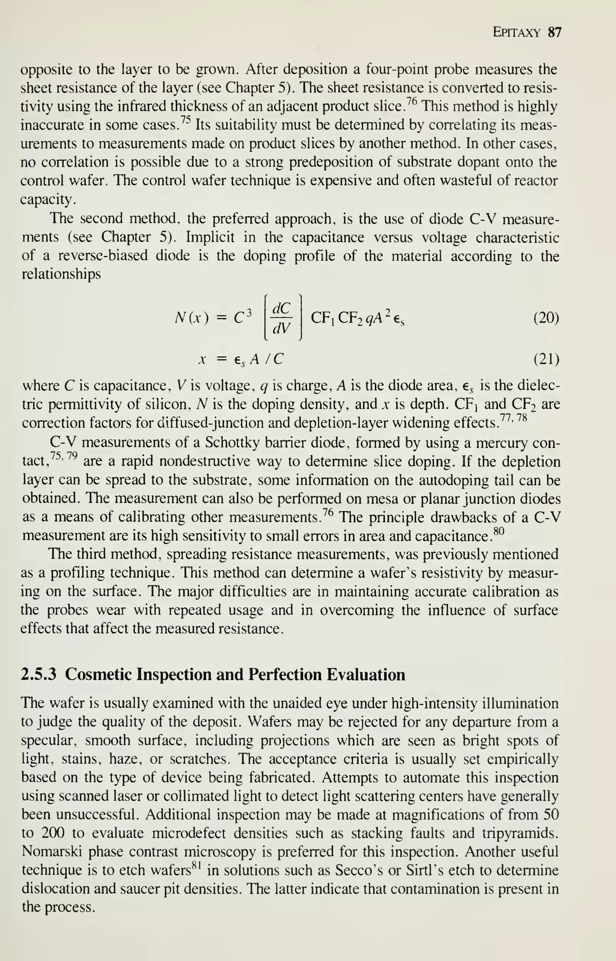
![Epitaxy 69
misshaped relative to its original configuration in the substrate. These effects place
limitations on the design of high-density circuits, and are a complicated function of
substrate orientation, growth rate and temperature, and silicon source.
^^
The crystal orientation has a profound effect on pattern shift.
-^^
Since the layer
does not grow normal to the substrate but rather by additions to microsteps (Fig. 9),
the macrostep marking the diffusion is shifted. As a result the microscopic growth
processes are altered by the orientation of the wafer. Current practice is to misorient
(1 1 1) wafers by 2 to 5° towards the nearest (1 10) direction and to orient (100) wafers
exactly on the orientation. Figure 17 illustrates the (100) case; note that the pattern
shift changes with epitaxial thickness. As shown in Fig. 18, pattern shift is indepen-
dent of reactor design, ^^^
but does show a pronounced dependence on growth rate and
VERTICAL GEOMETRY
ORIENTATION <111>
DEPOSITION RATE
o 1 0|im/min
5/j.m/min
/im/min
m /min
1000 1100 1200
3-
2-
1
-
0_
HORIZONTAL GEOMETRY
1000 1100 1200
3-
2-
cn 1 _
CYLINDRICAL GEOMETRY
1000 1100 1200
TRUE TEMPERATURE (°C)
- (a)
(b)
- (C)
Fig. 18 Pattern shift as a function of reactor [(a) vertical, (b) horizontal, and (c) cylindrical (or barrel)],
temperature, and growth rate. (After Lee etal., Ref. 38.)](https://image.slidesharecdn.com/simonm-220913174129-44ec6f82/75/Simon-M-Sze-editor-Very-Large-Scale-Integration-VLSI-Technology-McGraw-Hill-Inc-US-1983-pdf-89-2048.jpg)
![Epitaxy 81
106
105 -
103 —
10'
"1 I I I I
r I
I I
1
r
J I u
—
o
o-
_l I L.
10 20
PREHEAT TIME OF SUBSTRATE (min)
Fig. 30 The dependence of film quality on predeposition heating time. (After Sugiura and Yamaguchi, Ref.
53.)
CVl 10
E
GROWTH TEMPERATURE (°C)
6 800 700
'
1 1
1
1
600
ti- 10-
en
z
t 10^ I-
en
2
LlI
Q
Z
H 10^ -
<
o
o
_l
en
10'
E= 3.5 ev
^ll
'
I I I I I I I I I I I I I I 1 I I I I ] I 1
0.9 1.0 1.1
10^ /T(K)
Fig. 31 The dependence of film perfection on growth temperature. (After Sugiura and Yamaguchi, Ref.
53.)](https://image.slidesharecdn.com/simonm-220913174129-44ec6f82/75/Simon-M-Sze-editor-Very-Large-Scale-Integration-VLSI-Technology-McGraw-Hill-Inc-US-1983-pdf-101-2048.jpg)
![88 VLSI Technology
2.5.4 Lifetime
The lifetime of minority carriers is generally not a consideration in structures intended
for IC fabrication, but could be of interest in some devices such as dynamic RAMs.
Several measurements involving the transient response of diodes or MOS capacitors
are applicable to epitaxial layers.
^^'^-^
However, the diffusion length of carriers is
often many times that of the layer thickness. This complicates the interpretation of the
measurement results.
2.6 SUMMARY AND FUTURE TRENDS
Epitaxy as a process will remain integral to circuit manufacture. It offers doping pro-
files and material properties not obtainable otherwise. Homoepitaxial silicon struc-
tures will remain popular design choic in the foreseeable future. The advantages of
SOI technologies are compelling for h h-density and high-speed circuits. In particu-
lar, if silicon-on-Si02 can be perfected, it will offer the advantages of SOS without
the problems. Lateral-seeded SOI will undoubtedly receive considerable research
attention. MBE would be advantageous in fully ion-implanted VLSI circuits in which
the total thermal cycle is minimized so that the doping capabilities of MBE can be
exploited.
Although presently available equipment is adequate for most needs, several
aspects of the epitaxial process could be improved. In keeping with automation else-
where in the fabrication process, an autoloading epitaxial reactor remains a desirable
objective. This equipment could take the form of a cassette-fed machine processing a
single wafer at a time. Conceptually, a uniwafer reaction chamber could be optim-
ized for temperature and gas flows to produce wafers having exceptional uniformity.
The throughput of epitaxial reactors is less than that of LPCVD processes (Chapter 3)
by a factor of 5 to 10. However, monocrystalline silicon cannot be grown in LPCVD
equipment. One difficulty is the low growth rates in the usual LPCVD temperature
ranges (Fig. 8). An alternative reactor design, ^"^
termed the rotary disc, is similar in
load configuration to LPCVD equipment, and offers high capacity and efficiency.
Large-scale use of MBE will require equipment with throughputs comparable to
present-day epitaxial reactors.
Although epitaxial processes are well characterized and understood, the trend to
thinner layers for bipolar and unipolar ICs will result in incremental process improve-
ments and the continued study of autodoping effects. Additionally, contamination,
responsible for precipitates in epitaxial layers, needs to be reduced commensurate
with the requirements of VLSI devices. Contamination-free epitaxy will be a
worthwhile process improvement.
REFERENCES
[1] H. C. Theuerer et al., "Epitaxial Diffused Transistors," Proc. IRE. 48, 1642 (1960).
[2] F. E. Holmes and C. A. T. Salama, "VMOS—A New MOS Integrated Circuit Technology," Solid
State Electron . , 1 7 , 79 1 ( 1 974)
.
[3] D. S. Yaney and C. W. Pearce, "The Use of Thin Epitaxial Layers for MOS VLSI," Proceedings of
the 1981 International Electron Device Meeting , IEEE, 1981, p. 236.](https://image.slidesharecdn.com/simonm-220913174129-44ec6f82/75/Simon-M-Sze-editor-Very-Large-Scale-Integration-VLSI-Technology-McGraw-Hill-Inc-US-1983-pdf-108-2048.jpg)
![Epitaxy 91
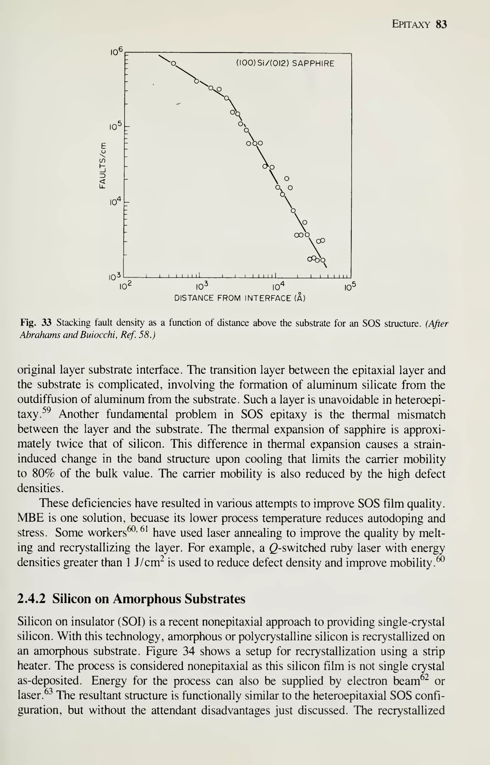
[58] M. S. Abrahams and C. J. Buiocchi, "Cross-Sectional Electron Microscopy of Silicon on Sapphire,"
Appl. Phys. Lett.. 27, 325 (1975).
H. Schlotter, "Interface Properties of Sapphire and Spinel." J. Vac. Sci. Technol.. 13, 29 (1976).
Y. Kobayaski. T. Suzuki, and M. Tamura. "Improvement of Crystalline Quality of SOS with Laser
hradiation Techniques." y/?«. J. Appl. Phys.. 20. L249 ( 1981).
G. A. Sai-Halar. F. F. Fang. T. O. Sedgwick, and A. Segmuller. "Stress-Relieved Regrowth of Sili-
con on Sapphire by Laser Annealing." Appl. Phys. Lett.. 36. 419 (1980).
K. Shibata. T. Inoue. and T. Takigawa. "Grain Growth of Polycr}'stalline Silicon Films on SiOi by
CW Scanning Electron Beam Annealing." Appl. Phys. Lett.. 39. 645 (1981).
D. K. Biegelsen, N. M. Johnson, D. J. Bartelink, and M. D. Moyer, "Laser-Induced Crystallization
of Silicon Islands on Amorphous Substrates: Multilayer Structures," Appl. Phys. Lett., 38, 150
(1981).
R. A. Lemons and M. A. Bosch, "Periodic Motion of the Crystallization Front during Beam Anneal-
mg of Si Films," Appl. Phys. Lett.. 39, 343 ( 1981).
B-Y. Tsuar, J. C. C. Fan, M. W. Geis, D. J. Silversmith, and R. W. Mountain, "Improved Tech-
niques for Growth of Large Area Single Crystal Si Sheets over Si02 Using Lateral Epitaxy by Seeded
Solidification," /V'P/- Phys. Lett.. 39, 561 ( 1981).
T. I. Kamins and P. A. Pianetta, "MOSFETs in Laser-Recrystallized Polysilicon on Quartz," IEEE
Electron. Dex'ice Lett., EDL-1, 214 (1980).
B-Y. Tsuar, M. W. Geis. J. C. C. Fan. D. J. Silversmith, and R. W. Mountain, "N-Channel Deep-
Depletion Metal-Oxide Semiconductor Transistors Fabricated in Zone-Melting-Recrystallized Polycry-
stalline Si Films m SiO. ," Appl. Phys. Lett.. 39, 909 ( 1981 ).
P. H. Langer and C. W. Pearce, "Epitaxial Resistivity," J. Test. Eval.. 1, 305 (1973).
Am. Soc. Test. Mater.. ASTM Standard, F95, Part 43.
K. Sato, Y. Ishikawa, and K. Sugawara, "Infrared Interference Spectra Observed in Silicon Epitaxial
Wafers." Solid State Electron.. 9. 771 (1966).
Am. Soc. Test. Mater.. ASTM Standard. F143. Part 43.
Am. Soc. Test. Mater.. ASTM Standard. Fl 10. Part 43.
National Bureau of Standards. Special Publication 400-10. "Spreading Resistance Symposium,"
December 1974.
Y. Isda. H. Abe. and M. Kondo. "Impurity Profile Measurements of Thin Epitaxial Wafers by Mul-
tilayer Spreading Resistance Analysis." i. Electrochem.Soc. 124. 1118(1977).
D. L. Rehrig and C. W. Pearce, "Production Mercury Probe Capacitance-Voltage Testing," Sem-
icond.Int..2. 151 (1980)
Am. Soc. Test. Mater.. ASTM Standard. F374. Part 43.
M. G. Buehler, "Peripheral and Diffused Layer Effects on Doping Profiles," IEEE Trans. Electron
Devices.ED-l9, nil (1912).
J. A. Copeland, "Diode Edge Effect on Doping-Profile Measurements," IEEE Trans. Electron Dev-
ices , ED-ll , 404 (1910)
.
P. J. Severin and G. J. Poodt. "Capacitance-Voltage Measurements with a Mercury-Silicon Diode,"
J. Electrochem. Soc. 1 19. 1384 ( 1972).
I. Amron, "Errors in Dopant Concentration Profiles Determined by Differential Capacitance Measure-
ments." Electrochem. Technol.. 5, 94 ( 1967).
D. G. Schimmel, "A Comparison of Chemical Etches for Revealing (100) Silicon Crystal Defects," J.
Electrochem. Soc. 123. 734(1976).
P. G. Wilson. "Recombination in P-I-N Diodes," Solid State Electron., 10, 145 (1967).
K. H. Zaininger and F. P. Herman, "The C-V Technique as an Analytical Tool," Solid State Tech-
nol.. 13,46(1970).
[84] V. S. Ban and E. P. Miller, "A New Reactor for Silicon Epitaxy," Proceedings of the 7th Interna-
tional Conference on Chemical Vapor Deposition 1979, Electrochem. Soc., 1979, p. 102.](https://image.slidesharecdn.com/simonm-220913174129-44ec6f82/75/Simon-M-Sze-editor-Very-Large-Scale-Integration-VLSI-Technology-McGraw-Hill-Inc-US-1983-pdf-111-2048.jpg)
![126 VLSI Technology
VLSI devices with very small dimensions require precise lithography, pattern
transfer with anisotropic etching, and very shallow junctions. These conditions
impose new requirements on the film deposition process. The major requirements are
low processing temperatures to prevent movement of the shallow junctions, confor-
mal step coverage over the anisotropically etched features, low process-induced
defects (mainly particles generated during wafer handling and loading), and high
wafer throughput to reduce cost. These requirements are met by hot-wall, low-
pressure depositions (chemical or plasma). The reactors for this type of deposition are
easily scaled to accommodate 125- or 150-mm wafers. In contrast, atmospheric-
pressure depositions and physical-deposition techniques are much more difficult to
scale and do not have the high throughput or the low defect densities. Consequently
these techniques are being replaced by LPCVD and plasma-assisted depositions as
critical device dimensions decrease and wafer size increases.
Low-temperature depositions will continue to increase in importance, because the
maximum processing temperature for devices with shallow junctions is about 900 to
950°C. Depositions at very low temperatures, 30 to 200°C, have been investigated
and they will probably find applications in new device technologies. These low-
temperature techniques include plasma-assisted depositions of organosilicon com-
pxDunds and photo-induced depositions of silicon dioxide and silicon nitride. The
photo-induced reactions occur at about 100°C and introduce almost no radiation dam-
age in devices.
REFERENCES
[1] W. Kern and V. S. Ban, "Chemical Vapor Deposition of Inorganic Thin Films," in J. L. Vossen and
W. Kern, Eds., Thin Film Processes. Academic, New York, 1978. pp. 257-331.
[2] W. Kern and G. L. Schnable, "Low-Pressure Chemical Vapor Deposition for Very Large- Scale
Integration Processing—A Review," IEEE Trans. Electron Devices. ED-26, 647 ( 1979).
[3] E. C. Douglas, "Advanced Process Technology for VLSI Circuits," Sold State Technol., 24, 65 (May
1981).
[4] J. L. Vossen and W. Kern, "Thin-Film Formation," Phys. Today, 33, 26 (May 1980).
[5] M. L. Hammond, "Introduction to Chemical Vapor Deposition," Solid State Technol., 22, 61
(December 1979).
[6] M. L. Hammond, "Safety in Chemical Vapor Deposition," Solid State Technol., 23, 104 (December
1980).
[7] R. S. Rosier, "Low Pressure CVD Production Processes for Poly, Nitride, and Oxide," Solid State
Technol., 20, 63 (April 1977).
[8] W. A. Brown and T. I. Kamins, "An Analysis of LPCVD System Parameters for Polysilicon, Silicon
Nitride and Silicon Dioxide Deposition," Solid State Technol., 22, 51 (July 1979).
[9] R. J. Gieske, J. J. McMullen, and L. F. Donaghey, "Low Pressure Chemical Vapor Deposition of
Polysilicon," in L. F. Donaghey, P. Rai-Choudhury, and R. N. Tauber, Eds., Chemical Vapor
Deposition—Sixth International Conference, Electrochemical Society, Princeton, N.J., 1977, pp.
183-194.
[10] M. L. Hitchman, "Kinetics and Mechanism of Low Pressure CVD of Polysilicon," in T. O.
Sedgwick and H. Lydtin, Eds., Chemical Vapor Deposition —Seventh International Conference. Elec-
trochemical Society, Princeton, N.J., 1979, pp. 59-76.
[11] W. A. Bryant, "The Kinetics of the Deposition of Silicon by Silane Pyrolysis at Low Temperatures
and Atmospheric Pressure," Thin Solid Films, 60, 19 (1979).](https://image.slidesharecdn.com/simonm-220913174129-44ec6f82/75/Simon-M-Sze-editor-Very-Large-Scale-Integration-VLSI-Technology-McGraw-Hill-Inc-US-1983-pdf-146-2048.jpg)
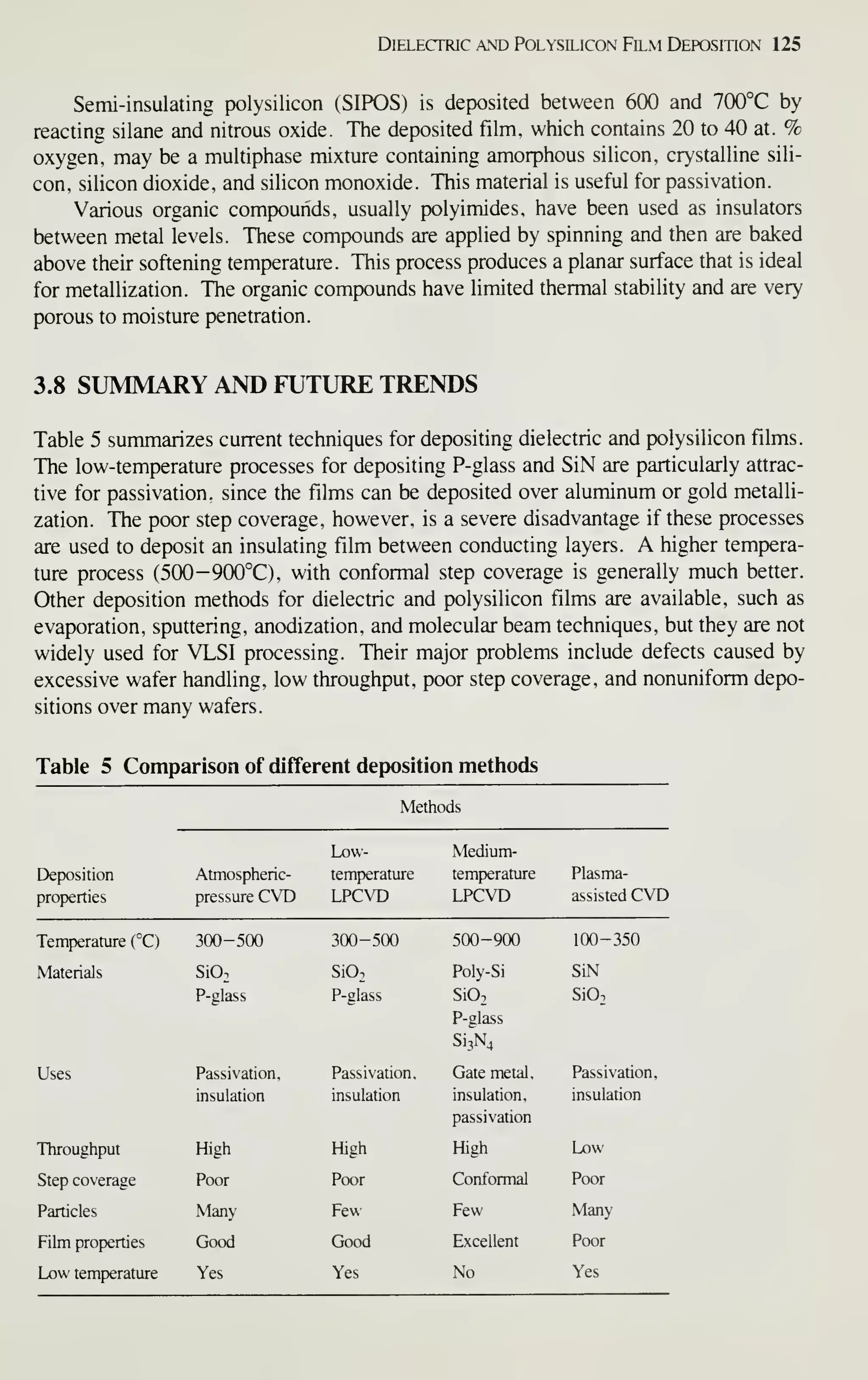
![Dielectric and Polysilicon Film Deposition 127
12] C. H. J. Van Den Brekel and L. J. M. Bollen. "Low Pressure Deposition of Polycrystalline Silicon
from Silane." y. Cnst. Growth. 54. 310 (1981).
13] F. C. Eversteyn and B. H. Put. "'Influence of ASH3. PH3. and B^H^, on the Growth Rate and Resis-
tivity of Polycrystalline Silicon Films Deposited from a SiH;
—
Ht Mixture," J. Electrochem. Soc,
120.106(1973).
14] T. I. Kamins, M. M. Mandurah. and K. C. Saraswat, "Structure and Stability of Low Pressure Chem-
ically Vapor-Deposited Silicon Films," 7. Electrochem. Soc, 125. 927 ( 1978).
15] T. I. Kamins. "Structure and Properties of LPCVD Silicon Films." J. Electrochem. Soc, 127. 686
(1980).
16] Y. Wada and S. Nishimatsu. "Grain Growth Mechanism of Heavily Phosphorus-Implanted Polycrys-
talline Silicon," 7. f/mroc/Tew. Soc. 125. 1499(1978).
17] T. 1. Kamins. "Resistivity of LPCVD Polycrystalline-Silicon Films," J. Electrochem. Soc, 126, 833
(1979).
18] M. M. Mandurah, K. C. Saraswat, and T. 1. Kamins, "Phosphorus Doping of Low Pressure Chemi-
cally Vapor-Deposited Silicon Films," J. Electrochem. Soc, 126, 1019 (1979).
19] M. M. Mandurah, K. C. Saraswat, C. R. Helms, and T. I. Kamins, "Dopant Segregation in Polycrys-
talline Silicon," J. Appl. Phys.. 51 , 5755 ( 1980).
20] T. I. Kamins, J. Manoliu, and R. N. Tucker, "Diffusion of Impurities in Polycrystalline Silicon," J.
Appl. Phys.. 43.^3 (1912).
21] D. J. Coe, "The Lateral Diffusion of Boron in Polycrystalline Silicon and its Influence on the Fabrica-
tion of Sub-Micron MOSTS," Solid State Electron., 20, 985 (1977).
22] T. 1. Kamins, "Hall Mobility in Chemically Deposited Polycrystalline Silicon," J. Appl. Phys., 42,
4357(1971).
23] S. Horiuchi, "Electrical Characteristics of Boron Diffused Polycrystalline Silicon Layers," Solid State
Electron., 18,659(1975).
24] G. Yaron, "Characterization of Phosphorus Implanted Low Pressure Chemical Vapor Deposited
Polycrystalline Silicon," Solid State Electron., 22, 1017 (1979).
25] M. Kuisl and W. Langheinrich, "Preparation and Properties of Phosphorus-Doped Polycrystalline Sil-
icon Films," in J. M. Blocher, Jr., H. E. Hintermann, and L. H. Hall, Eds., Chemical Vapor
Deposition —Fifth International Conference, Electrochemical Society. Princeton, N.J., 1975, pp.
380-389.
26] T. I. Kamins. "Oxidation of Phosphorus-Doped Low Pressure and Atmospheric Pressure CVD
Polycrystalline-Silicon Films." J. Electrochem. Soc, 126. 838 ( 1979).
27] B. G. Bagley, D. E. Aspnes, A. C. Adams, and C. J. Mogab, "Optical Prop)erties of Low-Pressure
Chemically Vapor Deposited Silicon Over the Energy Range 3.0-6.0 eV," Appl. Phys. Lett., 38, 56
(1981).
28] Ch. Kuhl, H. Schlotterer, and F. Schwidefsky, "Optical Investigation of Different Silicon Films," J.
Electrochem. Soc. 121, 1496(1974).
29] M. Hirose, M. Taniguchi, and Y. Osaka, "Electronic Properties of Chemically Deposited Polycrystal-
line Silicon," 7. Appl. Phys., 50, 377 (1979).
30] W. Kern and R. S. Rosier, "Advances in Deposition Processes for Passivation Films," J. Vac Sci.
Technol., 14, 1082(1977).
31] R. E. Logar, M. T. Wauk, and R. S. Rosier, "Low Pressure Deposition of Phosphorus-Doped Silicon
Dioxide at 400°C in a Hot Wall Furnace," in L. F. Donaghey. P. Rai-Choudhury, and R. N. Tauber,
Eds., Chemical Vapor Deposition—Sixth International Conference, Electrochemical Society, Prince-
ton, N.J. , 1977, pp. 195-202.
32] H. Huppertz and W. L. Engl, "Modeling of Low-Pressure Deposition of SIOt by Decomposition of
TEOS," IEEE Trans. Electron Devices, ED-26, 658 ( 1979).
33] A. C. Adams and C. D. Capio, "The Deposition of Silicon Dioxide Films at Reduced Pressure," J.
Electrochem. Soc, 126, 1042(1979).
34] K. Watanabe, T. Tanigaki, and S. Wakayama, "The Properties of LPCVD SiOj Film Deposited by
SiH^Cl, and N^O Mixtures," J. Electrochem. Soc, 128, 2630 (1981).
35] M. Maeda and H. Nakamura, "Deposition Kinetics of Si02 Film," J. Appl. Phys., 52, 6651 (1981).](https://image.slidesharecdn.com/simonm-220913174129-44ec6f82/75/Simon-M-Sze-editor-Very-Large-Scale-Integration-VLSI-Technology-McGraw-Hill-Inc-US-1983-pdf-147-2048.jpg)
![128 VLSI Technology
[36] M. Shibata, T. Yashimi, and K. Sugawara, "Deposition Rate and Phosphorus Concentration of Phos-
phosilicate Glass Films in Relation to PH3/SiH4+PH3 Mole Fraction." J. Electrochem. Soc, 122,
157(1975).
[37] P. J. Tobin, J. B. Price, and L. M. Campbell, "Gas Phase Composition in the Low Pressure Chemical
Vapor Deposition of Silicon Dioxide." J. Electrochem. Soc. 127. 2222 (1980).
[38] A. C. Adams and C. D. Capio. "Planarization of Phosphorus-Doped Silicon Dioxide," J. Electro-
chem. Soc, 128,423(1981).
[39] W. A. Pliskin, "Comparison of Properties of Dielectric Films Deposited by Various Methods." J.
Vac. Sci. Techiol., 14, 1064 (1977).
[40] A. C. Adams and S. P. Murarka, "Measuring the Phosphorus Concentration in Deposited Phosphosili-
cate Fihns," J. Electrochem. Soc, 126, 334 (1979).
[41] K. Chow and L. G. Garrison, "Phosphorus Concentration of Chemical Vapor Deposited Phosphosili-
cate Glass," J. Electrochem. Soc, 124, 1133 (1977).
[42] A. C. Adams, D. P. Schinke, and C. D. Capio, "An Evaluation of the Prism Coupler for Measuring
the Thickness and the Refractive Index of Dielectric Films on Silicon Substrates," J. Electrochem.
Soc, 126, 1539(1979).
[43] N. Nagasima, "Structure Analysis of Silicon Dioxide Films Formed by Oxidation of Silane," J. Appl.
P/m.. 43, 3378(1972).
[44] J. A. Appels, E. Kooi, M. M. Paffen, J. J. H. Schatorje, and W. H. C. G. Verkuylen, "Local Oxida-
tion of Silicon and its Application in Semiconductor Device Technology," Philips Res. Rep.. 25, 118
(1970).
[45] P. S. Peercy, H. J. Stein, B. L. Doyle, and S. T. Picraux, "Hydrogen Concentration Profiles and
Chemical Bonding in Silicon Nitride," J. Electron. Mat.. 8, 1 1 (1979).
[46] J. V. Dalton and J. Drobek. "Structure and Sodium Migration in Silicon Nitride Films," J. Electro-
chem. Soc 115,865(1968).
[47] J. R. Hollahan and R. S. Rosier, "Plasma Deposition of Inorganic Thin Films," in J. L. Vossen and
W. Kern, Eds., Thin Film Processes. Academic, New York, 1978, pp. 335-360.
[48] M. J. Rand, "Plasma-Promoted Deposition of Thin Inorganic Films," J. Vac Sci. Technol.. 16, 420
(1979).
[49] H. Dun, P. Pan, F. R. White, and R. W. Douse, "Mechanisms of Plasma-Enhanced Silicon Nitride
Deposition Using SiH4/N2 Mixture," J. Electrochem. Soc, 128, 1555 (1981).
[50] A. C. Adams, F. B. Alexander, C. D. Capio, andT. E. Smith, "Characterization of Plasma-Deposited
Silicon Dioxide," J. Electrochem. Soc, 128, 1545 (1981).
[51] W. A. Lanford and M. J. Rand, "The Hydrogen Content of Plasma-Deposited Silicon Nitride," J.
Appl. Phys.. 49. 2414 (I9m.
[52] A. K. Sinha and T. E. Smith, "Electrical Prof)erties of Si-N Films Deposited on Silicon from Reactive
Plasma," J. Appl. Phys., 49, 2756 (1978).
[53] M. J. Rand and J. F. Roberts, "Silicon Oxynitride Films from the NO—NH3 —SiHj Reaction," J.
Electrochem . 5oc. , 1 20, 446 ( 1 973)
.
[54] A. K. Gaind and E. W. Heam, "Physiochemical Properties of Chemical Vapor-Deposited Silicon
Oxynitride from a SiH4—C02—NH3—H2 System," y. Electrochem. Soc, 125. 139(1978).
PROBLEMS
1 Find the empirical formula for plasma silicon nitride containing 25 at. % H and having a Si/N ratio of 1 . 1
.
Find the empirical formula for LPCVD silicon nitride containing 5 at. % H and having a Si/N ratio of 0.75.
2 If plasma-deposited Si02 contains 3 x 10^' H/cm^, find the at. % H and the empirical formula.
3 If the average chlorine concentration within the first 1000 A of a deposited Si02 is 1 x lO'^ Cl/cm^, what
is the at. % CI in this region?
4 Derive the relationship between wt. % B, at. % B, and mol % B2O3 for boron-doped Si02.
5 A polysilicon deposition uses 30 % silane in nitrogen at 625°C and 53.3 Pa (0.4 Torr). The total gas flow
is 500 std. cm^/min. The volume of the LPCVD reactor is 20 L, its length is 150 cm, and a cross-sectional](https://image.slidesharecdn.com/simonm-220913174129-44ec6f82/75/Simon-M-Sze-editor-Very-Large-Scale-Integration-VLSI-Technology-McGraw-Hill-Inc-US-1983-pdf-148-2048.jpg)


![134 VLSI Technology
and
C* = Hpc (5)
where Co is the equiUbrium concentration in the oxide at the outer surface, C* is the
equihbrium bulk concentration in the oxide, p^ is the partial pressure in the gas adja-
cent to the oxide surface, pc is the partial pressure in the bulk of the gas, and H is
Henry's law constant. Using Henry's law along with the ideal gas law ^ allows us to
rewrite Cq and Cc
Cg = -r^ (6a)
kT
Ps_
kT
Ps
Cs = ^ (6b)
Combining Eqs. 3 to 6 gives
F, - h{C* - Co) (7)
where h is the gas-phase mass-transfer coefficient in terms of concentration in the
solid, given by h = Hq / HkT. When the concentration of the oxidant in the oxide at
the oxide-gas interface Co is less than the equilibrium bulk oxide concentration, F is
positive. Oxidation is a nonequilibrium process with the driving force being the devi-
ation of concentration from equilibrium.^ Henry's law is valid only in the absence of
dissociation effects at the gas-oxide interface. This implication is that the species
moving through the oxide is molecular.
The flux of this oxidizing species across the oxide is taken to follow Pick's law
^2= -D ^ (8)
da
at any point d in the oxide layer. D is the diffusion coefficient and dC / dd is the con-
centration gradient of the oxidizing species in the oxide. Following the steady-state
assumption, F2 must be the same at any point within the oxide (i.e., dFj/dd =0)
resulting in
^(Co - Q)
F2 = -^-^, (9)
do
where C, is the oxidizing species concentration in the oxide adjacent to the oxide-
silicon interface and do is the oxide thickness.
Assuming that the flux corresponding to the Si-Si02 interface reaction is propor-
tional to C,
F3 = k,Ci (10)
where k^ is the rate constant of chemical surface reaction for silicon oxidation.
After setting F] = Fj = Ft,, as dictated by steady-state conditions, and solving
simultaneous equations, we obtain the following expressions for C, and Co:](https://image.slidesharecdn.com/simonm-220913174129-44ec6f82/75/Simon-M-Sze-editor-Very-Large-Scale-Integration-VLSI-Technology-McGraw-Hill-Inc-US-1983-pdf-154-2048.jpg)
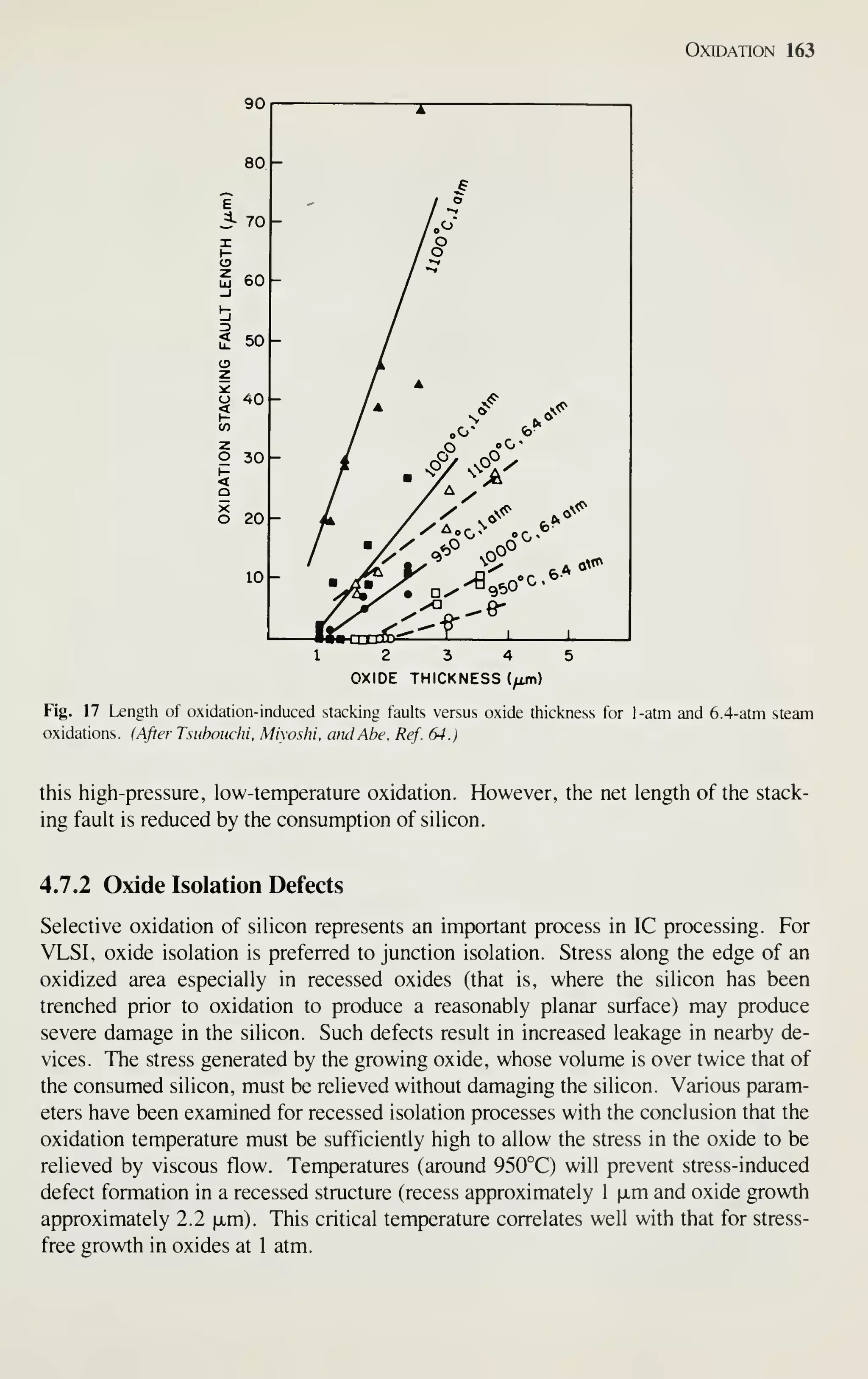
![162 VLSI Technology
TEMPERATURE (°C)
1200 1150 1100
"T
0.64 0.66 0.68 0.70
lO'/T (K-l)
0.72 0.74
Fig. 16 Growth of oxidation-induced stacking faults versus temperature; for 3 h of dry oxidation. (After
Hu.Ref.62.)
responsible for stacking fault growth. Equation 23 is a proposed model^' in which the
oxidation rate is the controlling parameter in oxidation stacking fault length.
dt
K,
dT,
dt
K, (23)
where / is the stacking fault length, Tq^ is the oxide thickness, t is the time, n is the
power dependence, .^i is related to the growth mechanism and defect generation at
the Si-Si02 interface, and K2 is related to the retrogrowth mechanism. Applying this
equation to experimental data gives values for n, K], and Kj- A 0.4th power depen-
dence is observed. ^^ This less-than-linear dependence of oxidation stacking fault
growth rate on the oxidation rate means that smaller stacking faults will result for a
higher oxidation rate at the same temperature for the same oxide thickness. This, of
course, is the case with high-pressure oxidation where the oxidation rate is increased.
Figure 17 shows an experimental result for a 950 to 1 100°C temperature range at both
1- and 6.4-atm pressure.^ The above results confirm the proposed model. Additional
results^^ at 700°C and 20-atm pressure show complete stacking fault suppression for
all thicknesses studies (up to 5 [xm). Preexisting stacking faults tend to grow during](https://image.slidesharecdn.com/simonm-220913174129-44ec6f82/75/Simon-M-Sze-editor-Very-Large-Scale-Integration-VLSI-Technology-McGraw-Hill-Inc-US-1983-pdf-182-2048.jpg)
![Oxidation 165
REFERENCES
[1] M. M. Alalia. "Semiconductor Surfaces and Films; the Si-SiOi System."' Properties of Elemental and
Co/npound Semiconductors. H. Gatos, Ed.. Interscience. New York. 1960. Vol. 5. pp. 163 — 181.
P. J. Jorgensen. "Effect of an Electric Field on Silicon Oxidation." J. Chem Phys.. 37, 874 (1962).
J. R. Ligenza and W. G. Spitzer. "The Mechanisms for Silicon Oxidation in Steam and Oxygen." J.
Phys. Chem. Solids. 14. 131 (1960).
B. E. Deal and A. S. Grove. "General Relationship for the Thermal Oxidation of Silicon." J. Appl.
Phys.. ^6. 3170 (1965).
A. S. Grove. Physics cmd Technology of Semiconductor Devices. Wiley. New York. 1967, Chapter 2.
E. H. .NicoUian and J. R. Breuws. MOS Physics and Technology. Wiley. New York. 1982.
U. R. Evans. "The Relationship Between Tarnishing and Corrosion." Trans. Electrochem. Soc, 46.
247(1924).
P. S. Flint. "The Rates of Oxidation of Silicon." Abstract 94. The Electrochem. Soc. Extettded Abs..
Spring Meeting. Los Angeles. .May 6- 10. 1962.
R. H. Doremus. "Oxidation of Silicon by Water and Oxygen and Diffusion in Fused Silica." J. Pins.
Chem.. m.113 (1916).
J. Blanc, "A Revised Model for the Oxidation of Si by Oxygen." Appl. Phys. Lett.. 33. 424 ( 1978).
T. G. Mills and F. A. Kroger. "Electrical Conduction at Eleated Temp, in Thermally Grown SiO-.
Films." J. Electrochetn. Soc. 120. 1582(1973).
W. A. Tiller. "On the Kinetics of the Thermal Oxidation of Silicon. I. A Theoretical Perspective." J.
Electrochem. Soc. 127. 619 (1980).
W. A. Tiller, "On the Kinetics of the Thermal Oxidation of Silicon. II. Some Theoretical Evalua-
tions," J. Electrochem. Soc, 127, 625 ( 1980).
W. A. Tiller. "On the Kinetics of the Thermal Oxidation of Silicon. III. Coupling With Other Key
Phenomena." J. Electrochem. Soc. 128. 689 ( 1981 ).
R. B. Fair, "Oxidation. Impurity Diffusion, and Defect Growth in Silicon—An Overiev. ." J. Elec-
trochem. Soc. 128. 1361 (1981).
S. M. Hu. "Formation of Stacking Faults and Enhanced Diffusion in the Oxidation of Silicon." J.
Appl. Pins.. 45. 1561 {1914).
F. N. Schuettmann. K. L. Chiang, and W. A. Brown, "Variation of Silicon Dioxide Growth Rate
with Pre-Oxidation Clean," Abstract 276, The Electrochem. Soc. Extended Abs.. Spring Meeting,
Seattle, Washington, May 1978.
E. A. Irene, "Silicon Oxidation Studies: Some Aspects of the Initial Oxidation Regime,"" J. Electro-
chem. Soc, 125, 1708(1978).
E. A. Taft, "The Optical Constants of Silicon and Dr} Oxygen Oxides,"" J. Electrochem. Soc. 125.
968(1978).
C. Hashimoto. S. .Muramoto. N. Shiomo. and O. Nakajima. "A Method of Forming Thin and Highly
Reliable Gate Oxides. ""y.£/mTOf/!£'w.5of.. 127. 129(1980).
A. C. Adams. T. E. Smith, and C. C. Chang. "The Growth and Characterization of Very Thin Silicon
Dioxide Films."" 7. Electrochem. Soc. 127. 1787 ( 1980).
M. Hirayama. H. .Miyoshi. N. Tsubouchi. and H. Abe. "High Pressure Oxidation for Thin Gate Insu-
lator Process."" IEEE Trans. Electron Devices. ED-29. 503 (1982).
J. R. Ligenza. "Effect of Cr>'stal Orientation on Oxidation Rates in High Pressure Steam."" Phys.
Chem.. 65.2011 i96).
W. A. Pliskin. "Separation of the Linear and Parabolic Terms in the Steam Oxidation of Si."" IBM J.
Res.Dev.. 10. 198(1966).
B. E. Deal, "Thermal Oxidation Kinetics of Silicon in PTogenic HiO and 5% HCI/H^O Mixtures,"
J. Electrochem. Soc. 125. 576 ( 1978).
E. A. Irene, "The Effects of Trace Amounts of Water of the Thermal Oxidation of Si in Oxygen,"" J.
Electrochem. Soc, 121, 1613 (1974).
M. M. Atalla and E. Tannenbaum. "Impurity Redistribution and Junction Formation in Silicon by
Thermal Oxidation."" BellSxst. Tech. J.. 39. 933 (1960).](https://image.slidesharecdn.com/simonm-220913174129-44ec6f82/75/Simon-M-Sze-editor-Very-Large-Scale-Integration-VLSI-Technology-McGraw-Hill-Inc-US-1983-pdf-185-2048.jpg)
![Oxidation 167
[56] R. B. Fair and J. C. C. Tsai, "Theory and Direct Measurement of Boron Segregation in SiO-i during
Dry. Near Dry and Wet O2 Oxidation." J. Electrochem. Soc. 125. 2050 (1978).
[57] S. P. Murarka. "Diffusion and Segregation of Ion-Implanted Boron in Silicon in Dr>' Oxygen
Ambients." Phys. Rev. B. 12. 2502 ( 1975).
[58] T. I. Kamins. "Oxidation of Phosphorous-Doped Low Pressure and Atmospheric Pressure CVD
PolycrN'Stalline-Silicon Films." J. Electrochem. Soc. 126. 838 ( 1979).
[59] H. Sunami, "Thermal Oxidation of Phosphorus-Doped Polycrvstalline Silicon in Wet Oxygen." J.
Electrochem. Soc. 125. 892 (1978).
[60] E. A. Irene, E. Tiemey, and D. W. Dong. "Silicon Oxidation Studies: Morphological Aspects of the
Oxidation of Polycrystalline Silicon." J. Electrochem. Soc, 127, 705 (1980).
[61] A. Lin, R. W. Dutton, D. A. Antoniades, and W. A. Tiller. "The Growth of Oxidation Stacking
Faults and the Point Defect Generation at Si-SiOi Interface during Thermal Oxidation of Silicon." J.
Electrochem. Soc. 128. 1121 (1981).
[62] S. M. Hu. "Anomalous Temperature Effect of Oxidation Stacking Faults in Silicon." Appl. Phys.
Lett.. 1, 165 (1915).
[63] H. Shiraki. "Stacking Fault Generation. Suppression and Grown-In Defect Elimination in Dislocation
Free Silicon Wafers by HCl Oxidation." Jpn. J. Appl. Phys.. 15. 1 ( 1976).
[64] N. Tsubouchi. H. Miyoshi. and H. Abe. "Suppression of Oxidation-Induced Stacking Fault Forma-
tion in Silicon by High Pressure Steam Oxidation." J. Appl. Phys., 17, 223 (1978).
[65] L. E. Katz and L. C. Kimerling. "Defect Formation During High Pressure. Low Temperature Steam
Oxidation of Silicon." J. Electrochem. Soc, 125. 1680 ( 1978).
[66] D. Kahng. T. A. Shankoff. T. T. Sheng. and S. E. Haszko. "A Method for Area Saving Planar Isola-
tion O.xides Using Oxidation Protected Sidewalls." J. Electrochem. Soc, 127. 2468 (1980).
4.9 PROBLEMS
1 Show from the densities and molecular weights of Si and SIOt that a layer of silicon of thickness 0.45 dQ
is consumed when a SiOn layer of thickness cIq is formed. Use densitv' values of 2.27 gm/cm-^ for Si02 and
2.33 gm/cm- for Si.
2 Show that in Eq. 14. d^ + Ado = B(t + i) reduces to d^ = Bt for long times and to dQ = B I A {t + t)
for short times.
3 (a) Show that in Eq. 14. c/q + .4^0 ~ ^(' + "J"' can be used graphically to obtain an equation describing
the oxidation rate.
(b) Generate such a plot for the 1 100°C oxidation data of Fig. 5. Use t = and ( 100) orientation to
obtain rate constants. Compare your results to those of Fig. 3.
4 Using Eq. 14 and Table 1 . how long will it take to grow 2.0 fxm of SIOt at 920°C and 25-atm steam pres-
sure?
5 Define a set of conditions to minimize the chance of inverting the surface of an n-type substrate (contain-
ing a boron diffusion) when oxidizing the wafer.
6 List possible ways of growing an initial oxide on a substrate without forming oxidation-induced stacking
faults.
7 Solve Eq. 14 for oxide thickness as/ (r. t. A, B).
8 Make use of the equation derived in Problem 7. and the data in Tables 1 and 2, to generate oxide thick-
ness versus time curves for wet and dry oxidations at 1 100°C. Assume t = 0.
9 Generate a model showing possible interface reaction and point-defect fluxes at the interface.
10 Devise a processing scheme to generate selectively a planar recessed oxide in silicon. Show how you
might prevent lateral oxidation during the oxide growth.](https://image.slidesharecdn.com/simonm-220913174129-44ec6f82/75/Simon-M-Sze-editor-Very-Large-Scale-Integration-VLSI-Technology-McGraw-Hill-Inc-US-1983-pdf-187-2048.jpg)

![170 VLSI Technology
defects, vacancies and interstitial atoms, and impurity atoms. The continuum theory
describes the diffusion phenomenon from the solution of Pick's diffusion equation
with appropriate diffusivities. (This chapter uses the terms "diffusivity" and "diffu-
sion coefficient" interchangeably.) The diffusivities of a dopant element can be deter-
mined from experimental measurements, such as the surface concentration, junction
depth, or the concentration profiles, and the solutions of Pick's diffusion equation.
When impurity concentrations are low, the measured diffusion profiles are well
behaved and agree with Pick's diffusion equation with a constant diffusivity which
can be calculated readily. In these cases the detailed atomic movements do not have
to be known. When impurity concentrations are high, the diffusion profiles deviate
from the predictions of the simple diffusion theory, and the impurity diffusion is
affected by other factors, which are not considered in Pick's simple diffusion laws.
Since the diffusion profile measurements reveal concentration-dependent diffusion
effects, we apply Pick's diffusion equation with concentration-dependent diffusivities
to the high-concentration diffusions. The concentration-dependent diffusivities are
determined by a Boltzmann-Matano analysis'^ or other formulations of profile
analysis.
Various atomistic diffusion models based on defect-impurity interactions have
been proposed to explain the experimental results from concentration-dependent dif-
fusivities and other anomalous diffusions. The atomistic diffusion theory is still
undergoing active development. Theoretical and experimental results on the diffusion
of Group III and V elements in silicon have been incorporated into various process
models. Chapter 11 discusses the process models in detail. Because process model-
ing is still developing we have to be aware of the model's limitations.
5.2 MODELS OF DIFFUSION IN SOLIDS
At high temperatures point defects, such as vacancies and interstitial atoms, are gen-
erated in a single-crystal solid. When a concentration gradient of the host or impurity
atoms exists, the point defects affect atom movement (diffusion). Diffusion in a solid
can be visualized as atomic movement of the diffusant in the crystal lattice by vacan-
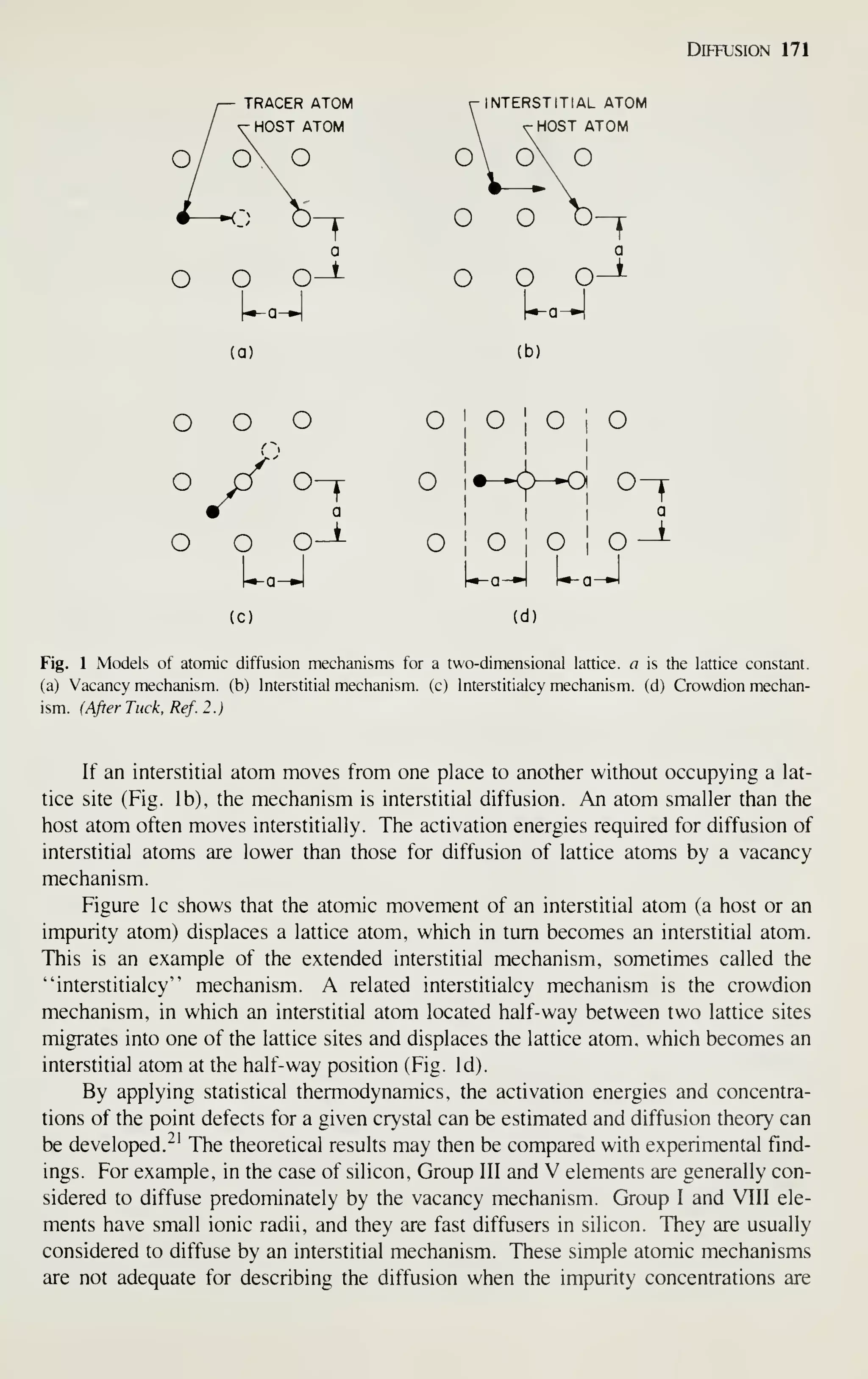
cies or self-interstitials. Pigure 1 shows some common atomic diffusion models" in a
solid, using a simplified two-dimensional crystal structure with lattice constant a.
The circles represent the host atoms occupying the low-temperature lattice positions.
The solid circles represent either host or impurity atoms. At elevated temperatures
the lattice atoms vibrate around the equilibrium lattice sites. Occasionally a host
atom acquires sufficient energy to leave the lattice site, becoming an interstitial atom
and creating a vacancy. When a neighboring atom (either the host or the impurity
atom) migrates to the vacancy site, the mechanism is called diffusion by a vacancy
(Pig. la). If the migrating atom is a host atom the diffusion is referred to as self-
diffusion; if it is an impurity atom the diffusion is impurity diffusion. [Self-diffusion
experiments are usually conducted by introducing radioactive isotopes of the host
atom (Pig. la).]](https://image.slidesharecdn.com/simonm-220913174129-44ec6f82/75/Simon-M-Sze-editor-Very-Large-Scale-Integration-VLSI-Technology-McGraw-Hill-Inc-US-1983-pdf-190-2048.jpg)
![Diffusion 175
Redistribution diffusion In bipolar linear ICs, redistribution diffusion from a
predeposition diffused layer is an important step. The redistribution diffusion in a
nonoxidizing ambient has been studied extensively. In VLSI technology, no inten-
tional rediffusion is applied in order to keep the diffusion depth shallow. From an ion
implanted source, however, some redistribution diffusion can occur while thermally
annealing the ion implanted region for electrical activation at temperatures greater
than 1000°C. The solution to Pick's equation, Eq. 4, with an initial ion implanted
Gaussian distribution has been obtained.^
The equation for redistribution diffusion in an oxidizing ambient involves a mov-
ing boundary problem and is more difficult to solve. No analytical solutions have
been found. A mathematical formulation of diffusion in an oxidizing ambient from a
given initial profile has been obtained;'' however, the solution involves expressions
that require numerical integration. Segregation of impurity atoms during oxidation
between the growing oxide and silicon was discussed in Chapter 4. Since redistribu-
tion diffusion is not important in VLSI technology, we will not discuss it in this
chapter.
5.3.2 Concentration-Dependent Diffusivities
At high concentrations, when the diffusion conditions are close to the constant surface
concentration case or to the constant total dopant case, the measured impurity profiles
deviate from Eqs. 8 and 12, respectively. In these high-concentration regions, the
impurity profile can often be represented by concentration-dependent diffusivities.
Equation 3 is used to determine the concentration-dependent diffusivities from the
experimentally measured concentration profiles. This section considers diffusion
under two conditions: constant surface concentration and a constant total dopant.
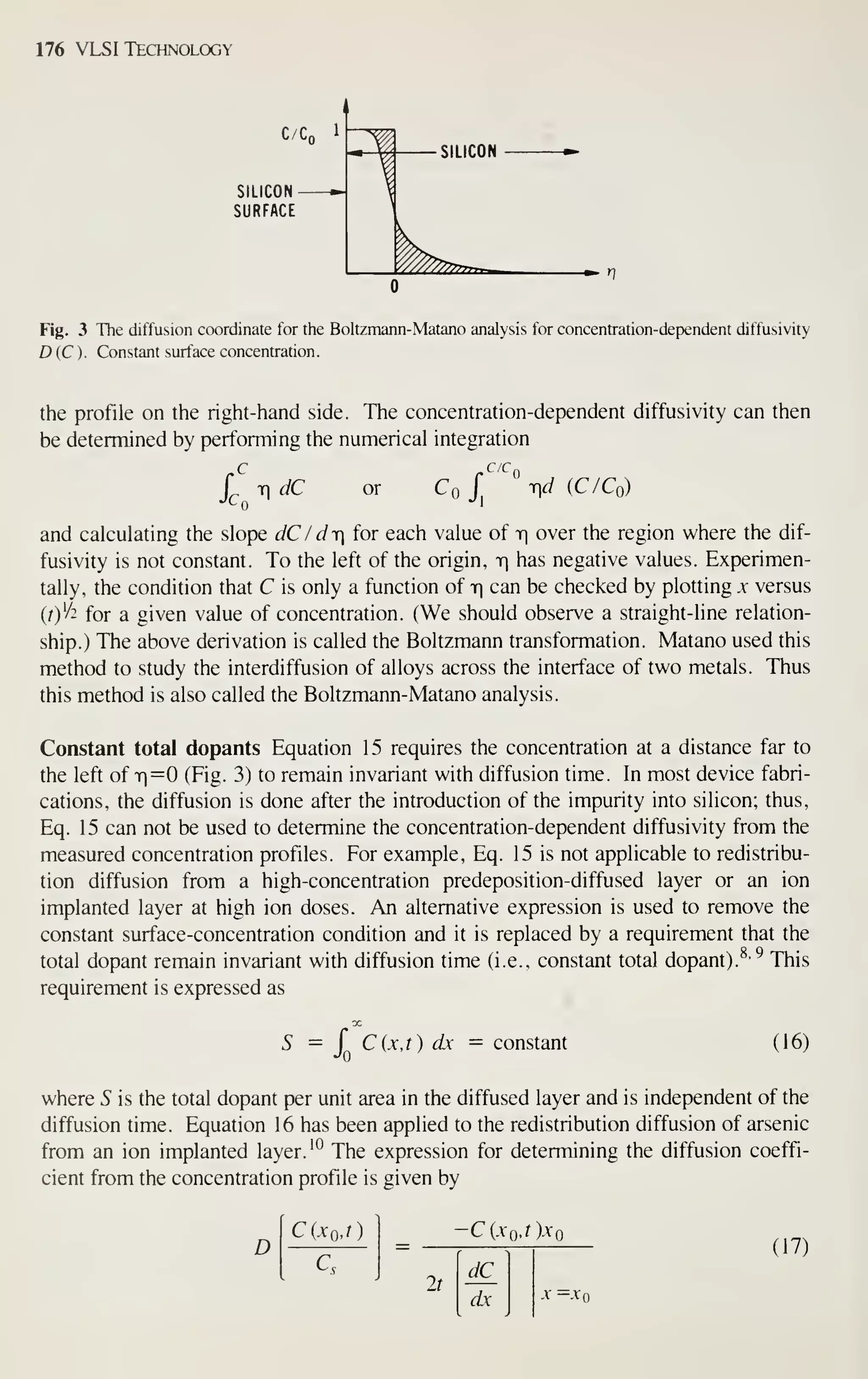
Constant surface concentration The one-dimensional diffusion equation with a
concentration-dependent diffusion coefficient was given in Eq. 3. If D is only a func-
tion of the concentration C and the surface concentration is maintained at a constant
value, Eq. 3 can be transformed into an ordinary differential equation"^ with a new
variable iq, where
m =
^ (14)
Thus, both D and C depend on x implicitly. After a change of variable to t], Eq. 15
can be obtained from Eq. 3:
-V2/^ T] dC
D(C) = -^ (15)
dT
Equation 15 refers to an infinite system. To determine the concentration-dependent
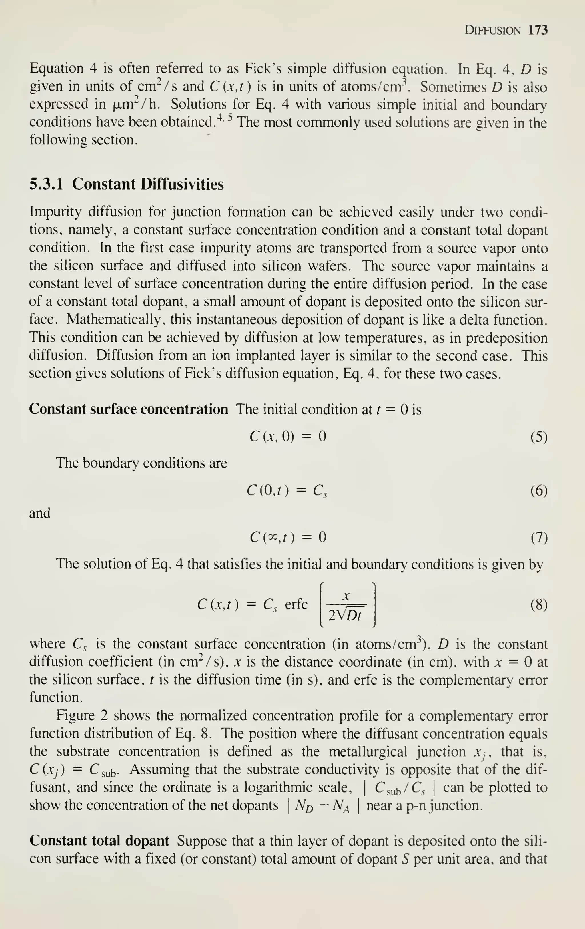
diffusivity from Eq. 15, we first plot the measured diffusion profile as concentration
(or normalized concentration) versus r (see Fig. 3). We choose the origin of the
abscissa so that the area under the profile on the left-hand side equals the area under](https://image.slidesharecdn.com/simonm-220913174129-44ec6f82/75/Simon-M-Sze-editor-Very-Large-Scale-Integration-VLSI-Technology-McGraw-Hill-Inc-US-1983-pdf-195-2048.jpg)
![Diffusion 179
where K^, is the equihbrium constant, a^ is the cheniical activity of element A, % is
the chemical activity of element B, qq is the chemical activity of the product C, and
a.h, and c represent the mole concentration of elements A, fi, and C of the reaction
shown in Eq. 21. For a dilute solution (a near ideal solution), the activities can be
replaced by the concentrations^ of the reactants and products according to Rault's law,
and Eq. 22 becomes
K^
CY
(23)
where [A] is the concentration of element A, {E is the concentration of element fi,
and [C] is the concentration of element C.
The law of mass action has been applied to dilute solid solutions where point
defects in a solid are considered as dilute solid solutions of defects in the crystal lat-
tice. The law of mass action is applicable to a dilute solid solution when the reactions
are in thermal equilibrium and sometimes applicable when the reactions are in quasi-
thermal equilibrium.
Vacancy and interstitial concentrations can be determined from statistical ther-
modynamics. They are expressed in terms of entropies of formation AS and forma-
tion energies A//. For a neutral monovacancy in silicon, the concentration Cy can be
expressed as
20
C^, =5.5 X 10-^ exp
'as^5
k
exp
kT
(24)
where XSy is the entropy of formation of a neutral monovacancy, A//v is the forma-
tion energy of a neutral monovacancy (expressed in eV). The superscript x represents
a neutral charge state of the defect. The subscript V denotes a vacancy defect.
For silicon. A/Zy is estimated to be greater than or equal to 2.5 eV and AS'v is
estimated to equal 1.1^. Thus the intrinsic concentration of monovacancy at the dif-
fusion temperatures of interest is rather low for silicon.
For an extrinsic silicon, the acceptor-type vacancy concentration can be
expressed as'^
1 + T^ exp
Cv" =
Ey - E,
kT
1 + ^/2 exp
Ev - Ef
QiV-)
Ey ~ Ej
kT
Ey - Ef
kT
kT
Q(V-)
(25)](https://image.slidesharecdn.com/simonm-220913174129-44ec6f82/75/Simon-M-Sze-editor-Very-Large-Scale-Integration-VLSI-Technology-McGraw-Hill-Inc-US-1983-pdf-199-2048.jpg)
![180 VLSI TECHN0LCX3Y
for (Ey — Ef)'»kT and {By — Ei)y>kT. Cy is the acceptor vacancy concentration
in the extrinsic siHcon, C, (V") is the acceptor vacancy concentration in the intrinsic
sihcon, Ey is the acceptor vacancy energy level (in eV), £, is the intrinsic Fermi level
(in eV), and Ef is the Fermi level of the extrinsic silicon (in eV). Thus,
C,
exp
C,{V-)
But for the nondegenerate case, we obtain
n = /I, exp
for n-type silicon, and Eq. 26 becomes
Cy-
Ei
kT
Ef - Ei
(26)
kT
(27)
If the impurity diffusion is dominated by the acceptor monovacancy mechanism, the
diffusion coefficient is approximately proportional to the acceptor monovacancy con-
centration. Thus, we have
-^ = ^ (28)
D, n,
where D is the diffusion coefficient in extrinsic silicon, and D, is the diffusion coeffi-
cient in intrinsic silicon.
The intrinsic carrier concentration /i, can be calculated using the following empir-
ical formula:
'*
where
n] = 1.5 X 10-^3 j2>
expt(-1.21 + ^Eg)/kT]
•/2
^Eo = -7.1 X 10"
T
(29)
(30)
and an assumed fg = 1.21 eV.
Equation 28 states that the interaction of the impurity atoms with charged accep-
tor vacancies leads to a dependence of the diffusion coefficient on the Fermi level at
the diffusion temperature. Since vacancies and interstitials can have various charge
states, Eq. 28 can be generalized to include all possible combinations of impurity-
point defect interactions.'^
D = D' + % iD-') + t (E>^')
n,
(31)
where D x for neutral defects, (D "''
), and (D ^^ ) refer to the intrinsic impurity dif-
fusivities associated with the particular charge states, r, of the point defects that affect
the impurity diffusion and r is an integer 1, 2, 3, . .
.
, m. For example, D^ represents
the intrinsic diffusivity of impurity interaction with a neutral-point defect; (D "), (r =](https://image.slidesharecdn.com/simonm-220913174129-44ec6f82/75/Simon-M-Sze-editor-Very-Large-Scale-Integration-VLSI-Technology-McGraw-Hill-Inc-US-1983-pdf-200-2048.jpg)
![Diffusion 185
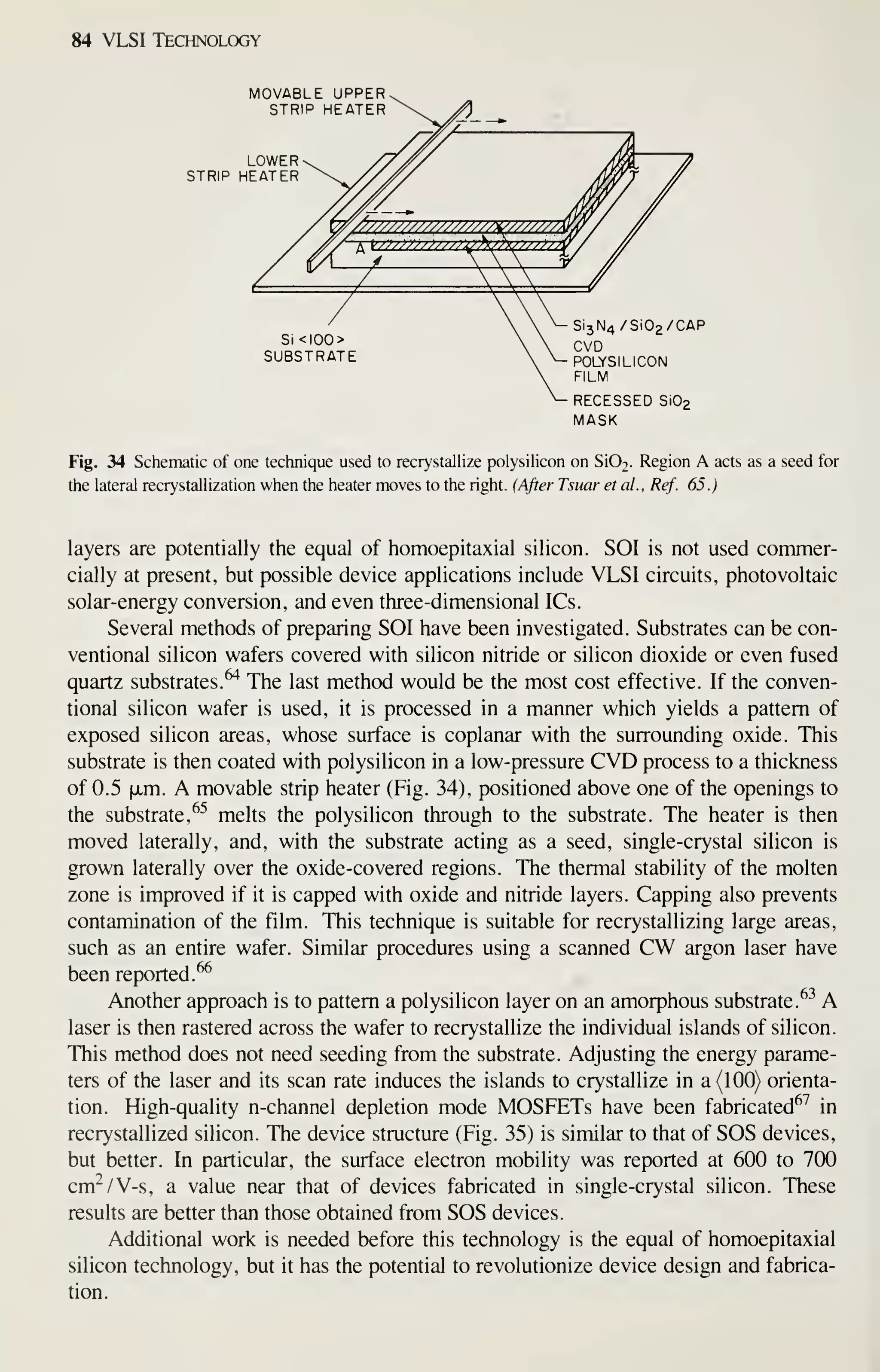
Table 1 Correction factor C.F. for the measurement
of sheet resistances with the four-point probe-^
Circle Square
Rectangle
d/s diam d/s a/d^ 1 a/d = 2 a/d = 3 a /d^4
1.0 0.9988 0.9994
1.25 1.2467 1.2248
1.5 1.4788 1.4893 1.4893
1.75 1.7196 1.7238 1.7238
2.0 1.9475 1 .9475 1 .9475
2.5 2.3532 2.3541 2.3541
3.0 2.2662 2.4575 2.7000 2.7005 2.7005
4.0 2.9289 3.1137 3.2246 3.2248 3.2248
5.0 3.3625 3.5098 3.5749 3.5750 3.5750
7.5 3.9273 4.0095 4.0361 4.0362 4.0362
10.0 4.1716 4.2209 4.2357 4.2357 4.2357
15.0 4.3646 4.3882 4.3947 4.3947 4.3947
20.0 4.4364 4.4516 4.4553 4.4553 4.4553
40.0 4.5076 4.5120 4.5129 4.5129 4.5129
oc 4.5324 4.5324 4.5325 4.5325 4.5324
measuring the voltages for current flowing in two directions, and then averaging the
two readings. This average reading removes some of the effect of contact resistance.
If the voltage differences are large, however, probe points and the cleanliness of the
sample surface should be checked. To ensure that the readings are correct, the sheet
resistances at two or three current levels can be measured. These measurements show
whether the measured sheet resistances are constant over the range of measured
currents. For high-resistivity silicon, annealing the sample in N2 at 150°C for a few
minutes improves the accuracy of readings. Always try to use as low current as possi-
ble to avoid ohmic heating or to avoid reaching the punchthrough voltage.
For a diffused layer, an average sheet resistance R^ is related to the junction
depth Xj , the carrier mobility ji, and the impurity distribution C (x ) by the following
expression:
Rs =
-r-^ (38)
^ X' M-CU) dx
The depletion of charge carriers near Xj can be neglected in the above calculation. In
general, the mobility is a function of the total impurity concentration, and often an
effective mobility is defined as
P x[C{x)]C(x)dx
^Jleff - -—V (39)
fJC{x)dx](https://image.slidesharecdn.com/simonm-220913174129-44ec6f82/75/Simon-M-Sze-editor-Very-Large-Scale-Integration-VLSI-Technology-McGraw-Hill-Inc-US-1983-pdf-205-2048.jpg)
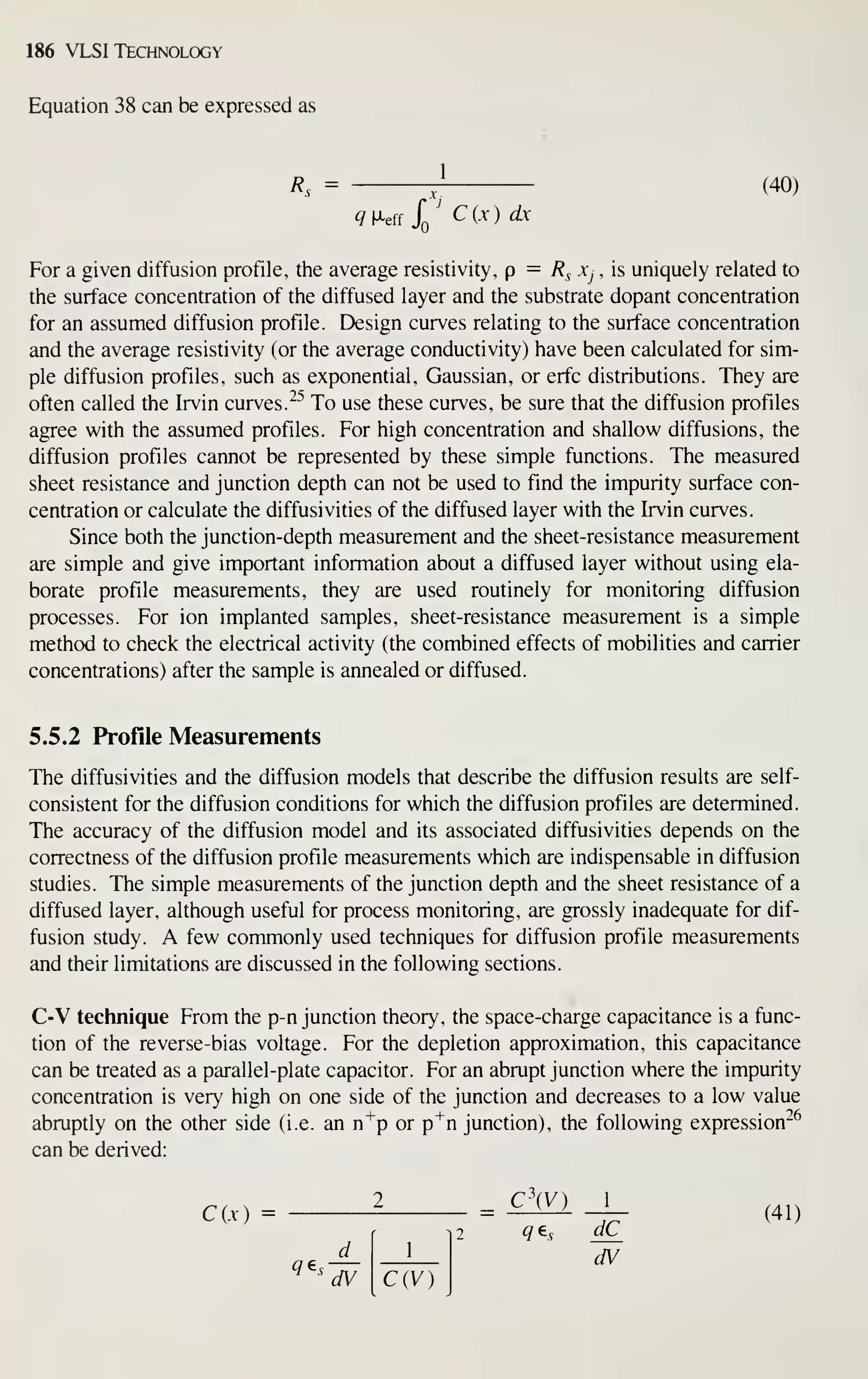
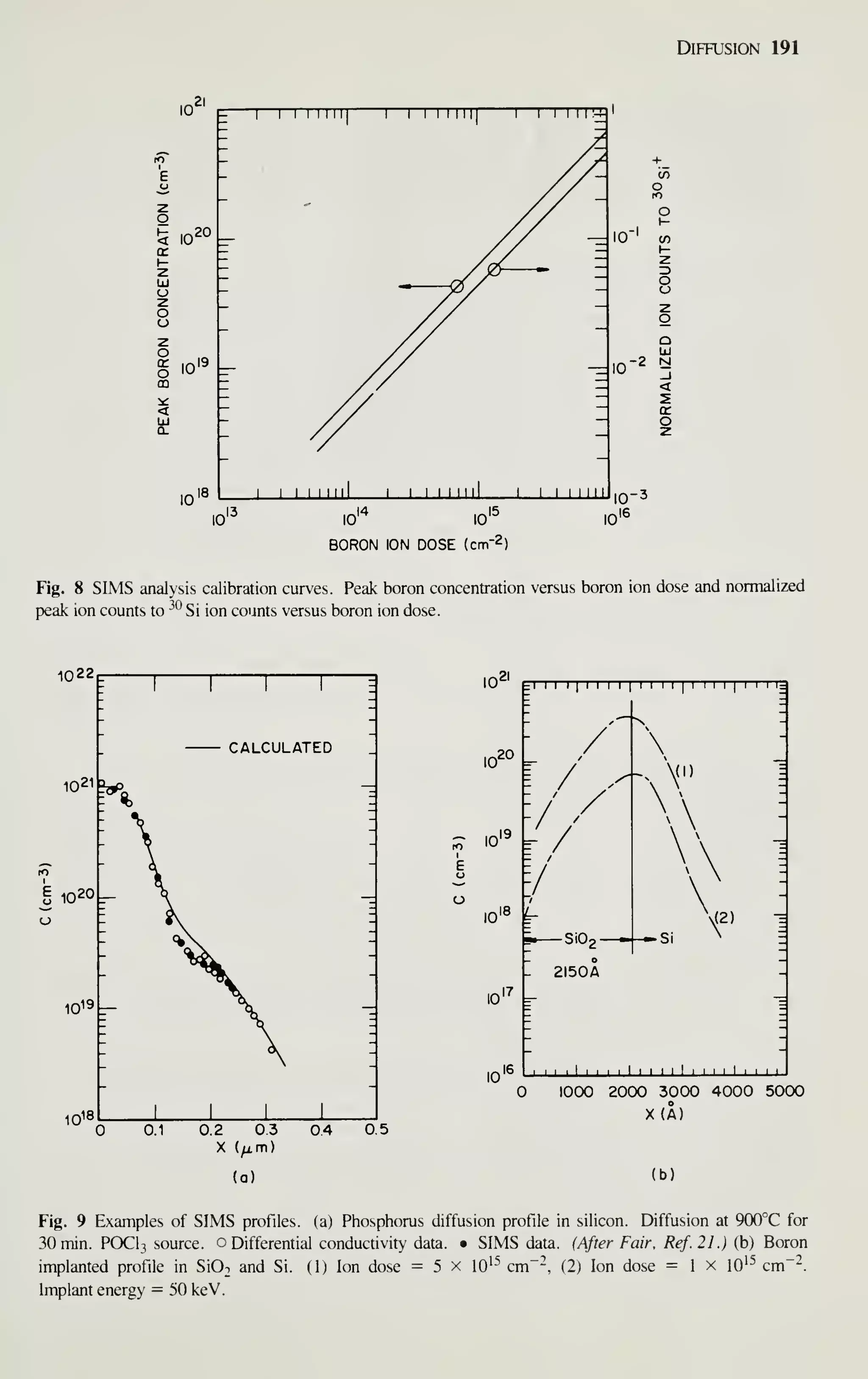
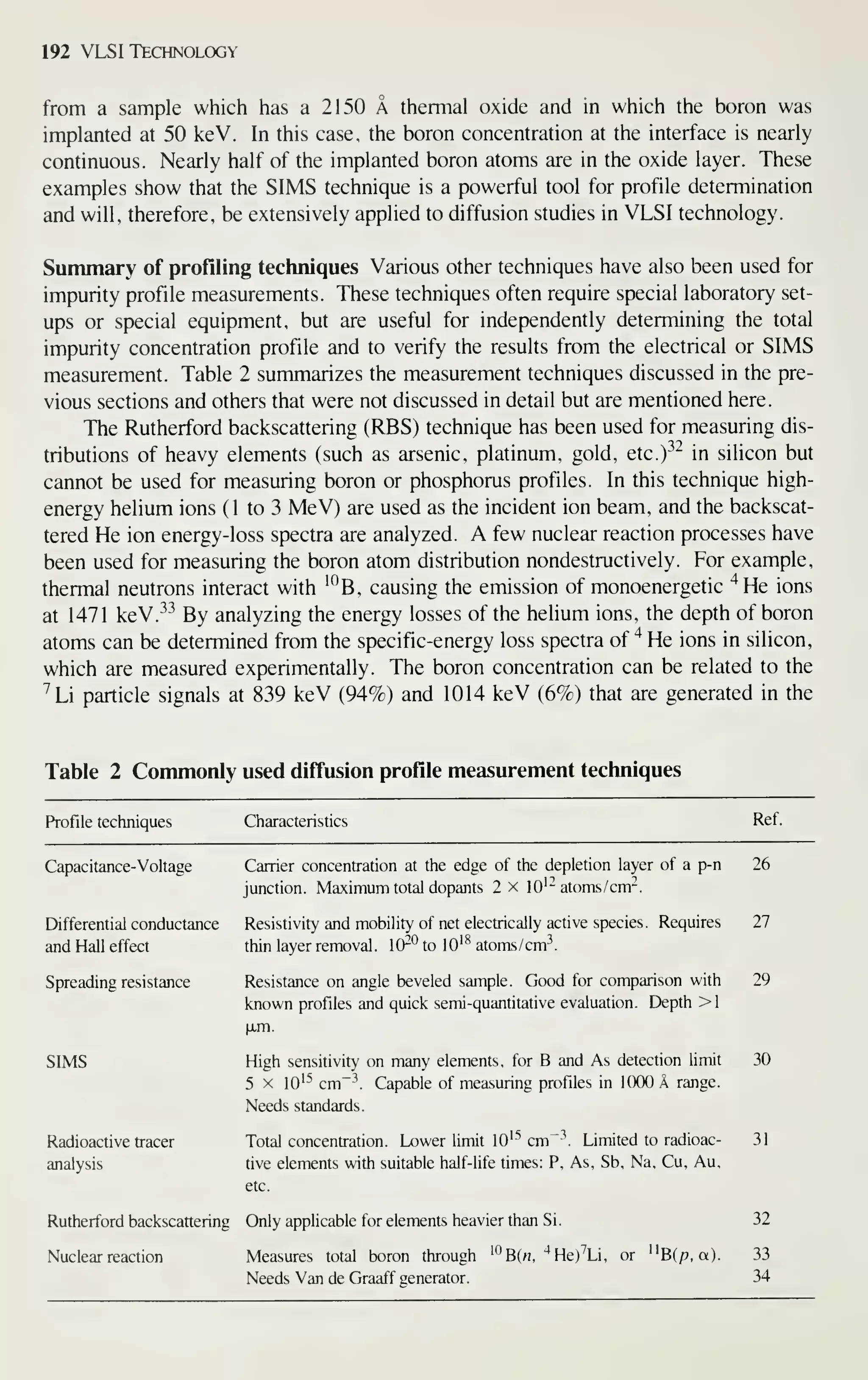
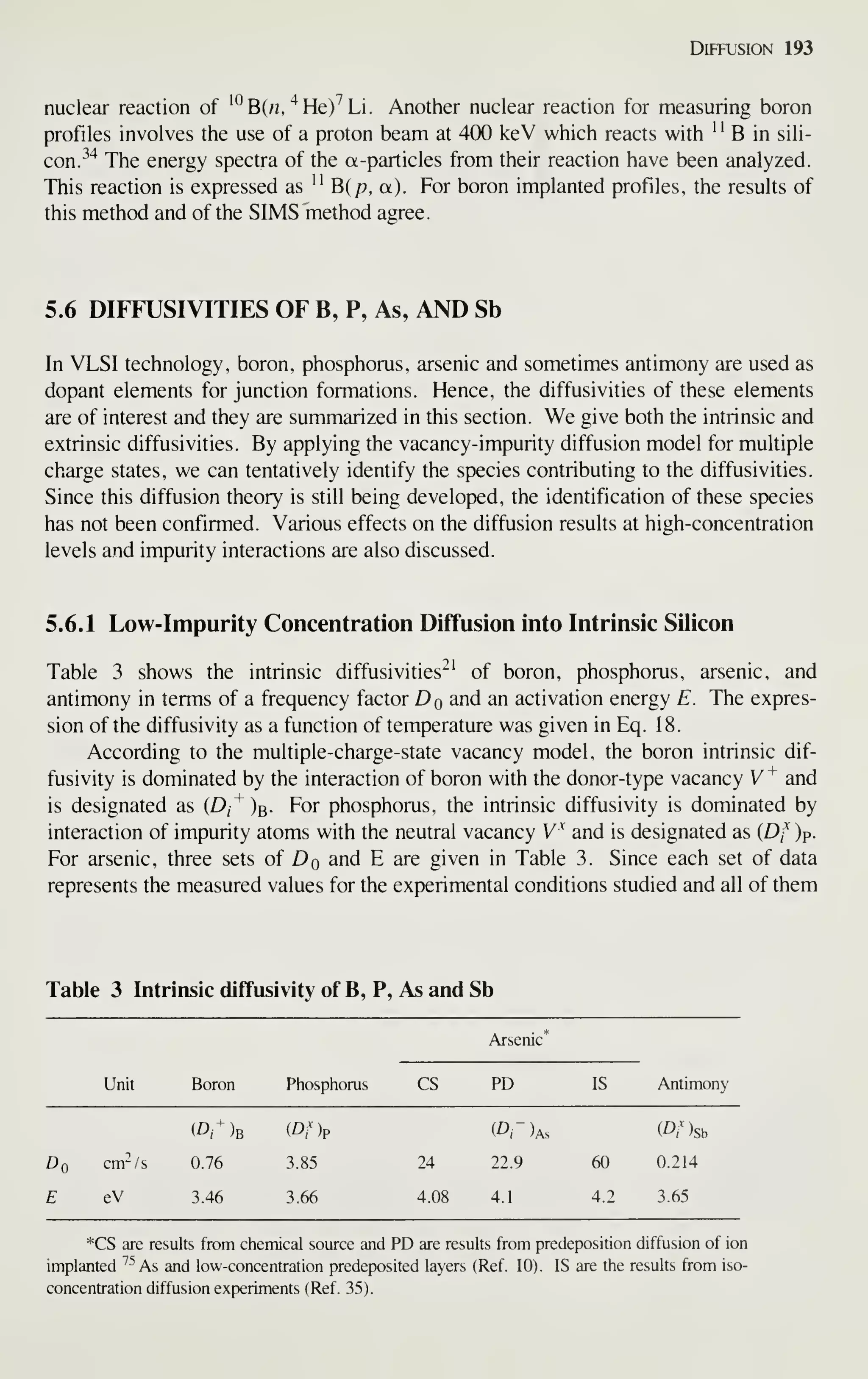
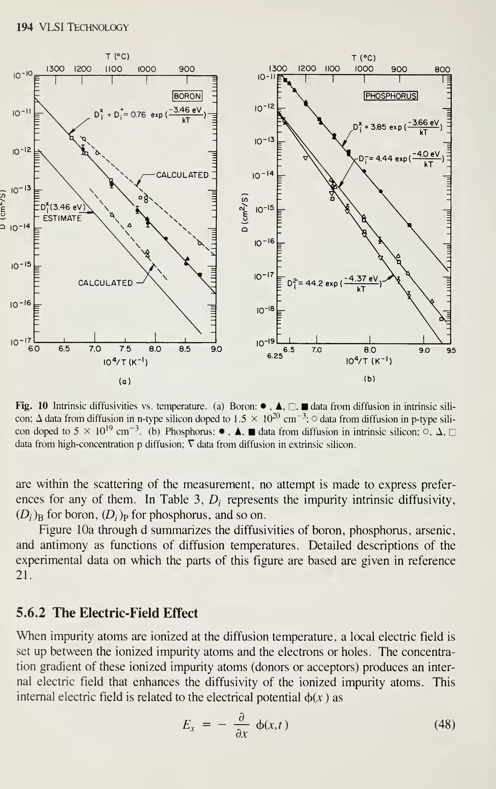
![T (°C)
1300 1200 1100 1000 900
M
^ 10-'"
J
E
10-15
IO-'8
- ] 1 1
AX V —D» *D-
. lARSENICl :
^V^ —
= -
= Vf ^ _
' N^ ^ _
V 'A
r %
-07(4.05 eV)-''^^
^D*(3.44 eV) -^
"^-^
—
~
*s >^ -
- N1^.
y^ -
— ^v^ ^
- y *. 3
- y^
_ CALCULATED -''
^
= (3.42 eV)
^
- i&^Nx I
— —
^
N
1 1
1
1
60 6.5 7,0 7.5 8.0 85 9.0
ioVt(k-I)
(c)
Diffusion 195
TCC)
1300 1200 1100 1000 900
6.0 65 7.0 7.5 8.0 85 90
lO^/T (K"')
(d)
Fig. 10 (continued) (c) Arsenic: • . . Z. c. A data from diffusion in intrinsic silicon; , V data from dif-
fusion in extrinsic silicon, (d) Antimony: o data from diffusion in intrinsic silicon; • data from diffusion in
extrinsic silicon. (After Fair, Ref. 21 .}
For a donor impurity, (t)(.v,r ) can be expressed as
(|)CT,r) = (Ec - EpMq (49)
where Ec is the conduction band energy and Ef is the Fermi level. Assuming that a
charge neutrality exists between the ionized donor and the electron and that all donor
atoms Njj are ionized, we have np = rij^ and N^ = «. It can be shown that
kT d ,
E^ = — — In
q dx
The diffusion flux in an electric field can be expressed as
d^D q
y = - qD—^ - qZD-^ No E,
dx kT
(50)
(51)
where Z is the charge state of the donor atoms. For a singly charged donor atom,
Z = 1. By substituting Eq. 50 into Eq. 51 and by changing variables from 6/6jc to
id I dNo )idNo / a.r ), Eq. 5 1 becomes
dNo](https://image.slidesharecdn.com/simonm-220913174129-44ec6f82/75/Simon-M-Sze-editor-Very-Large-Scale-Integration-VLSI-Technology-McGraw-Hill-Inc-US-1983-pdf-215-2048.jpg)
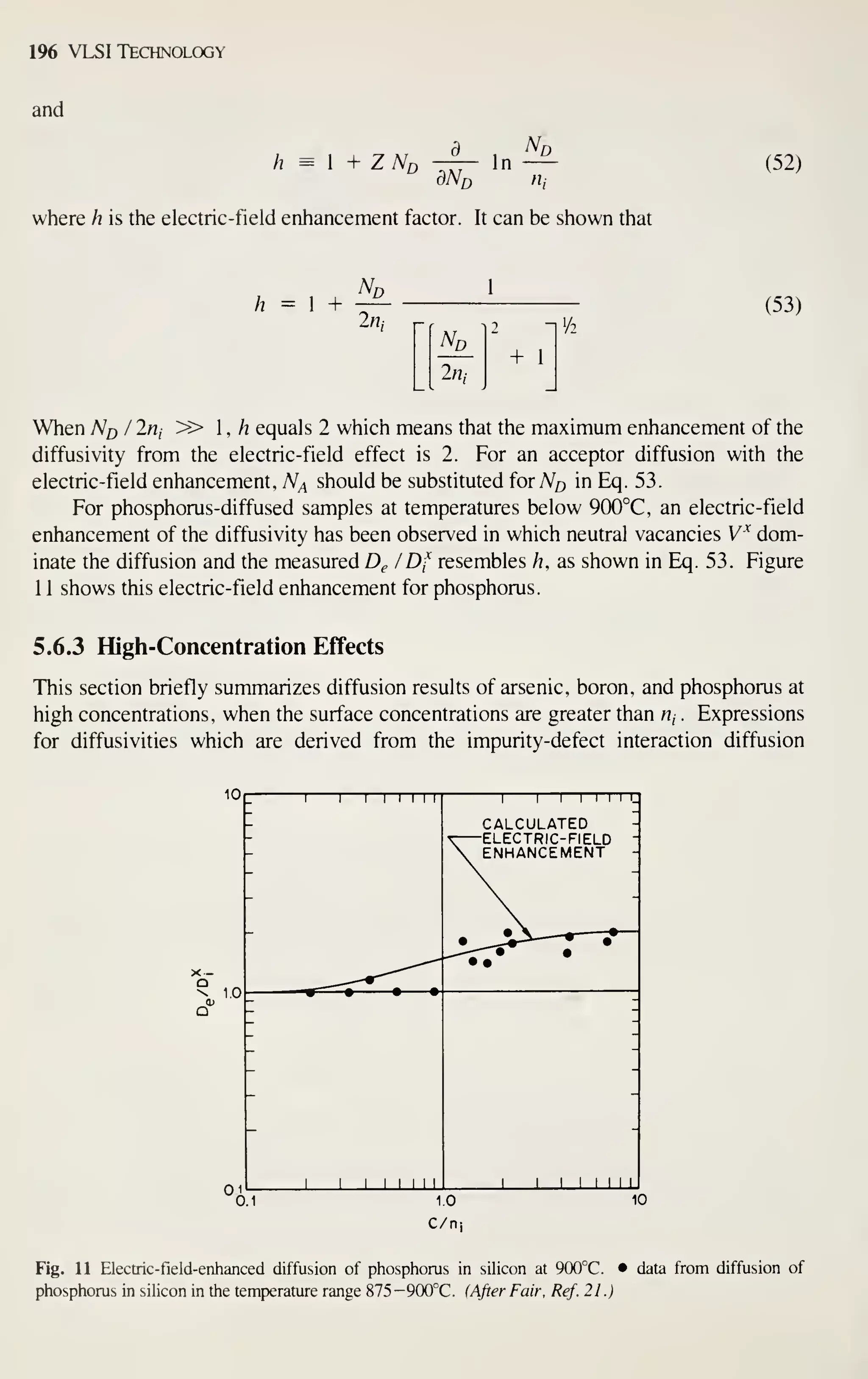
![Diffusion 197
model are given. For high-concentration arsenic, we discuss a model for the cluster
formation of impurity atoms. This model explains the observation that only a portion
of the diffused arsenic atoms is electrically active at room temperature. Similar
results are also observed for high-concentration boron-diffused layers. Results from a
phosphorus diffusion model are also given.
Arsenic According to the multi-charge-state, impurity-defect interaction model, the
arsenic diffusivity can be expressed as^^
Das = (2«/n,)(D,)As (54)
Equation 54 is similar to Eq. 28; the factor 2 represents the electric-field effect. A
similar expression based on interactions of charge vacancy with arsenic is-^^
1 + yn In;
Das = —TT (A)as (55)
1 + 7
with 7 = 100 for donor-impurity diffusions. Thus, D^s calculated from Eq. 54 is
almost twice that of D as calculated from Eq. 55.
The electric activity of arsenic from ion implanted samples depends on the ion
dose and the annealing or diffusion temperatures. For arsenic-ion doses below
1 X 10^^ cm~~ and diffusion temperatures greater than 1000°C, nearly all of the
arsenic atoms are ionized and contributing to the electrical activities. '° However, for
diffusion temperatures below 1000°C and an arsenic-ion dose greater than 10^^ cm"'^,
the concentration of ionized arsenic is a fraction of the total arsenic, and the differ-
ences become greater^^ as the diffusion temperature decreases below 900°C.
The difference between the ionized and the total arsenic can be explained by an
arsenic clustering model. In this model, arsenic atoms form clusters that are partially
active when their concentration is above 10^^ cm~^. The most recent clustering
model consists of three arsenic atoms and one electron that are electrically active at
the diffusion (or annealing) temperature and electrically neutral at room tempera-
ture.^'' The model is expressed as
high temp. 25°C
3As+ + e- ^_^ AS3+2 _^ As3 (56)
Applying the law of mass action to the high-temperature region, the equilibrium con-
stant is
[AS3+2]
K^ = :, (57)
and the carrier concentration at the annealing/diffusion temjDerature is
n = [As^] + 2[As3+2-] (58)
where [As"*"] is the carrier concentration from isolated arsenic atoms and 2[As3"^^] is
the carrier concentration as the arsenic clusters [As3^^] at high temperatures. At room
temperature, [As3^^] is electrically neutral and the carrier concentration is](https://image.slidesharecdn.com/simonm-220913174129-44ec6f82/75/Simon-M-Sze-editor-Very-Large-Scale-Integration-VLSI-Technology-McGraw-Hill-Inc-US-1983-pdf-217-2048.jpg)
![198 VLSI Technology
[As^] = C. Thus, the total arsenic can be expressed as the sum of the unclustered
arsenic [As"*"] and the clustered arsenic, which has three arsenic atoms per cluster:
+2^
C = [As^] + 3[As3"^1
= C +
Kq^C
2A'eqC
(59)
The second term on the right-hand side of Eq. 59 can be obtained from Eqs. 57 and
58. Limiting values for the electrically active arsenic are determined by letting
or
^ max I,
/A. eq
2A'eqC
r^^ = 1.584 X
=
^23
10^^ exp
0.687
kT
(60)
A generalized model for cluster formation of arsenic atoms has been derived.
The model considers m arsenic atoms interacting with k electrons^^ and anlyzes all the
possibilities. The conclusions support the model shown in Eq. 56 where three arsenic
atoms and one electron form a cluster at high arsenic concentrations. The expression
forC, IS
38
22
Cmax = 1-896 X lO^'' exp
0.453
kT
(61)
Equations 60 and 61 give comparable values at temperatures above 900°C, but Eq. 61
gives a better fit to experimental data at temperatures below 900°C.
Figure 12 shows the maximum carrier concentration C^ax ^s a function of
annealing/ diffusion temperature for arsenic at high concentrations. Experimental
results agree with this model rather well.
- in20 _
500
-
*^^-'
ARSENIC
A
>P^'^
^Ai
-
^^
-
1 1
1
1 1 1
700 900
T (°C)
1000 1300
Fig. 12 Maximum carrier concentration of arsenic in silicon versus temperature. A, C, o. A, experimental
data, curve fits Eq. 61. (After Guerrero, el ai, Ref. 38.)](https://image.slidesharecdn.com/simonm-220913174129-44ec6f82/75/Simon-M-Sze-editor-Very-Large-Scale-Integration-VLSI-Technology-McGraw-Hill-Inc-US-1983-pdf-218-2048.jpg)
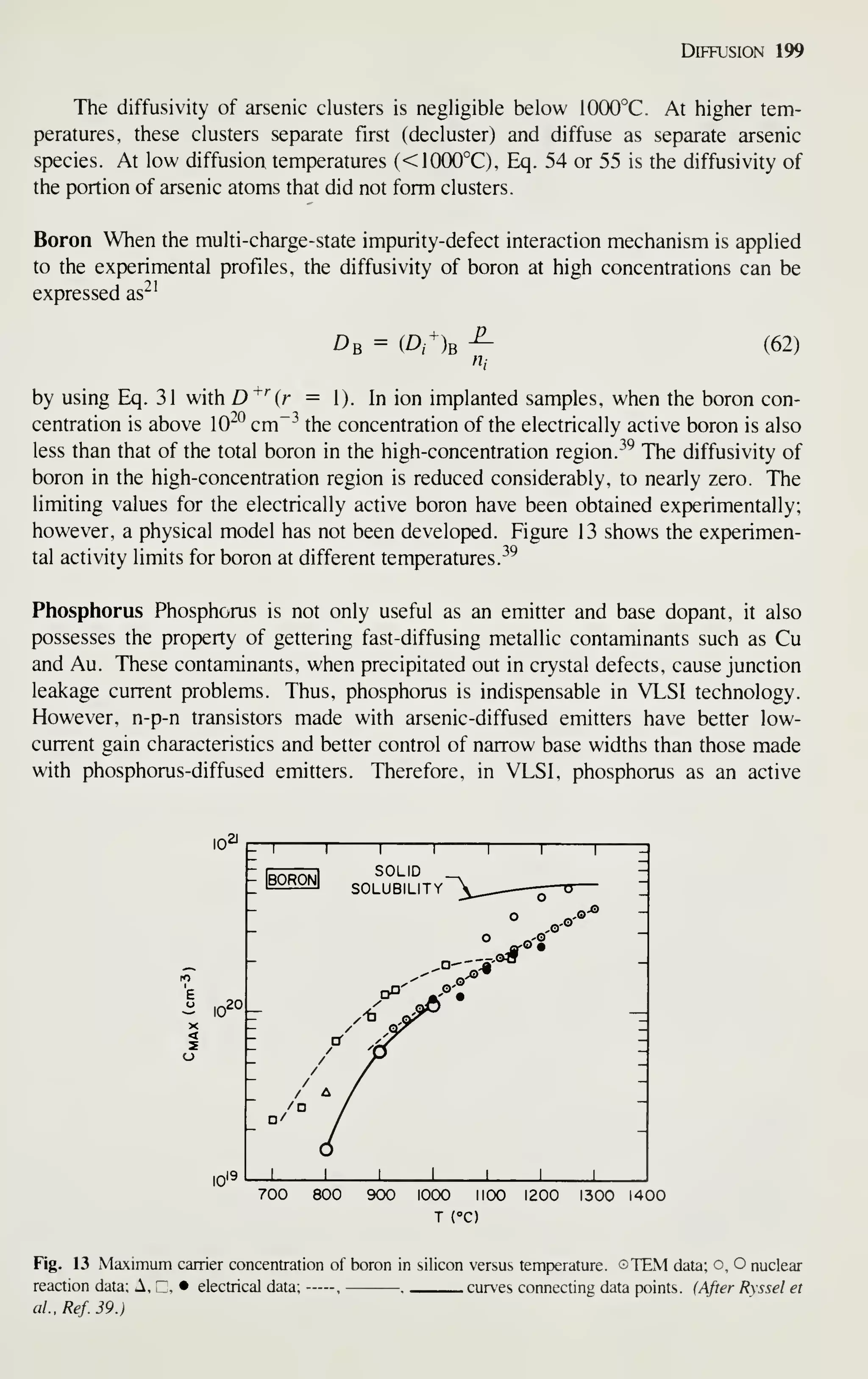
![200 VLSI Technology
TOTAL PHOSPHORUS CONCENTRATION
ELECTRON CONCENTRATION n
P V PAIR DISSOCIATION REGION
D = CONST- n^
.EMITTER DIP
TRANSITION REGION EFFECT
Fig. 14 A model for phosphorus diffusion in silicon. (After Fair, Ref. 21 .)
dopant in small, shallow junctions and low-temperature processing will be limited to
the base dopant of p-n-p transistors and as a gettering agent. Arsenic is the most used
dopant for the source and drain regions in n-channel MOSFETs.
For completeness the diffusion model for phosphorus is discussed briefly. The
characteristic profile of phosphorus can be described as consisting of three regions
(Fig. 14): the high-concentration region, the transition region (often called the
"kink" of the profile), and the low-concentration region (the tail region).
In the high-concentration region, a fraction of the phosphorus ion (P^) pairs with
V^~ vacancies as (PV)~. The concentration of (PV)~ is proportional to n^', the sur-
face electron concentration or the peak concentration for a Gaussian implanted pro-
file. The n^ has to be determined experimentally. The diffusivity of phosphorus Dp,
in this region, is proportional to n ^, the electron concentration, and is
x -I. r» 2
Dp = [Df + or {n/niY] (63)
where
and
Df = 3.85 exp(-3.66/^7) (64)
2-
Z),^- = 44.2 exp(-4.37/;tr) (65)](https://image.slidesharecdn.com/simonm-220913174129-44ec6f82/75/Simon-M-Sze-editor-Very-Large-Scale-Integration-VLSI-Technology-McGraw-Hill-Inc-US-1983-pdf-220-2048.jpg)
![Diffusion 201
Near the transition region, the electron concentration decreases, and when the Fermi
level is close to 0. 1 1 eV below the conduction band edge, the (PV)~ pairs show signi-
ficant dissociations. The electron concentration in this transition region is
n, - 4.65 X 10'' Qxp{0.39 /kT) (66)
The dissociation of (PVy increases the vacancy concentration in the tail region
which can be expressed as
and
iPVr -^ (PVy + e~ (67)
(PVy < => P+ + V- (68)
The arrows shown in Fig. 14 next to (V~) signify that aXn = n^ the excess vacancies
diffuse into both directions from X = Xq. The diffusivity in the tail region increases
as V" is increased and is
^taii = Df + D- -^— [1 + exp(0.3 QV/kT)] (69)
rii Hi
where
D- = 4.44 exp(-4 eW/kT) (70)
The expression for the total phosphorus concentration and the electrically active
phosphorus is
Ct = n + 2.4 X 10"^' «3
(71)
for temperatures between 900 and 1050°C.
Emitter push effect In n-p-n narrow-base transistors using phosphorus-diffused
emitter and boron-diffused base, the base region under the emitter (phosphorus)
region is deeper than that outside the emitter region by 0.2 to 0.6 ixm. This
phenomenon is called the emitter push effect. Since the discovery of this
phenomenon, researchers have proposed various physical mechanisms to explain it.
However, a bandgap narrowing effect together with the phosphorus diffusion model
shown in Fig. 14 adequately explains the emitter push effect. The results are sum-
marized in the following paragraph. However, the derivations of the equations are
omitted.
The dissociation of P^V~~ pairs at the kink region of the phosphorus profile (Fig.
14) provides a mechanism for the enhanced diffusion of phosphorus in the tail region.
The diffusivity of boron under the emitter region (the inner base) is enhanced by the
dissociation of P^ V^~ pairs also. However, at phosphorus concentrations greater than
5 X 10^° atoms/ cm^, misfit between silicon and phosphorus atoms induce a lattice
strain (called the misfit-induced strain) and reduces the concentration of P'^V~~ pairs.](https://image.slidesharecdn.com/simonm-220913174129-44ec6f82/75/Simon-M-Sze-editor-Very-Large-Scale-Integration-VLSI-Technology-McGraw-Hill-Inc-US-1983-pdf-221-2048.jpg)
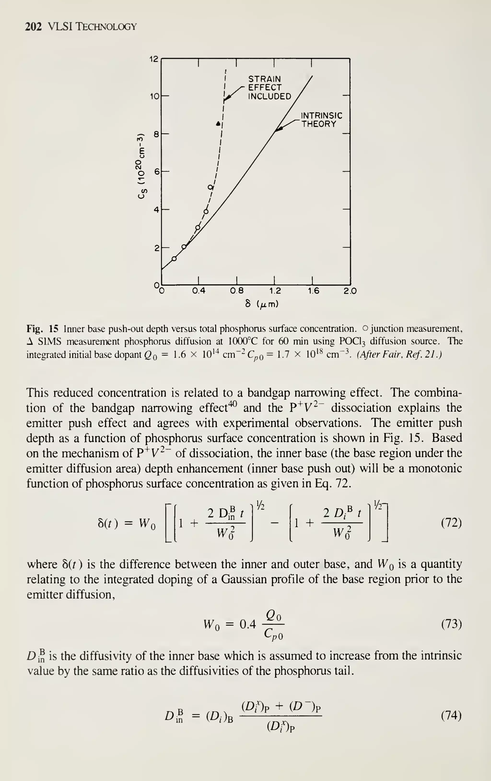
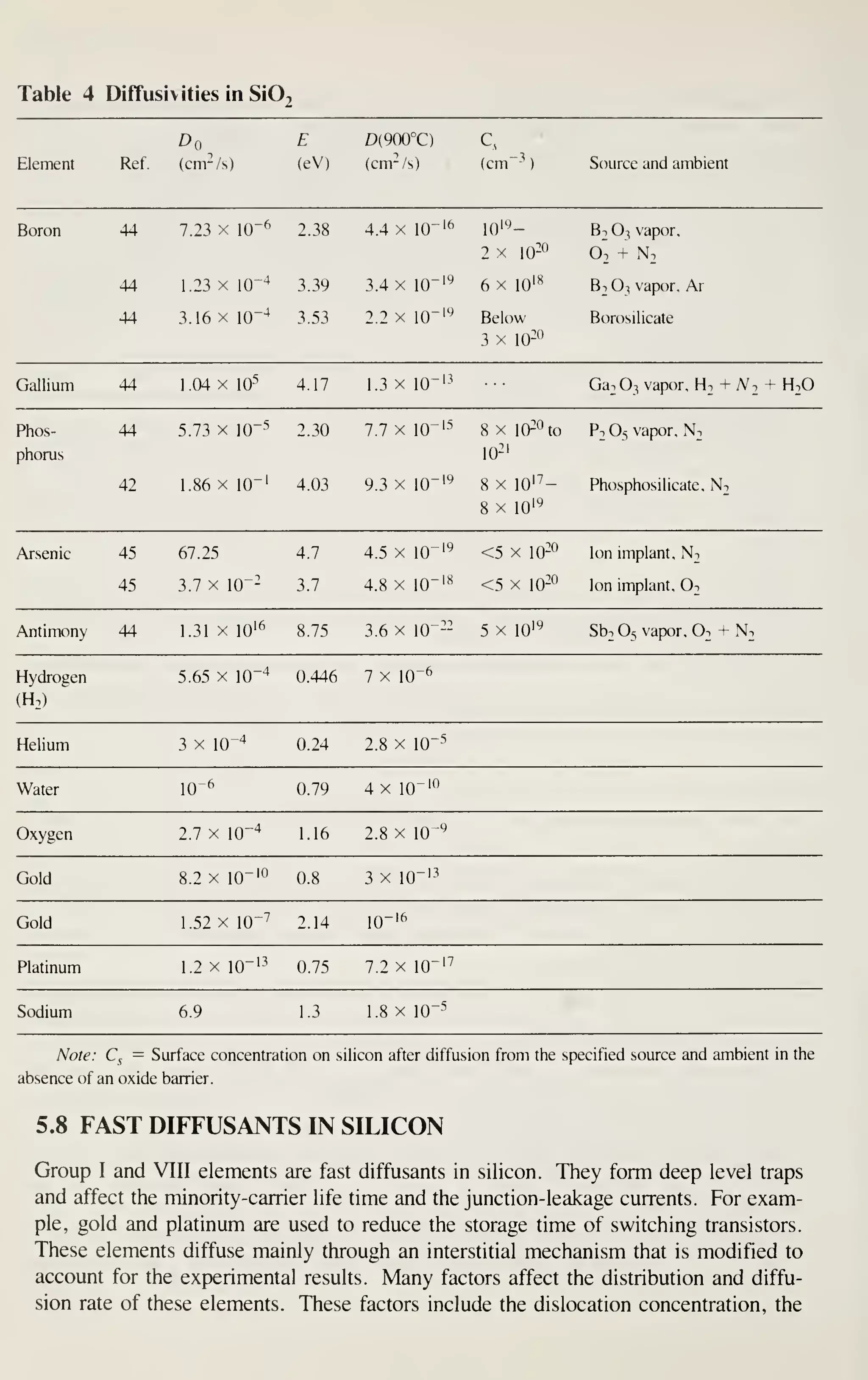
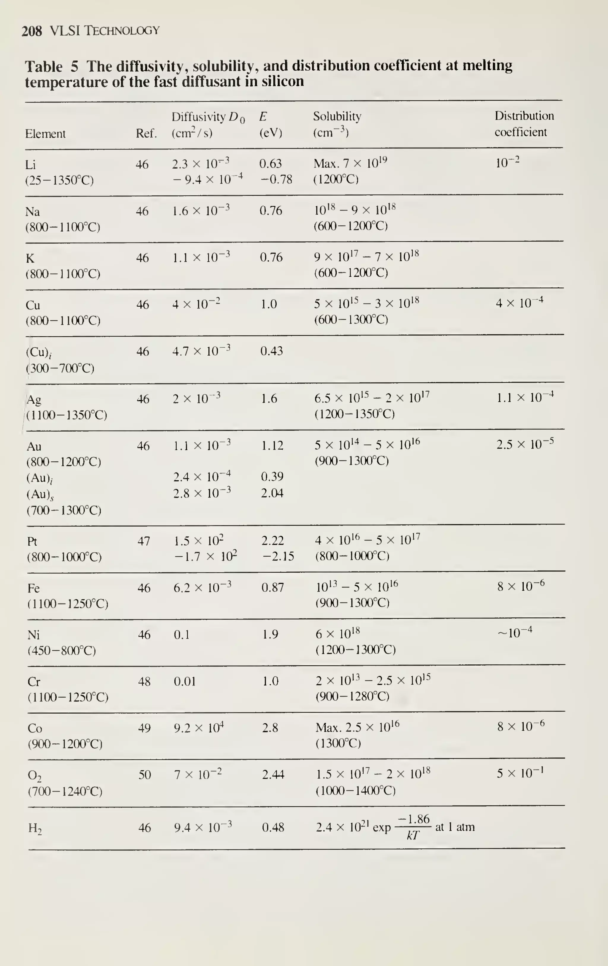
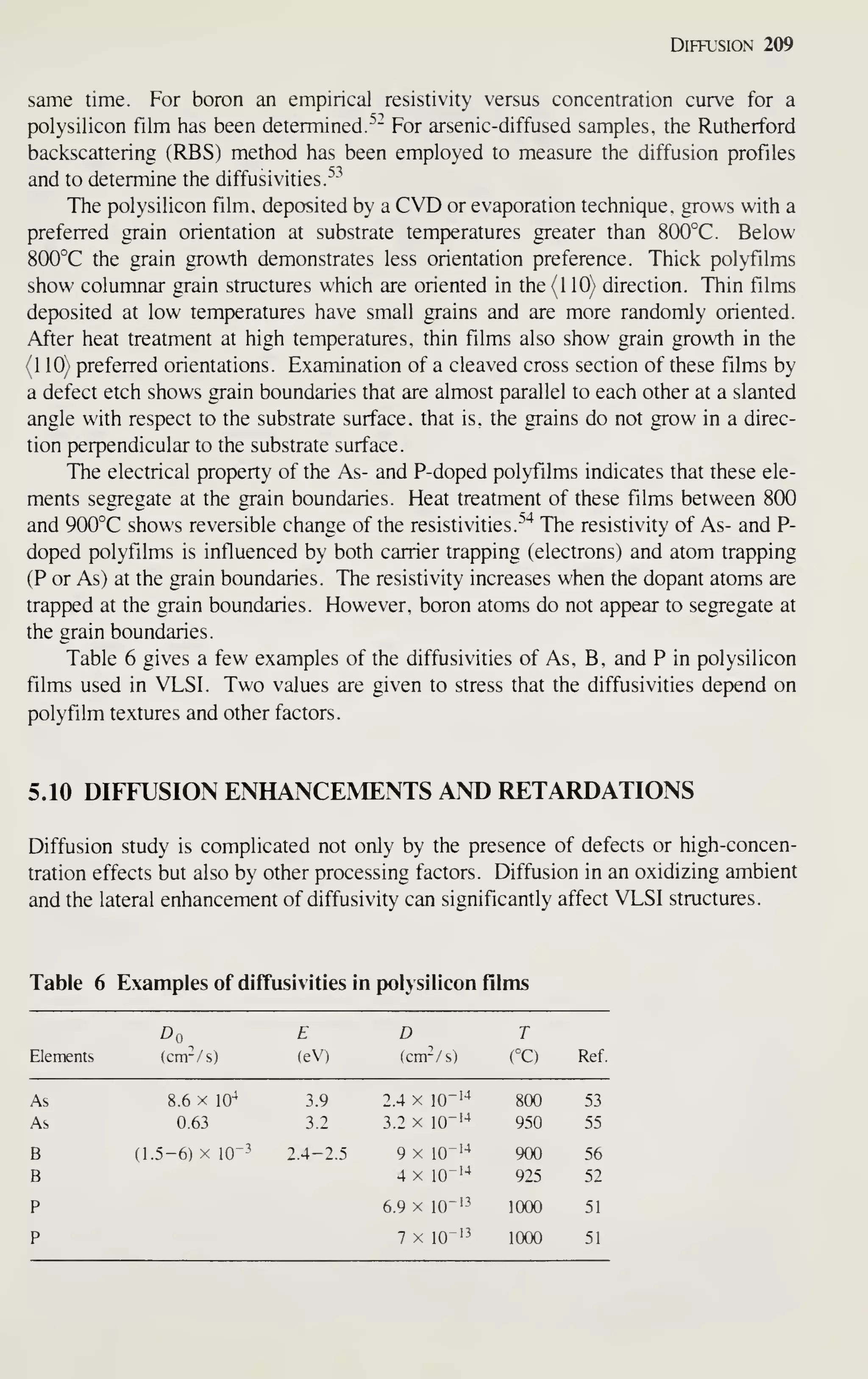
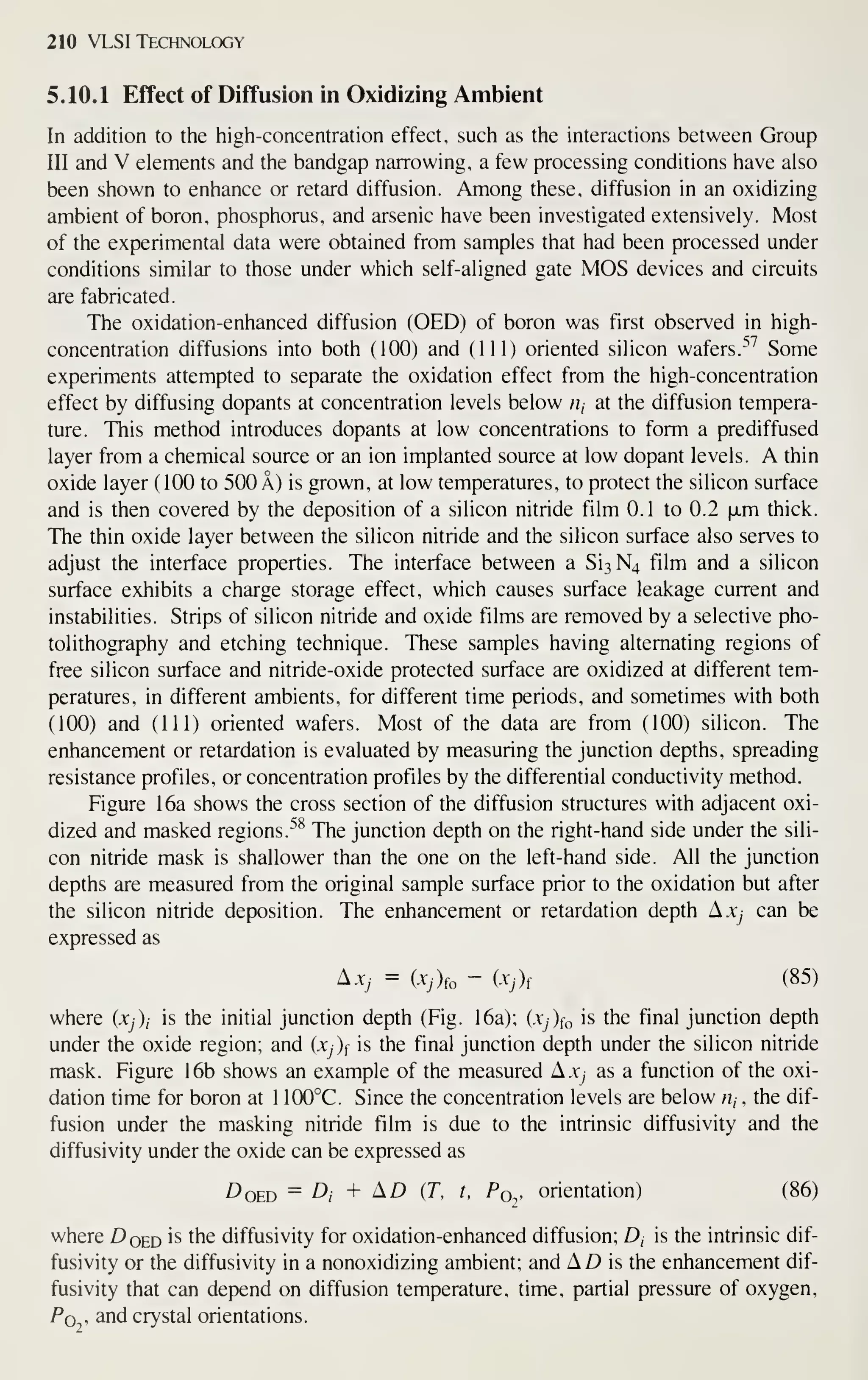
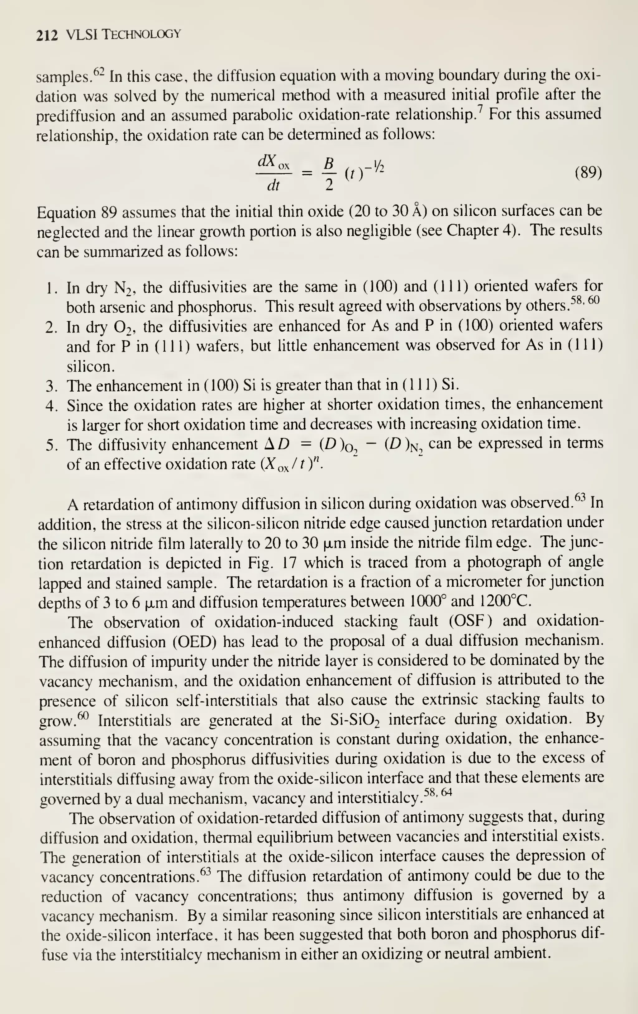
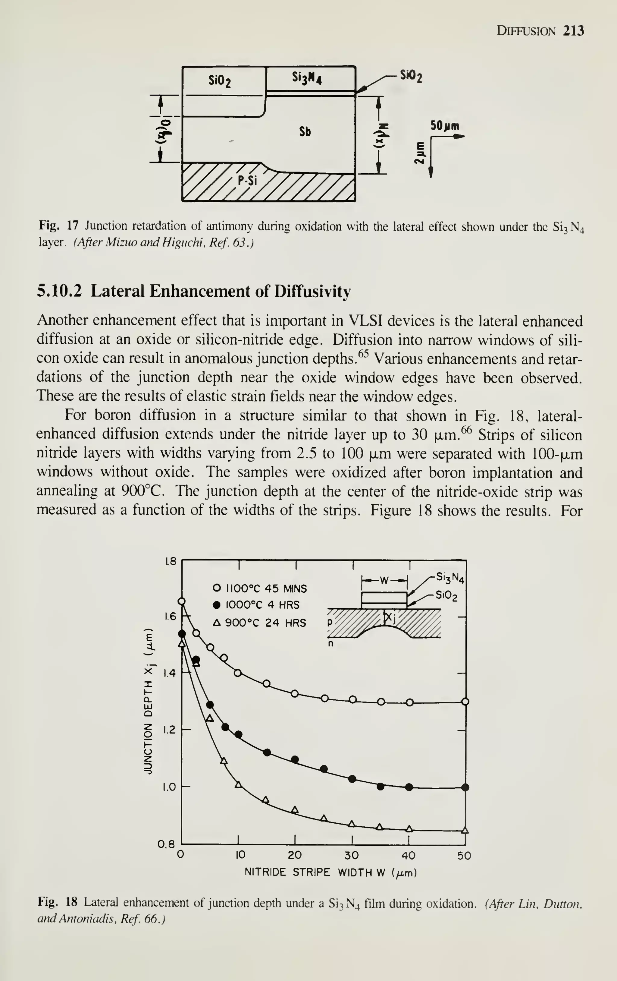
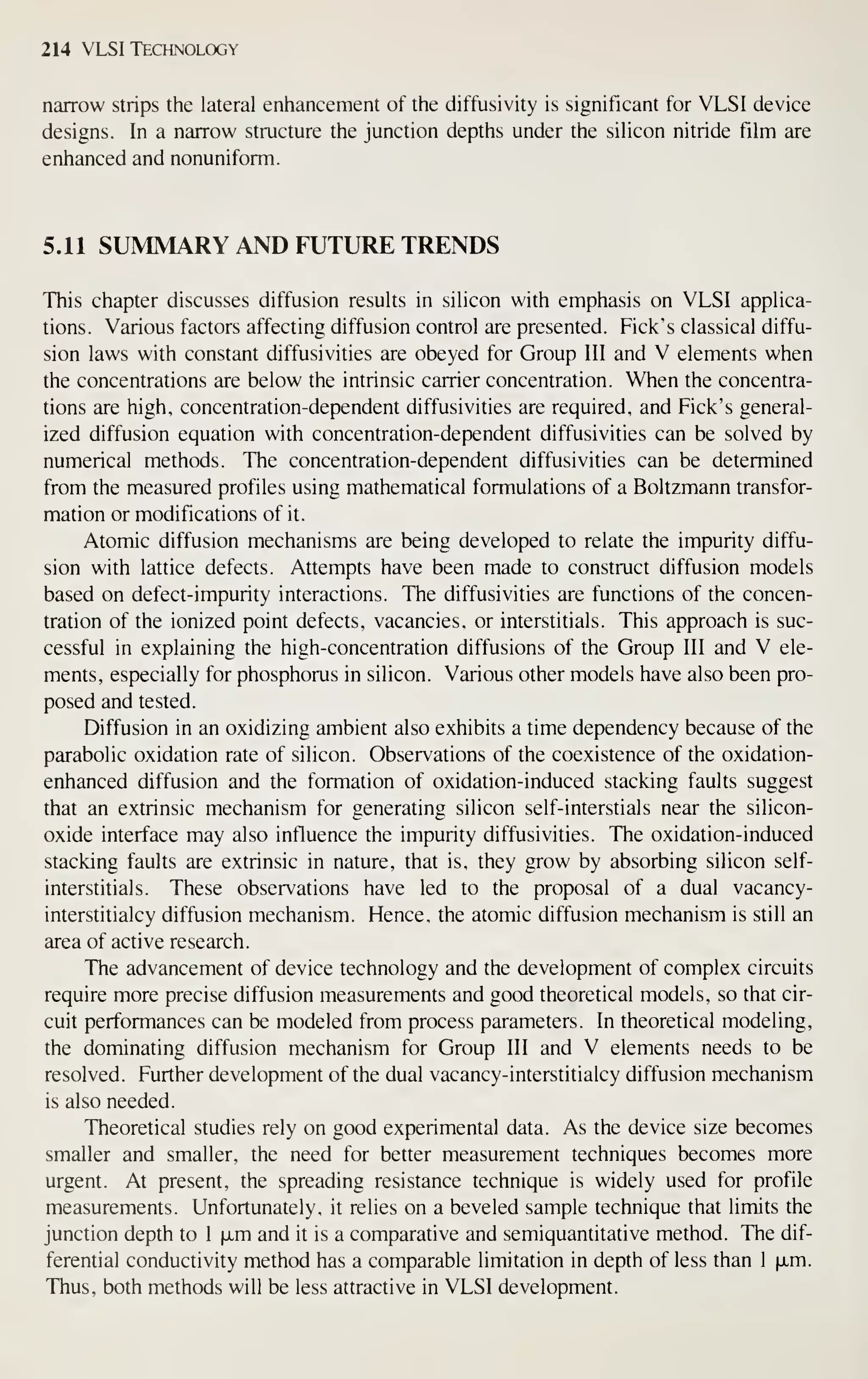
![Diffusion 215
The SIMS analysis is a powerful tool for diffusion profile measurements. It can
measure boron and arsenic concentrations as low as 5 x 10^^ atoms/cm^ and has a
high depth resolution of a few tens of angstroms. Therefore, it is an ideal tool for
measuring shallow diffusion profiles. This technique will provide the needed preci-
sion for profile measurements in VLSI structures.
Conceivably, some pulse annealing procedures for annealing ion implanted
wafers in 5 to 20 s will be developed shortly through the use of an arc-lamp furnace or
a graphite heater in a vacuum environment.^^ Experimental and theoretical investiga-
tions on the effect of temperature transients on the diffusion-annealing properties of
these samples will definitely be addressed soon. Junction depths in the range of 1000
A or less can be realized and the impurity profiles from short period annealing have to
be evaluated. This need points to SIMS analysis technique again and further develop-
ment of this technique is required.
REFERENCES
[1] W. G. Pfann, Semiconductor Signal Translating Device, U.S. Patent No. 2,597,028 (1952).
[2] B. Tuck, "Introduction to Diffusion in Semiconductors," lEEMono. Ser., Lotuion, 16 1 19 (1974).
[3] A. Pick, Ann. Phys. Leipzig, 170, 59 (1855).
[4] J. Crank. The Mathematics ofDiffusion, Oxford University Press, London, 1957.
[5] B. I. Boltaks, Diffiision in Semiconductors, Academic, New York, 1963.
[6] E. C. Douglas and A. G. F. Dingwall, "Ion Implantation For Threshold Control in COSMOS Cir-
cuits," IEEE Trans. Electron Devices, ED-21. 324 (1974).
[7] G. Masetti, P. Negrini, S. Solmi, and G. Soncini, "Boron Drive-in in Silicon in Oxidizing Atmos-
phere." A/rafre^., 42, 346(1973).
[8] M. Ghezzo, "Diffusion from a Thin Layer into a Semi-Infinite Medium with Concentration Dependent
Diffusion Coefficient," J. Electrochem. Soc. 119, 977 (1972).
[9] M. Ghezzo, "Diffusion from a Thin Layer into a Semi-Infinite Medium with Concentration Dependent
Diffusion Coefficient, Part II," J. Electrochem. Soc. 120, 1 123 ( 1973).
[10] R. B. Fair and J. C. C. Tsai, "The Diffusion of Ion Implanted Arsenic in Silicon," J. Electrochem.
Soc, 122, 1689(1975).
[11] P. G. Shewmon, Diffusion in Solids, McGraw-Hill, New York, 1963.
[12] U. Gosele and H. Strunk, "High Temperature Diffusion of Phosphorus and Boron in Silicon Via
Vacancies or Via SelfInterstitials?" Appl. Phys., 20, 265 (1979).
[13] R. L. Longini and R. F. Green, "Ionization Interaction Between Impurities in Semiconductors and
Insulators," Phys. Rev., 102. 992 (1956).
[14] F. J. Morin and J. P. Malta, "Electrical Properties of Silicon Containing Arsenic and Boron," Phys.
Rev.,96.2S{954).
[15] D. Shaw, "Self and Impunty Diffusion in Ge and Si," PM5.5r«m.?5oMfi, 72, 11 (1975).
[16] G. D. Watkins, J. R. Troxell, and H. P. Chatteijee, "Vacancies and Interstitials in Silicon," Inst.
Phys. Conf. Ser., 46, 16 (1979).
[17] R. E. Whan and F. L. Vook, "Infrared Studies of Defect Production in N-Type Silicon: Irradiation-
Temperature Dependence," Phys. Rev., 153, 814 ( 1967).
[18] L. C. Kimerling, P. Blood, and W. M. Gibson, "Defect States in Proton-Bombarded Silicon at T <
300 K," Inst. Phys. Conf. Ser., 46, 273 (1979).
[19] J. G. De Wit, C. A. J. Ammerlaan, and E. G. Sieverts, "An ENDOR Study of the Divacancy in Sili-
con," Inst. Phys. Conf Ser., 23, 178 (1975).
[20] J. C. Bourgoin, "Ionization Effects on Impurity and Defect Migration in Semiconductors," Inst. Phys.
Conf. Ser., 23,149(1915).](https://image.slidesharecdn.com/simonm-220913174129-44ec6f82/75/Simon-M-Sze-editor-Very-Large-Scale-Integration-VLSI-Technology-McGraw-Hill-Inc-US-1983-pdf-235-2048.jpg)
![Diffusion 217
[48] W. Wurker, K. Roy, and J. Hesse. "Diffusion and Solid Solubility of Chromium in Silicon,"" Mater.
Res. Bull.. (U.S.A.), 9, 971 (1974).
[49] H. Kitagano and K. Hashimoto, "Diffusion Coefficient of Cobalt in Silicon," J. Appl. Phxs. Jpn.. 16,
173(1977).
[50] J. C. Mikkelsen, Jr., "Diffusivity of Oxygen in Silicon During Steam Oxidation," Appl. Phys. Lett.,
40,336(1982).
[51] T. I. Kamins, J. Manolin, and R. N. Tucker, "Diffusion of Impurities in Polycrystalline Silicon,"' J.
Appl. Phys.. 43, ^3 (1912).
[52] C. J. Coe, "The Lateral Diffusion of Boron in Polycrystalline Silicon and Its Influence on the Fabrica-
tion of Sub-Micron Mosts." Solid State Electron.. 20, 985 (1977).
[53] B. Swaminathan, K. C. Saraswat, R. W. Dutton. and T. I. Kamins, "Diffusion of Arsenic in Poly-
crystalline Silicon,"" Appl. Phys. Lett., 40, 795 (1982).
[54] M. M. Mandurah, K. C. Saraswat, C. R. Helms, and T. I. Kamins, "Dopant Segregation in Polycrys-
talline Silicon,"" y. Appl. Phys., 51, 5755 (1980).
[55] K. Tsukamoto, Y. Akasaka, and K. Horie, "Arsenic Implantation into Polycrystalline Silicon and Dif-
fusion to Silicon Substrate," J. Appl. Phys.. 48. 1815 ( 1977).
[56] S. Horiuchi and R. Blanchard, "Boron Diffusion in Polycrystalline Silicon Layers,"" Solid State Elec-
tron.. 18.529(1975).
[57] W. G. Allen and K. V. Anand. "Orientation Dependence of the Diffusion of Boron in Silicon,"' Solid
State Electron.. 14. 397 (1971).
[58] K. Taniguchi. K. Kurosawa, and M. Kashiwagi, "Oxidation Enhanced Diffusion of Boron and Phos-
phorus in ( 100) Silicon,"" y. Electrochem. Soc, 127, 2243 (1980).
[59] S. M. Hu, "Formation of Stacking Faults and Enhanced Diffusion in the Oxidation of Silicon,"' J.
Appl. Phys., 45, 1567(1974).
[60] A. M. R. Lin, D. A. Antoniadis, and R. W. Dutton, "The Oxidation Rate Dependence of Oxidation-
Enhanced Diffusion of Boron and Phosphorus in Silicon," J. Electrochem. Soc, 128, 1 131 (1981 ).
[61] D. A. Antoniadis, A. M. Lin. and R. W. Dutton. "Oxidation-Enhanced Diffusion of Arsenic and
Phosphorus in Near Intrinsic^OO) Silicon." Appl. Phys. Lett., 33, 1030 (1978).
[62] Y. Ishikawa, Y. Sakina, H. Tanaka, S. Matsumoto, and T. Niimi, "The Enhanced Diffusion of
Arsenic and Phosphorus in Silicon by Thermal Oxidation,'" 7. Electrochem. Soc, 129, 644 ( 1982).
[63] S. Mizuo and H. Higuchi, "Retardation of Sb Diffusion in Si During Thermal Oxidation,"" J. Appl.
Phys. Jpn.. 20, 1?>9{9S).
[64] T. Y. Tan and U. Gosele, "Oxidation-Enhanced or Retarded Diffusion and the Growth or Shrinkage
of Oxidation-Induced Stacking Faults in Silicon," /ip/?/. Phys. Lett., 40. 616 ( 1982).
[65] C. F. Gibbon. E, I. Povilonis, and D. R. Ketchow. "The Effect of Mask Edges on Dopant Diffusion
into Semiconductors."" J. Electrochem. Soc. 119. 767 (1972).
[66] A. M. Lin, R. W. Dutton, and D. A. Antoniadis, "The Lateral Effect of Oxidation on Boron Diffusion
in(lOO) Silicon,"" Appl. Phys. Lett., 35, 799 ( 1979).
[67] D. F. Downey, C.J. Russo, and J. T. White, "Activation and Process Characteristics of Infrared
Rapid Isothermal and Furnace Annealing Techniques,"' Solid State Technol., 25, No. 9, 87 ( 1982).
PROBLEMS
1 (a) Derive expressions of concentration gradients for the erfc and Gaussian distributions. If the substrate
doping density is C^^b' derive the expressions of the junction depths.
fZ?) Assuming C, = lO'^ cm"^^ for an erfc distribution and 5 = 1 x lO'^ atoms/cm- for a Gaussian
distribution, C^ub = lO'"' atoms/cm and D = 1 x 10"'-^ cm-/s (which is close to the boron diffusivity
at 9(X)°C), calculate the junction depths and the concentration gradients for both distributions. Calculate the
integrated dopants for the erfc distribution and the surface concentration for the Gaussian distribution for dif-
fusion times of 10, 30, and 60 min.
(c) Compare and discuss the results of (a) and (b).](https://image.slidesharecdn.com/simonm-220913174129-44ec6f82/75/Simon-M-Sze-editor-Very-Large-Scale-Integration-VLSI-Technology-McGraw-Hill-Inc-US-1983-pdf-237-2048.jpg)
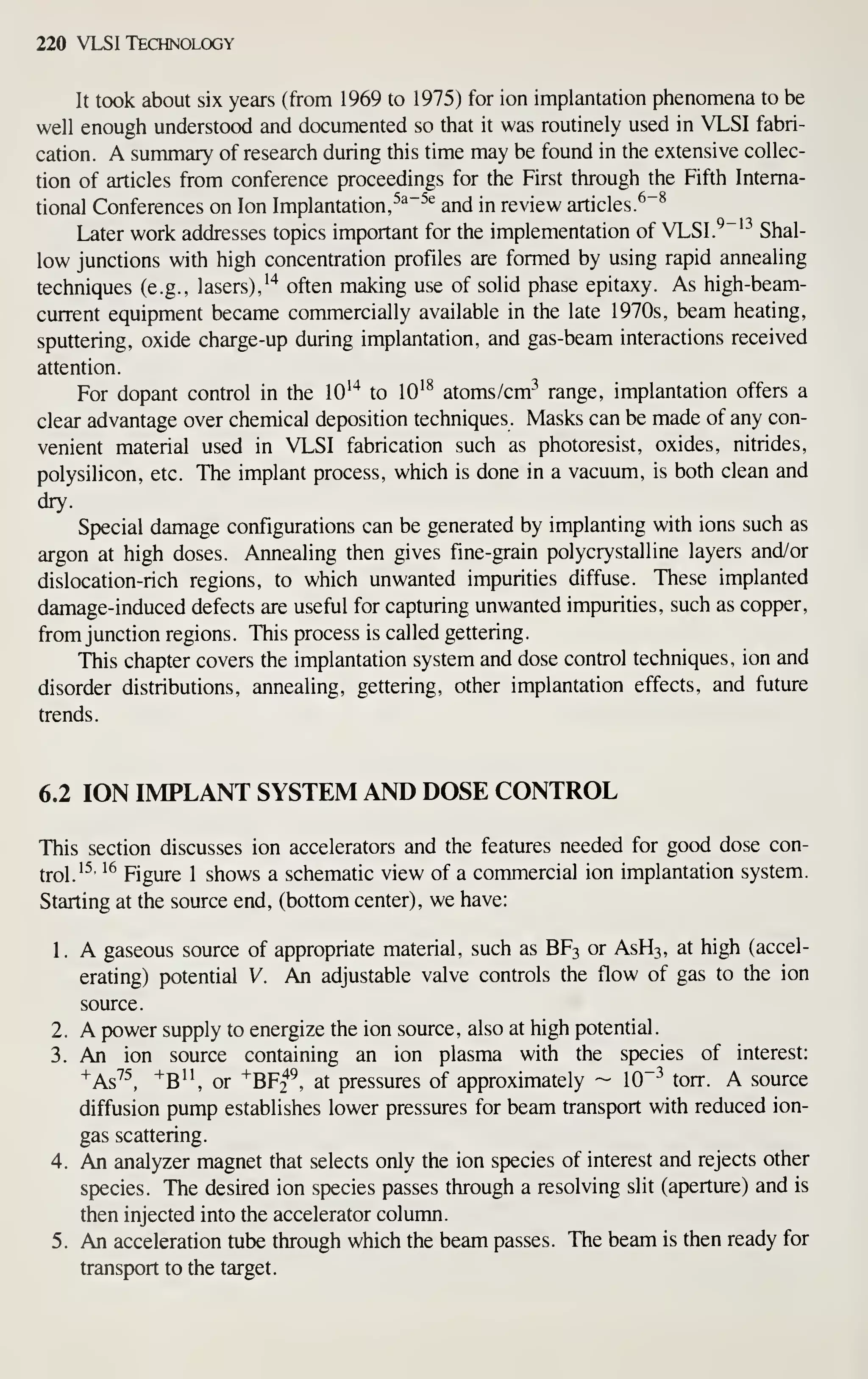
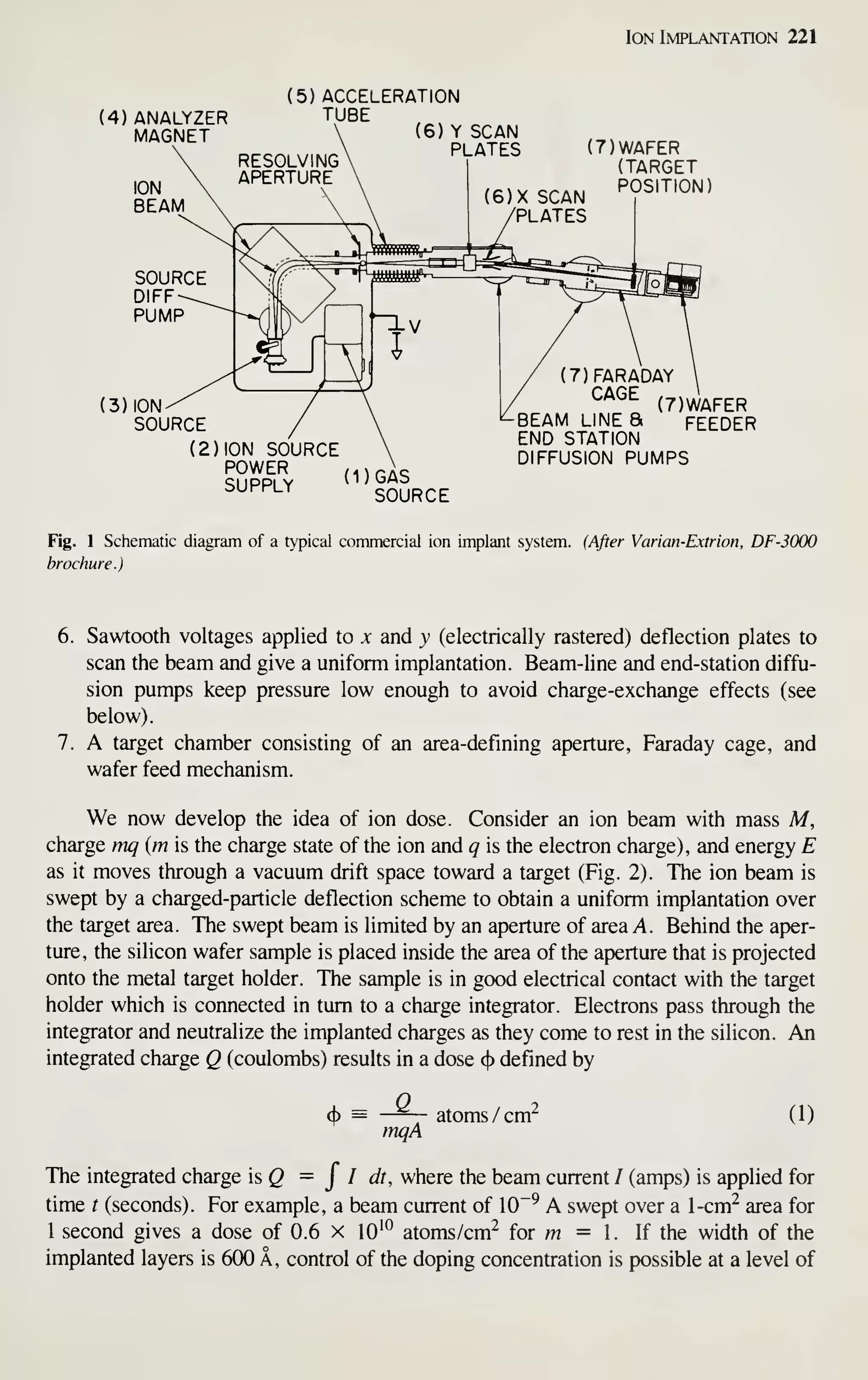
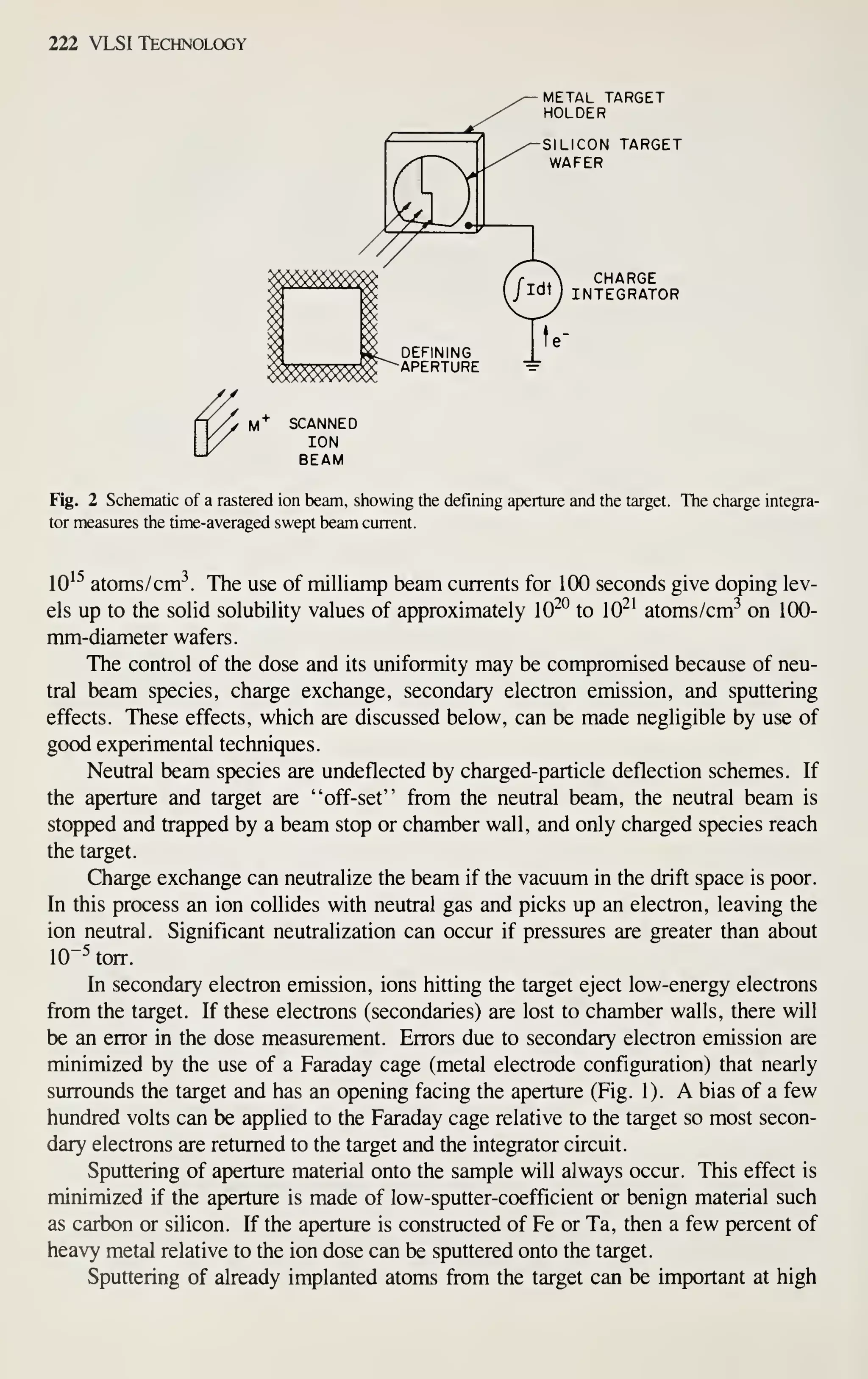
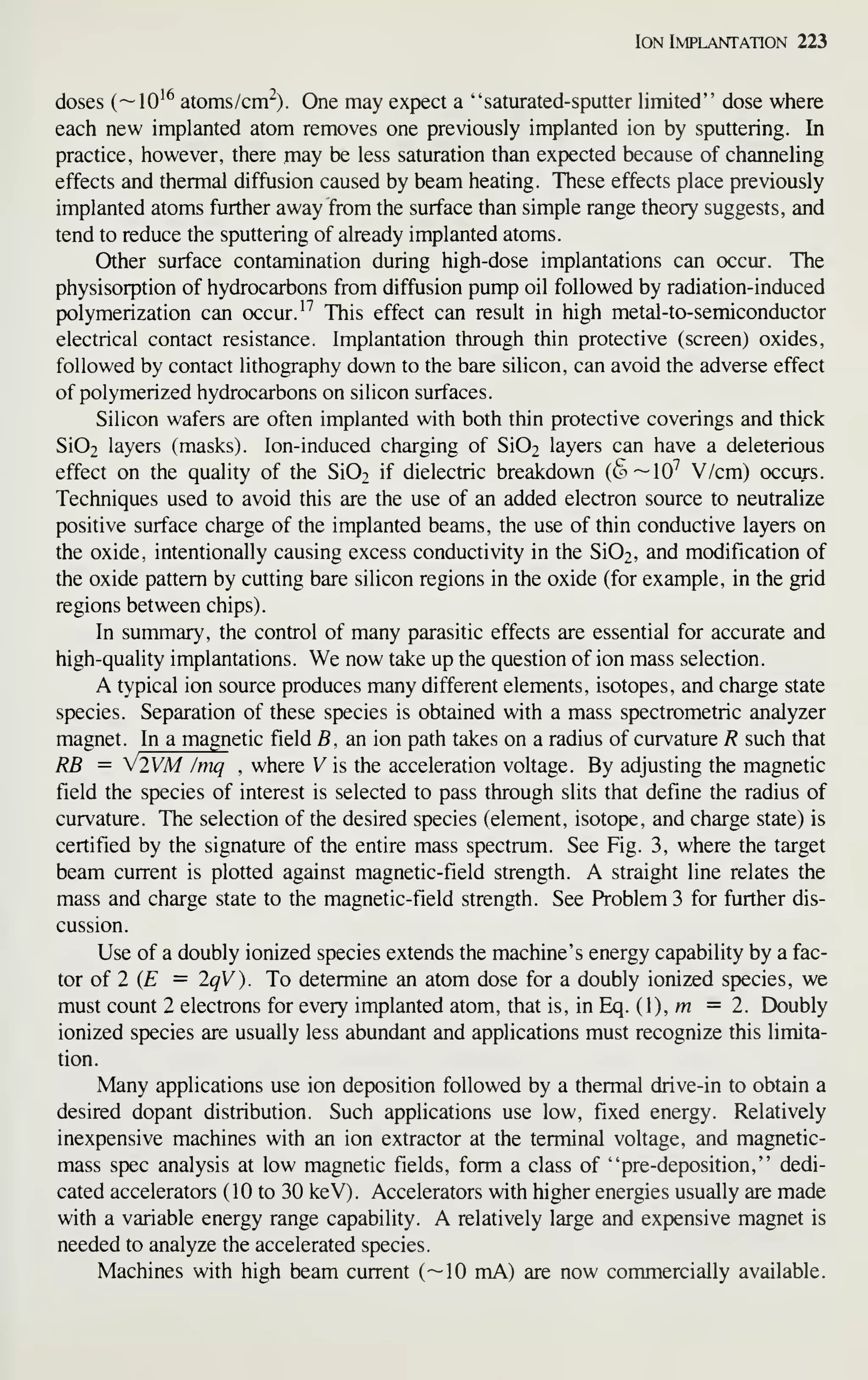
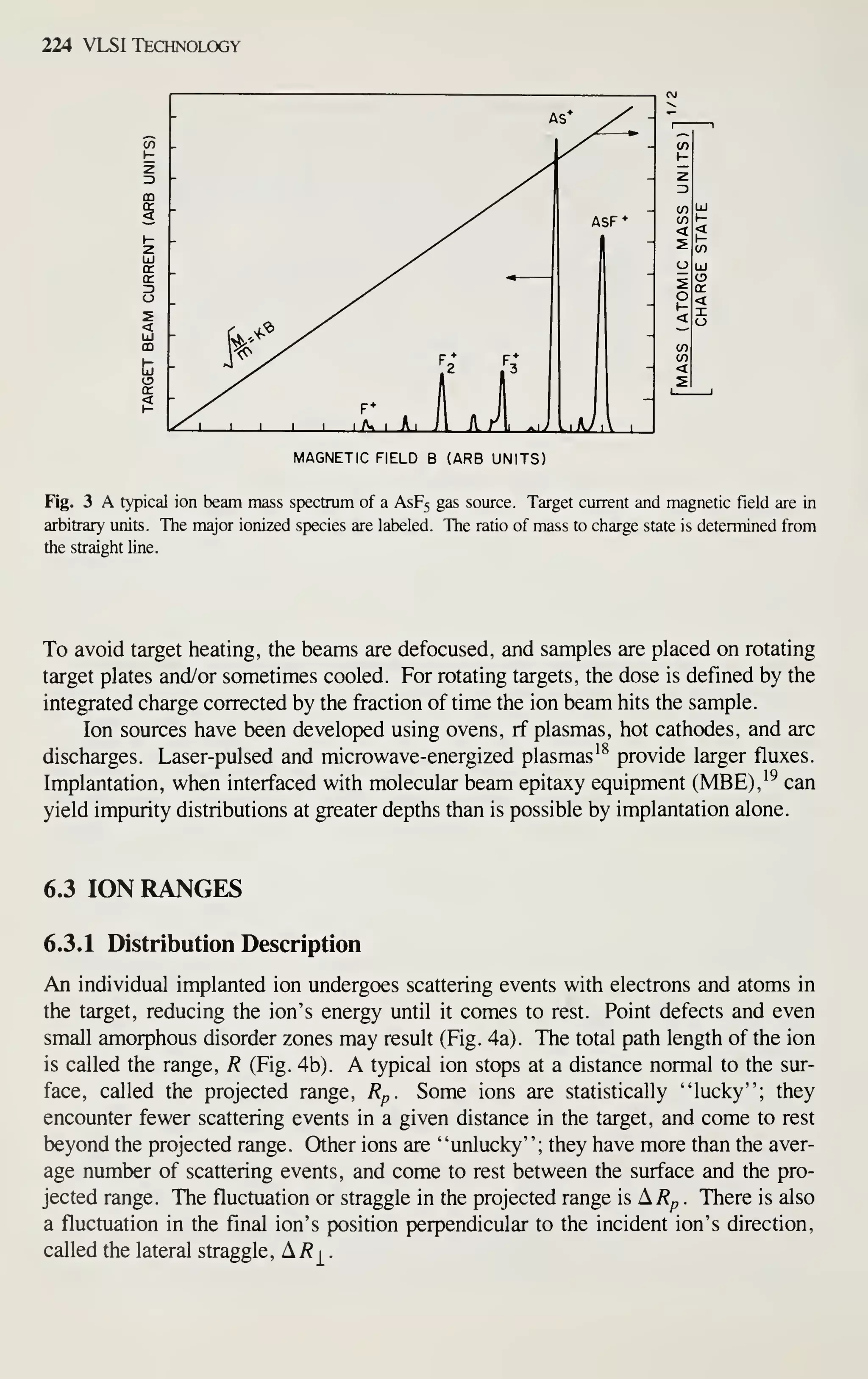
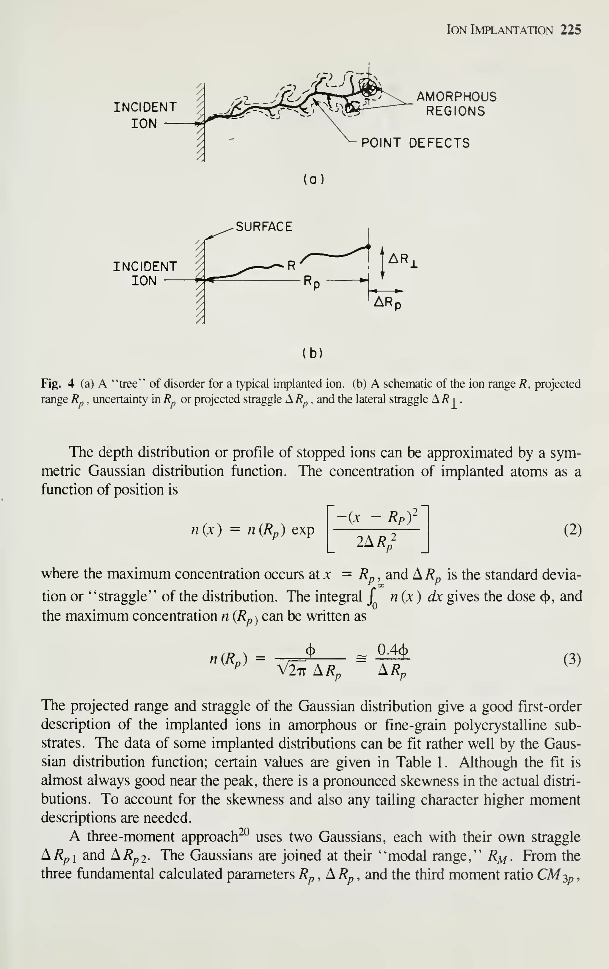
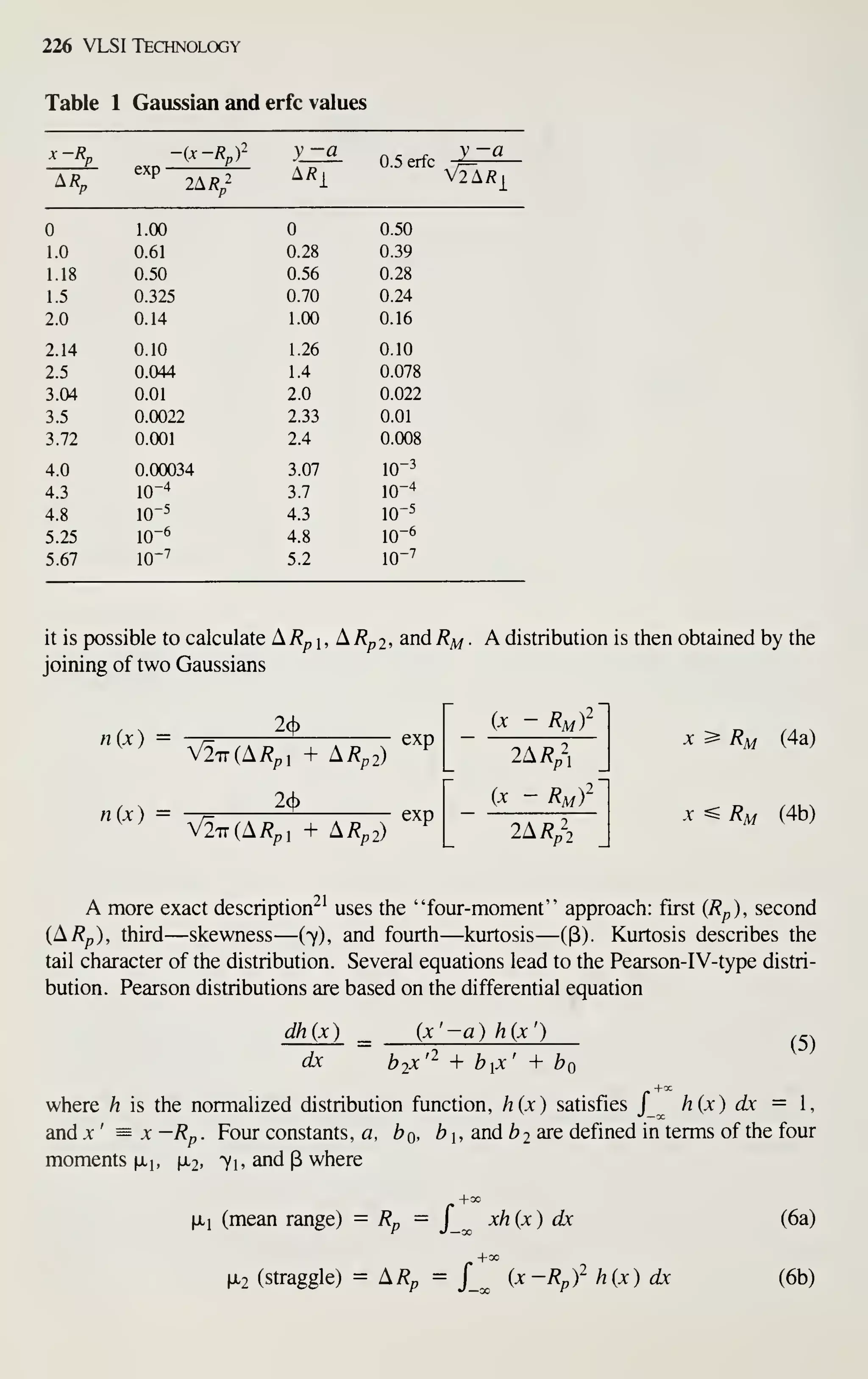
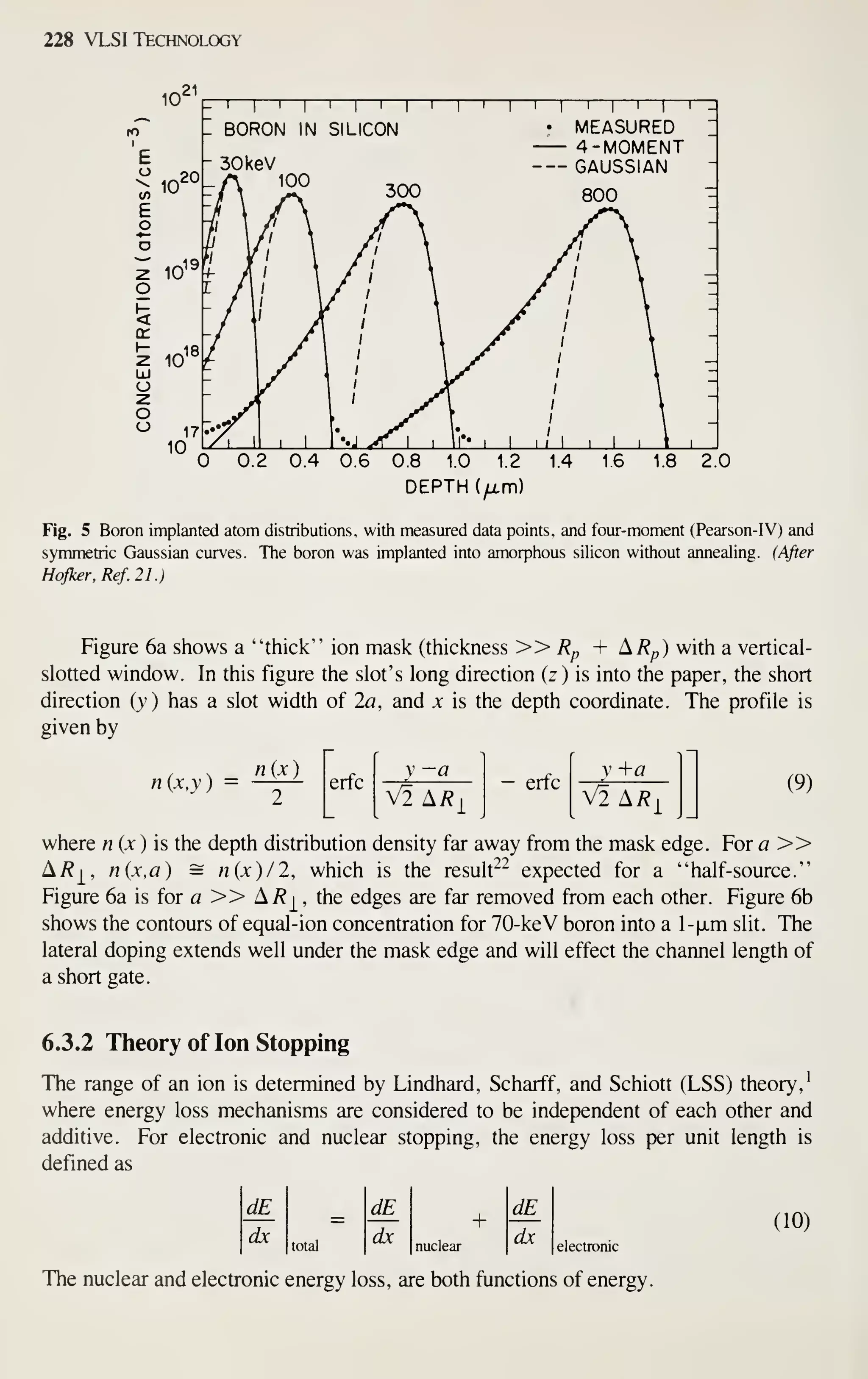
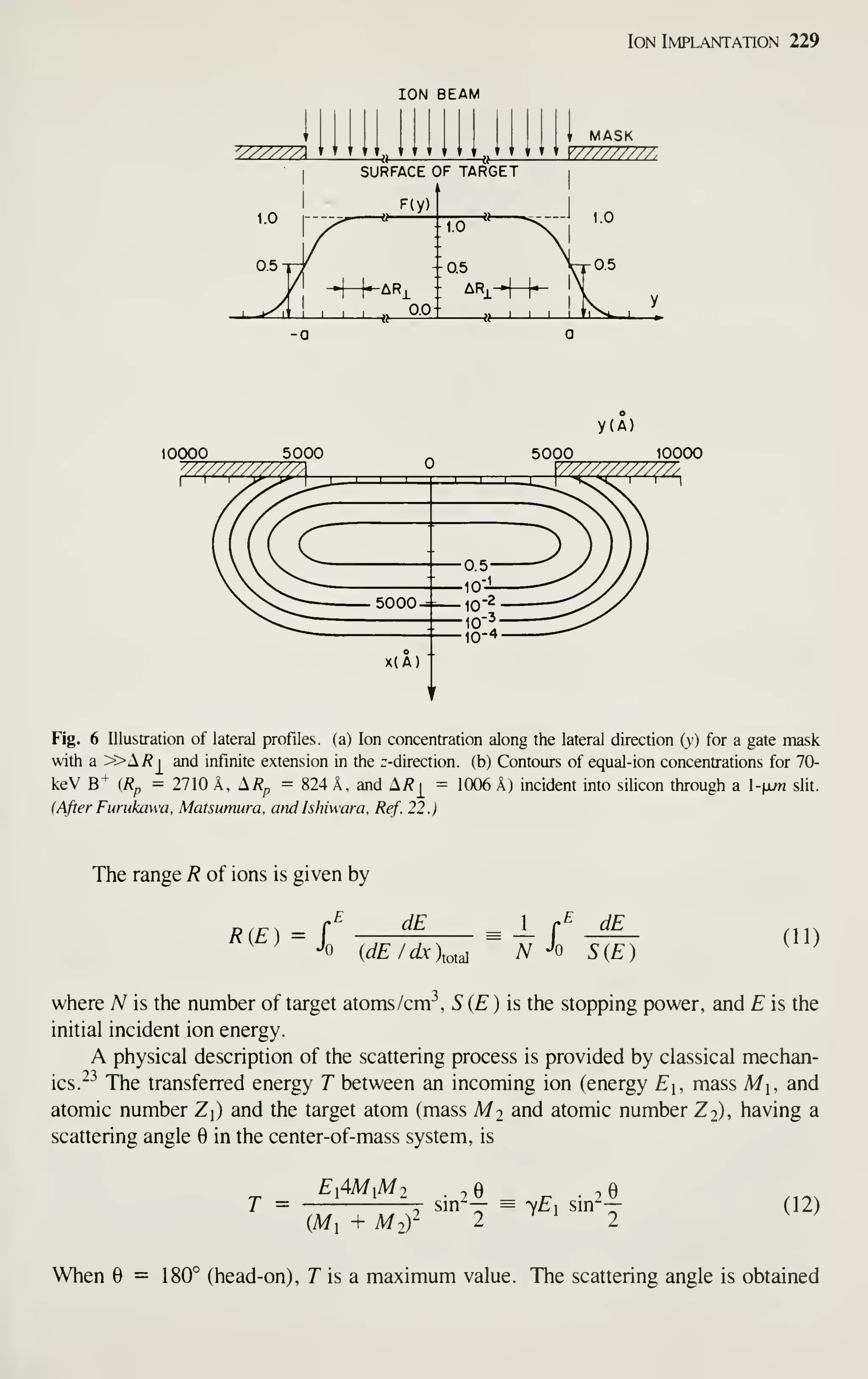
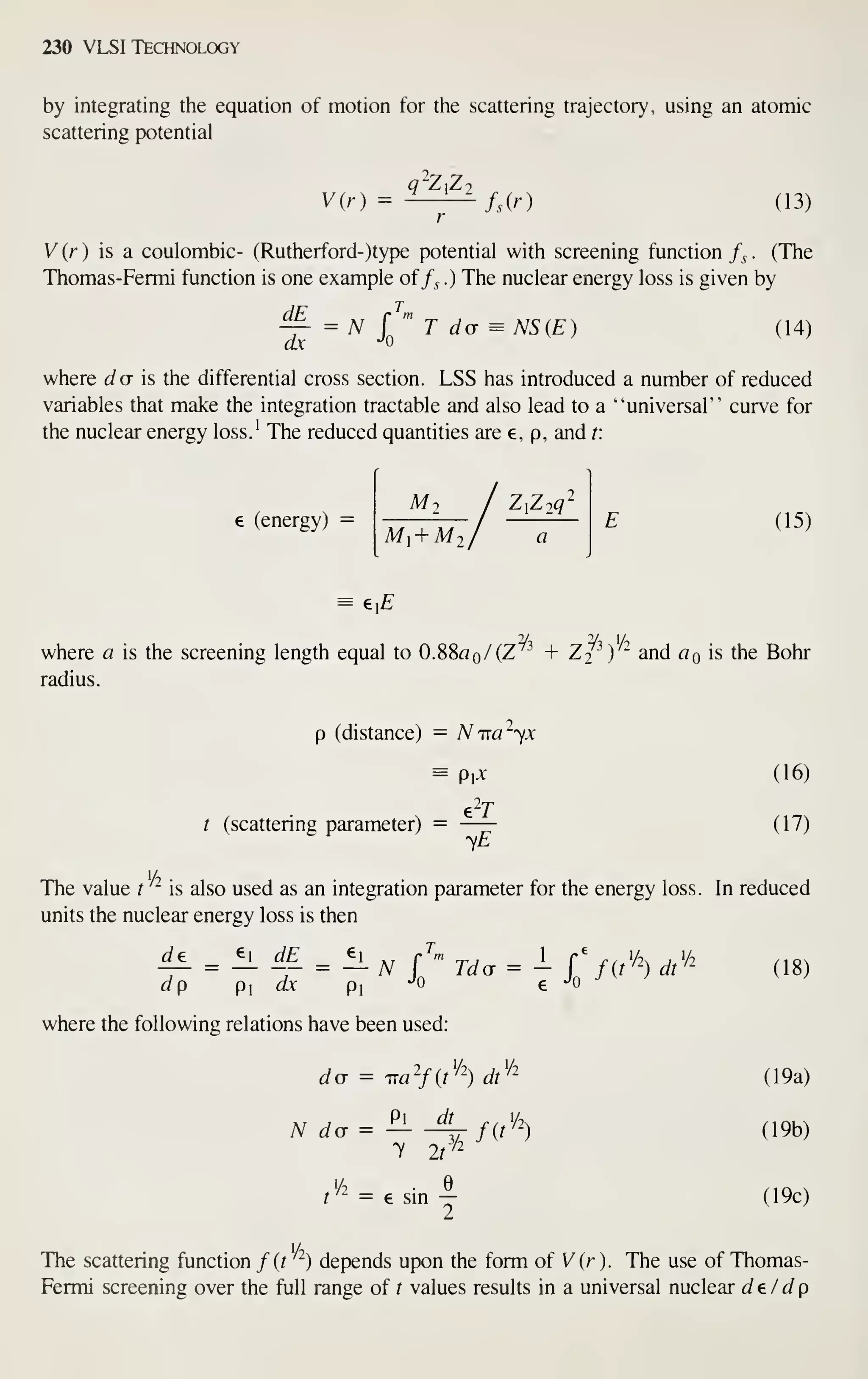
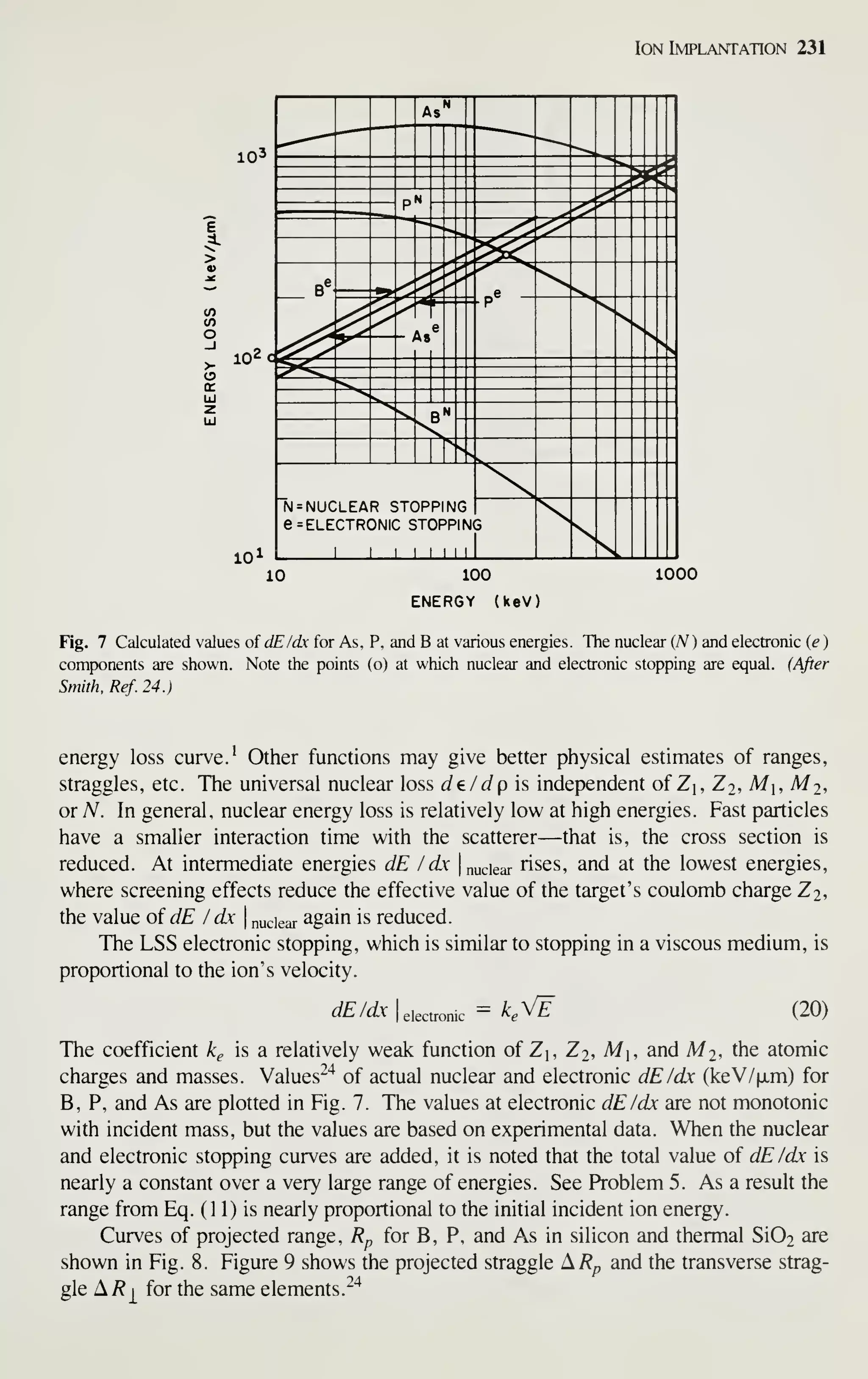
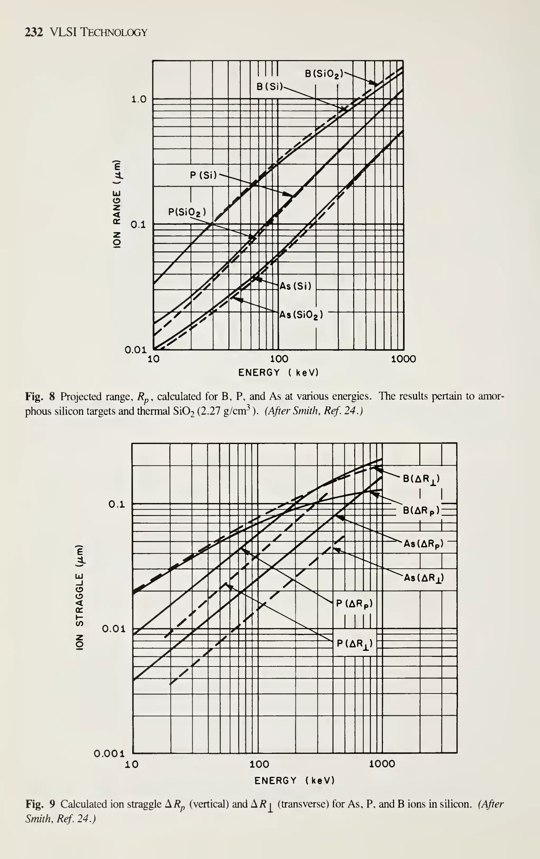
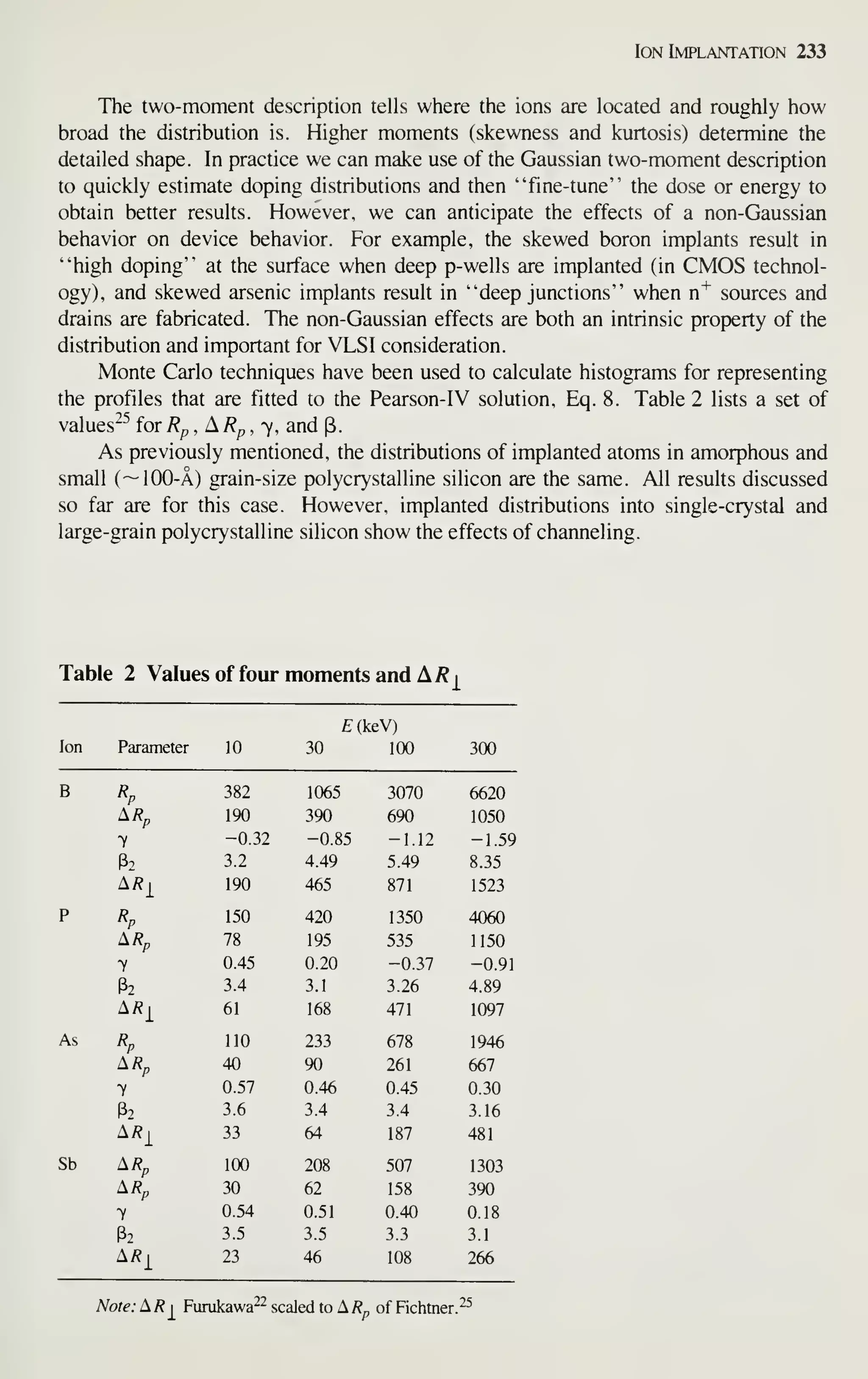
![234 VLSI Technology
6.3.3 Ion Channeling
Channeling starts to occur when an incident ion finds entry into an open space
between rows of atoms. "^ Once the ion is inserted, steering forces of the atomic row
potentials become operative and steer the ion toward the center of the open space
(channel). The ion is stably guided along the channel over considerable distances.
The ion gradually loses energy through its gentle, glancing collisions on the edges of
the channel, and eventually scatters out of the channel. Channeled penetration dis-
tances can be several times the penetration in amorphous targets, because the energy
loss for channeled ions is low compared with non-channeled ions. If attempts are
made to avoid channeling in single crystal silicon targets by the orientation to dense
atom directions (e.g., the (763)) then channeling effects are minimized but not elim-
inated (Fig. 10).
Profiles obtained by implantation into single crystals in such a way as to avoid
channeling are characterized by tails of atoms [as determined by careful secondary ion
mass spectroscopy, or SIMS (see Chapter 12) and tails of free charge doping (as
determined by electrical data)] . The channeling tails often can be fit to an exponen-
tial function of position, exp( —x I ), where is typically found to be —0. 1 fxm. The
tails are more prominent for phosphorus than for boron because the acceptance or crit-
ical angle for channeling is larger for heavier atoms. The critical angle is proportional
to z/-. For 50-keV phosphorus, il^crit
= 5.9°, while for 50-keV boron, i|;crit
~ 4.8°
along the (110) axis. The critical angle (for relatively high energies)^^ is given by
^crit =
IZxZiq^
Ed
'/2
(21)
where d is the atomic spacing along the aligned row.
The primary mechanism for tail formation in crystalline targets that are oriented
off major axes is believed to be channeling into major axes. (An alternate proposal
invokes an interstitial diffusion mechanism at implantation temperatures.) Experi-
ments with phosphorus prove that the tail of the distribution is due to channeling.
^^
Transmission of phosphorus ions through thinned silicon shows that ions emerge with
measurable energies and therefore are unambiguously channeled. The crystals are
about 0.5 |JLm thick and implanted with radioactive P-^^. The ions corresponding to the
INCIDENT /
DIRECTION
<763>
RANDOM
DECHANNELED
Fig. 10 Schematic diagram of an ion path in a single crystal for an ion incident in a "dense" (763) direc-
tion. The path shown has non-channeled and channeled behavior.](https://image.slidesharecdn.com/simonm-220913174129-44ec6f82/75/Simon-M-Sze-editor-Very-Large-Scale-Integration-VLSI-Technology-McGraw-Hill-Inc-US-1983-pdf-254-2048.jpg)
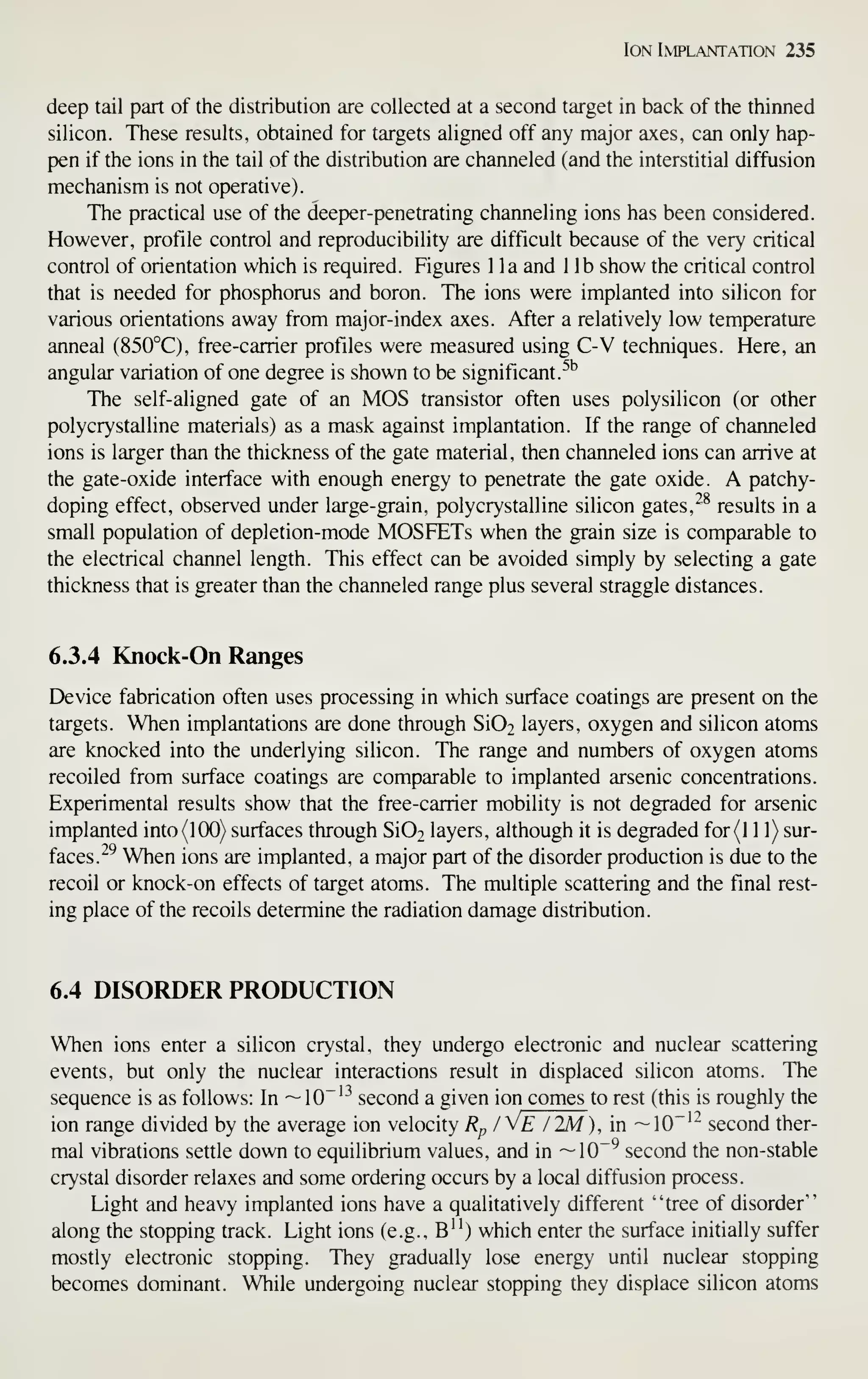
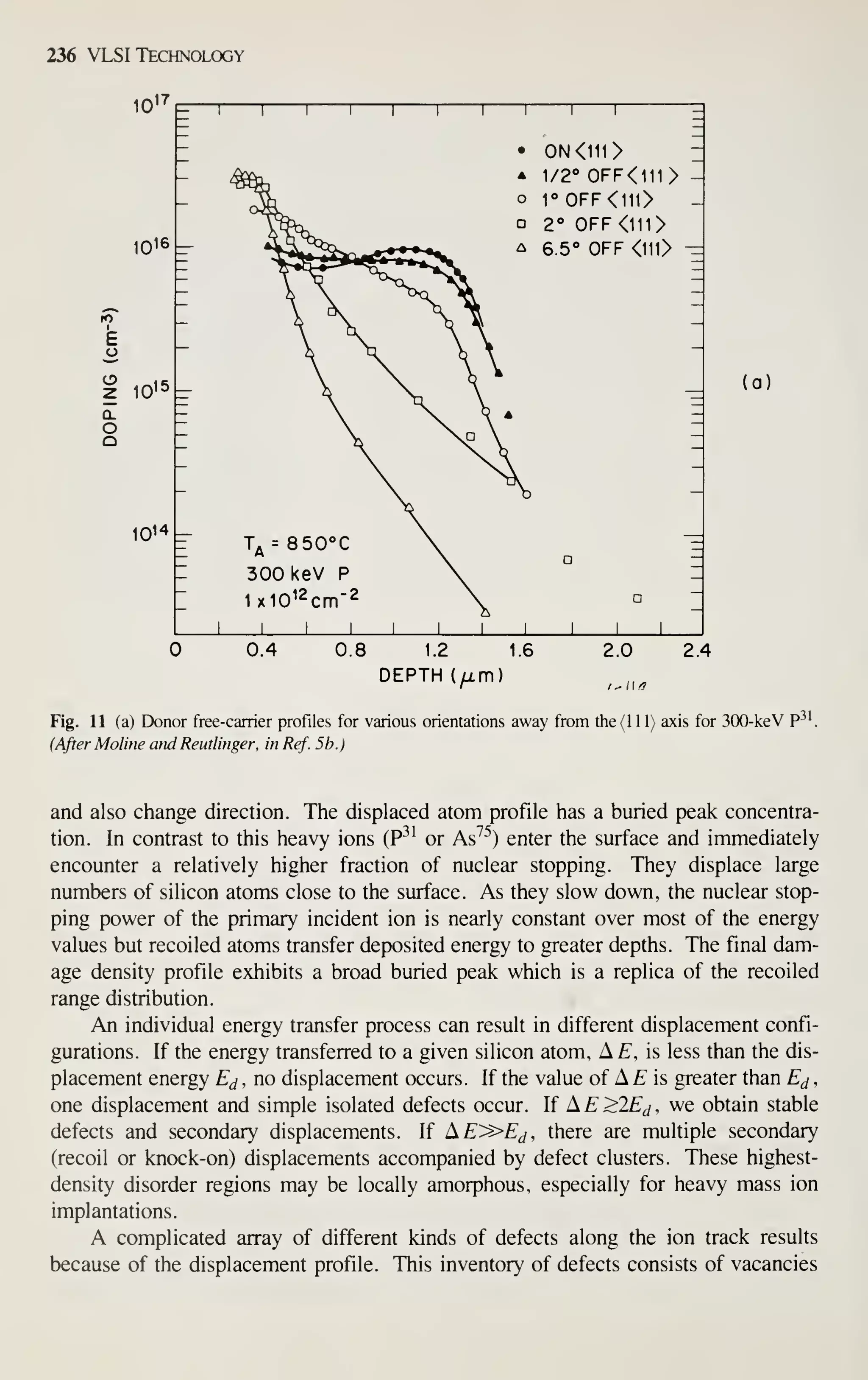
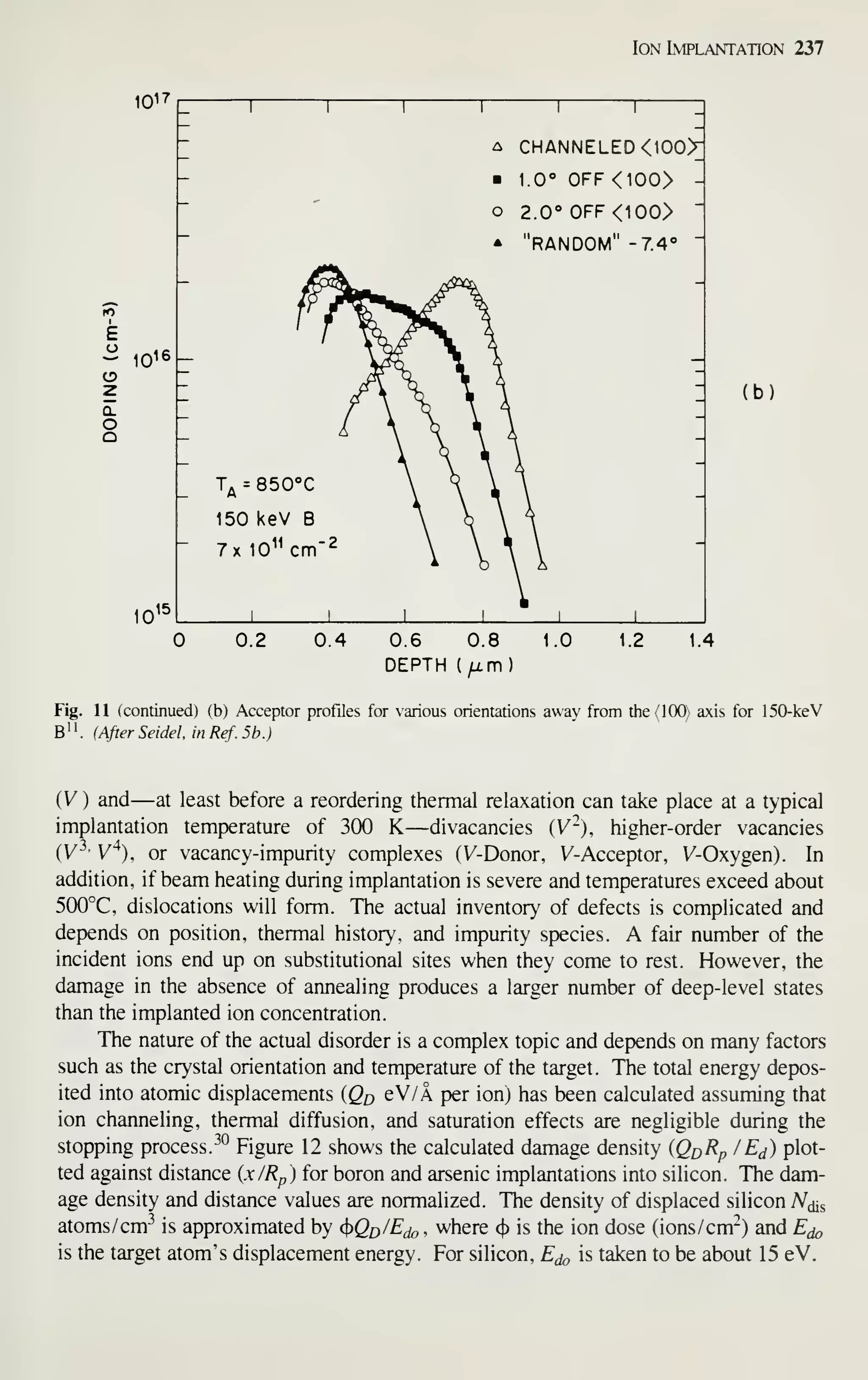
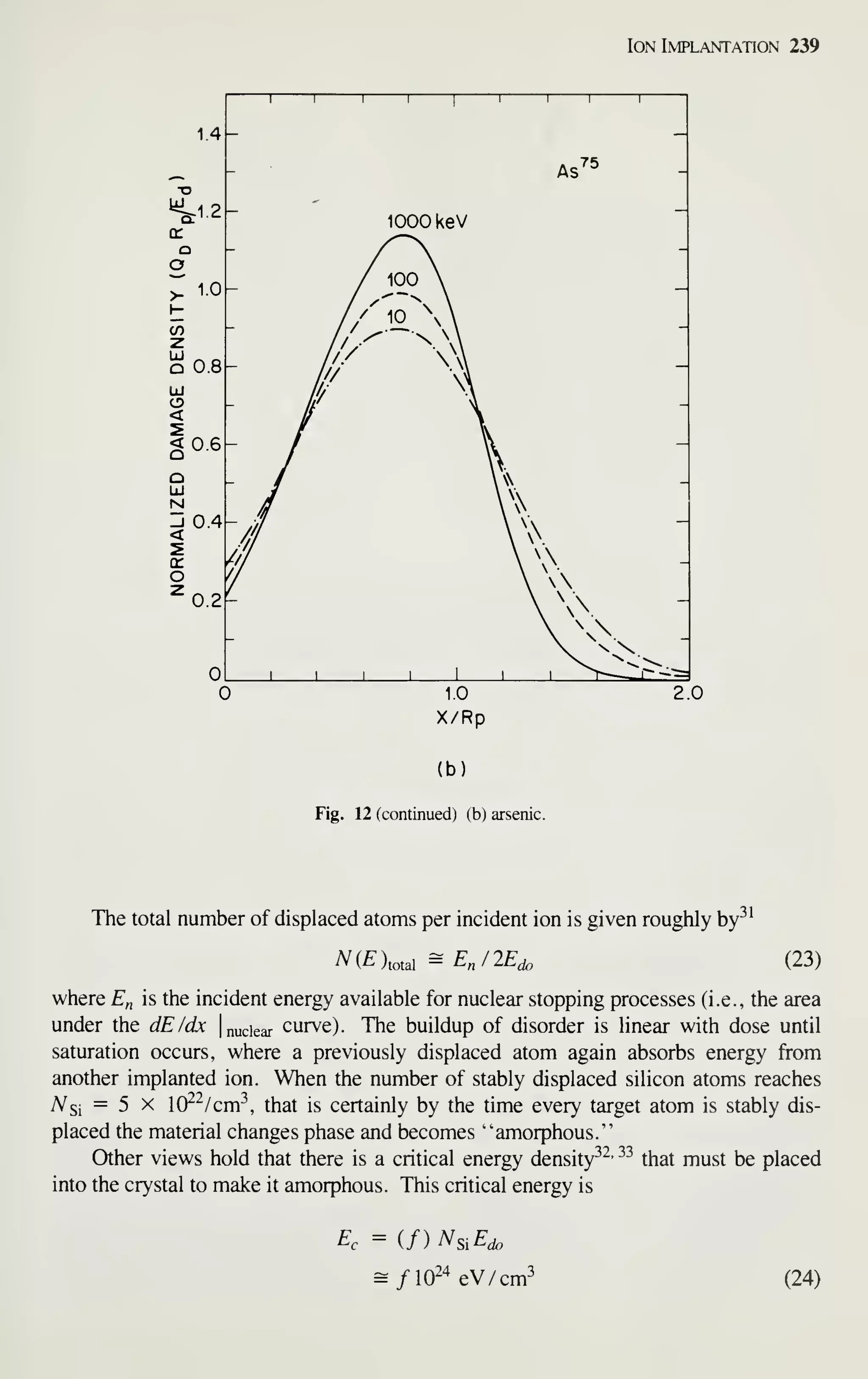
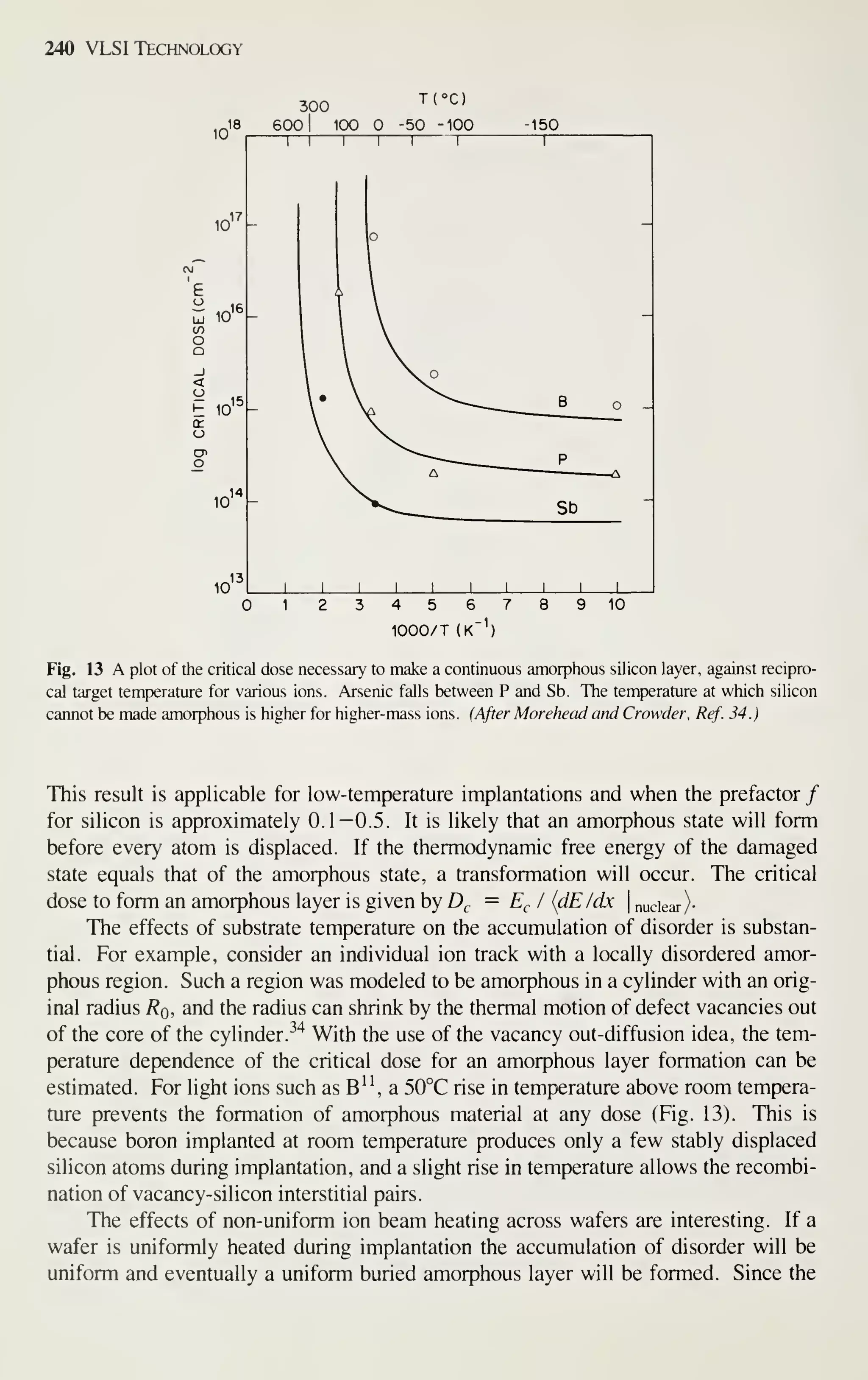
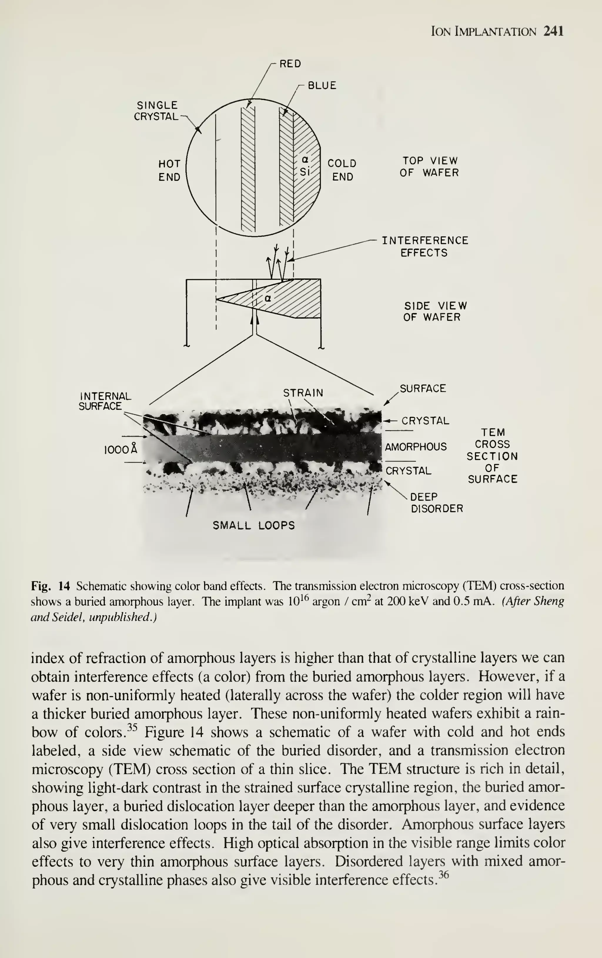
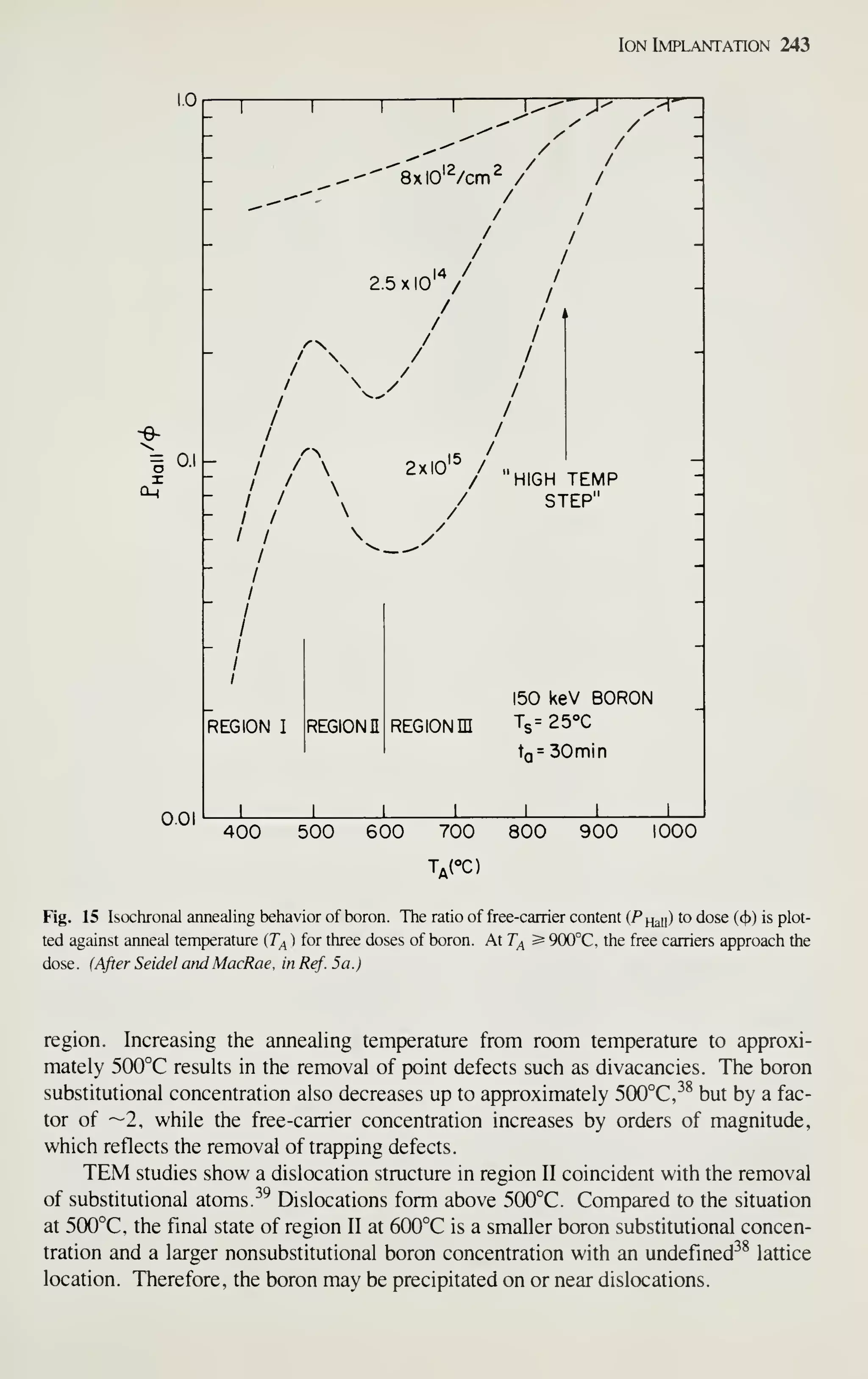
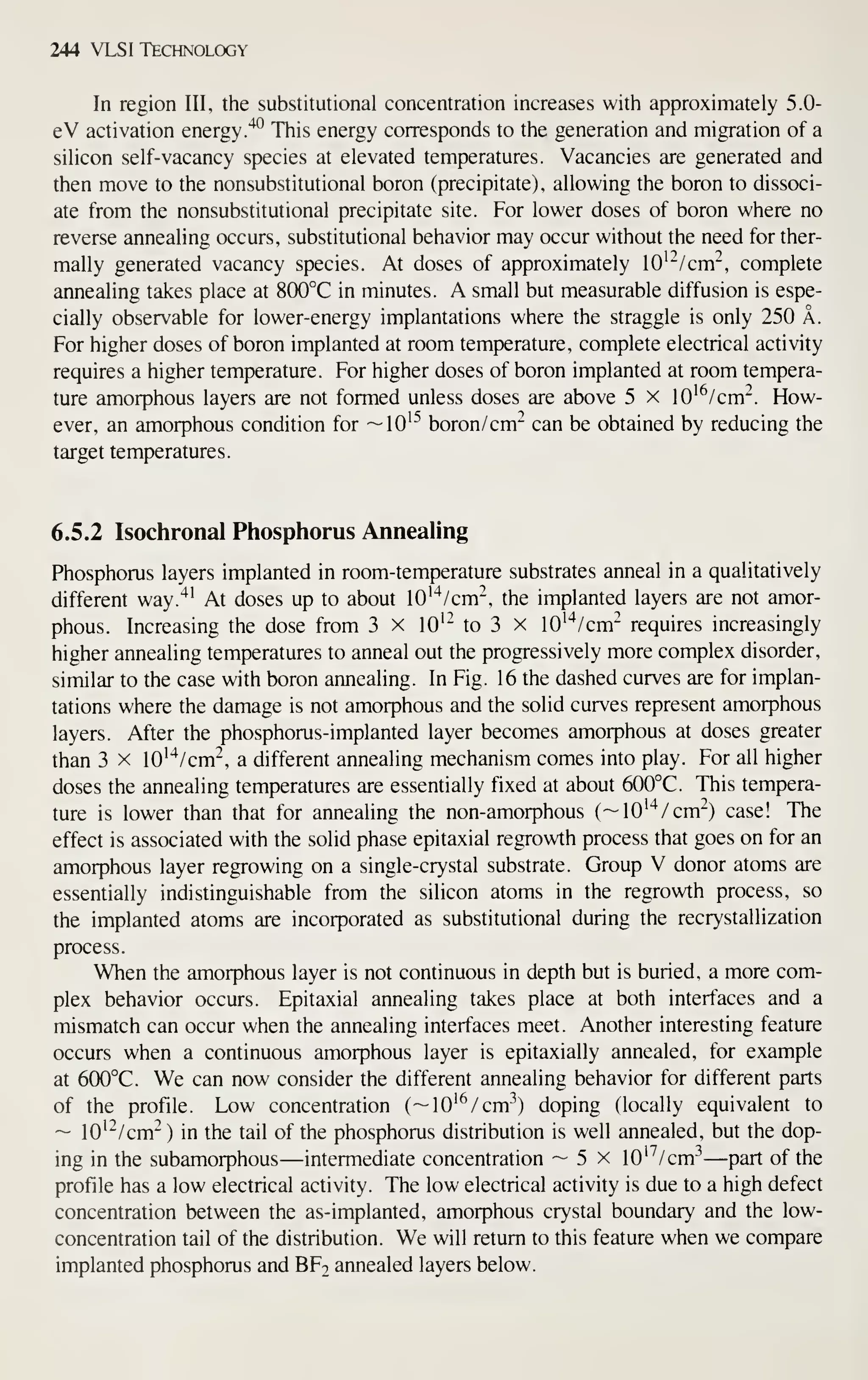
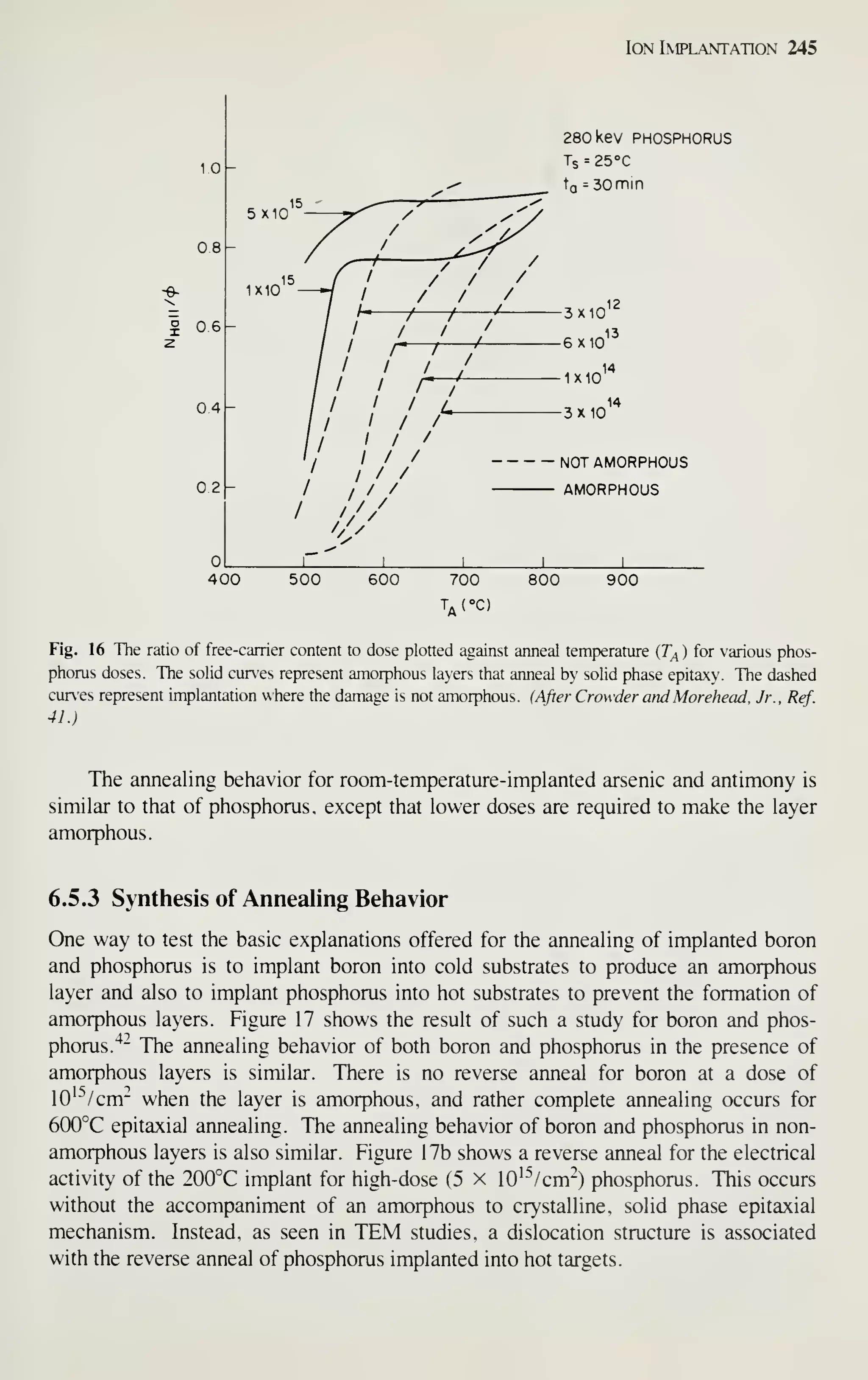
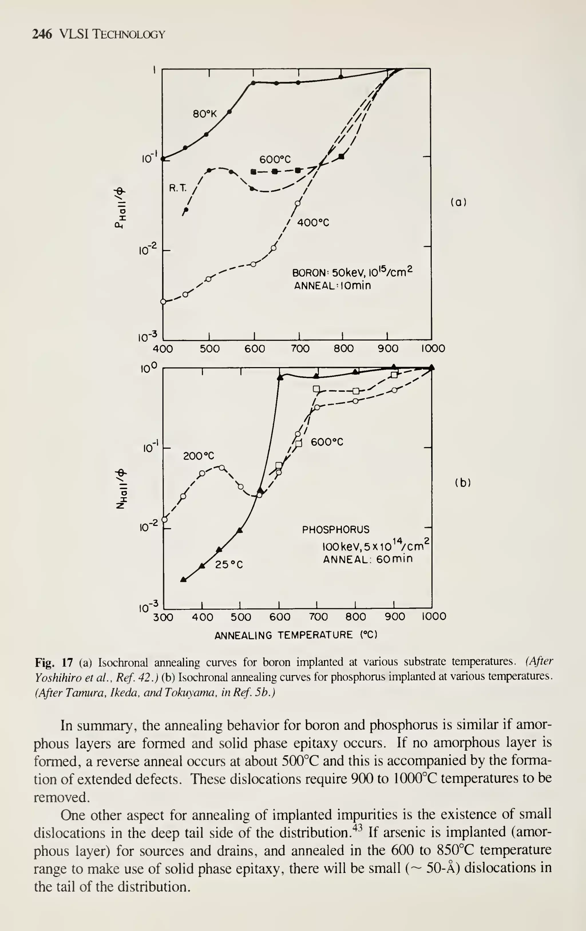
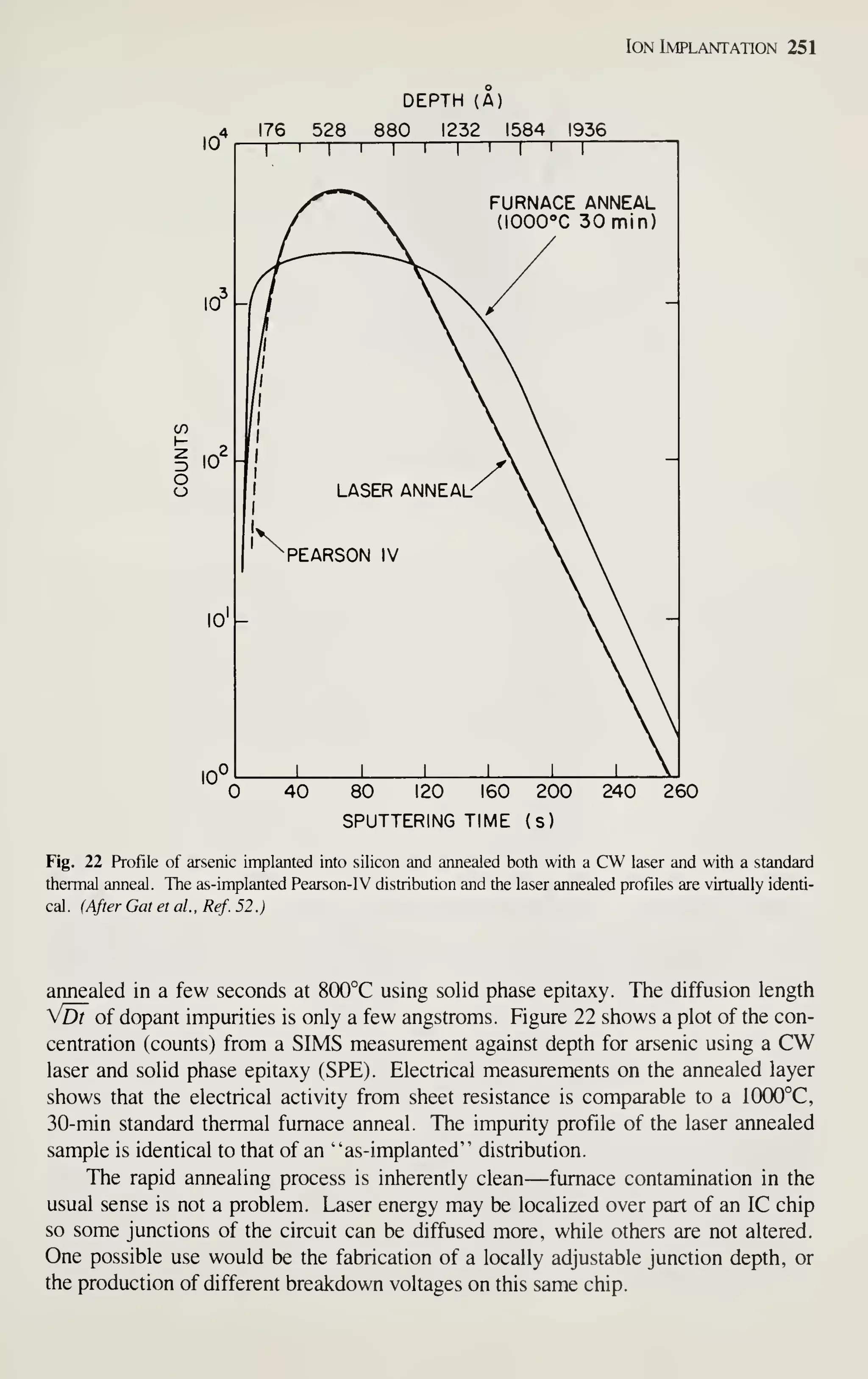
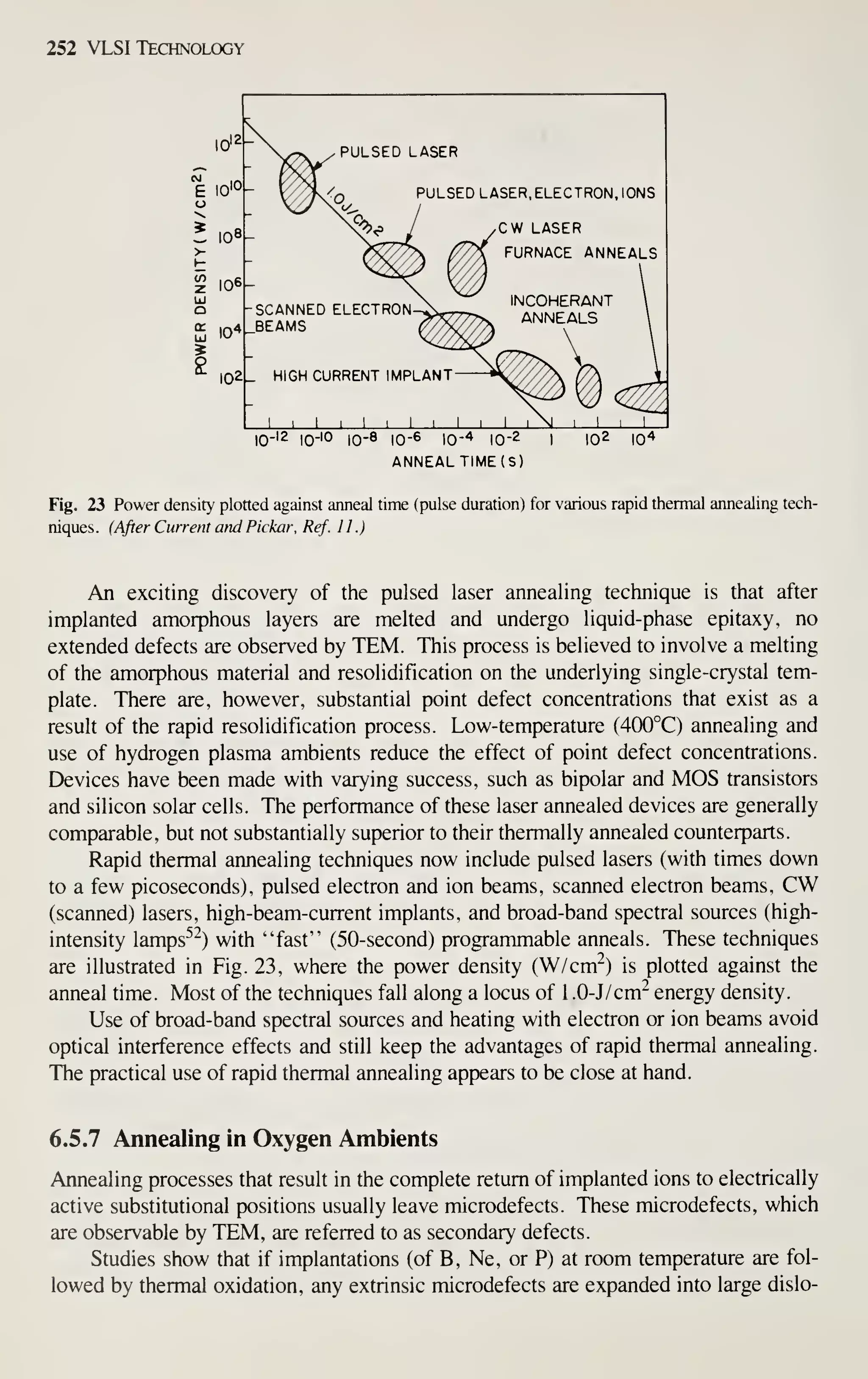
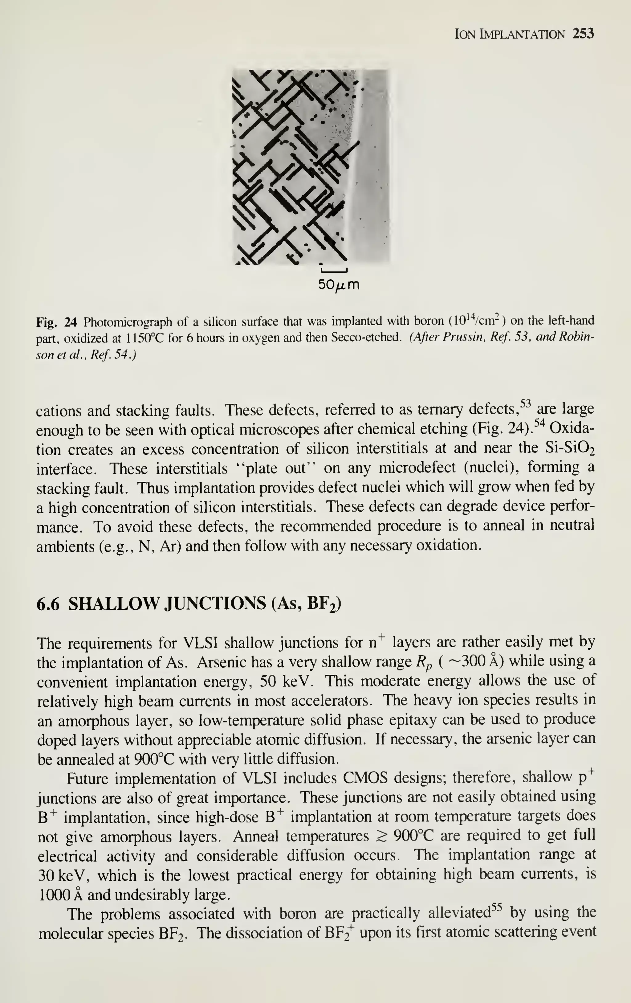
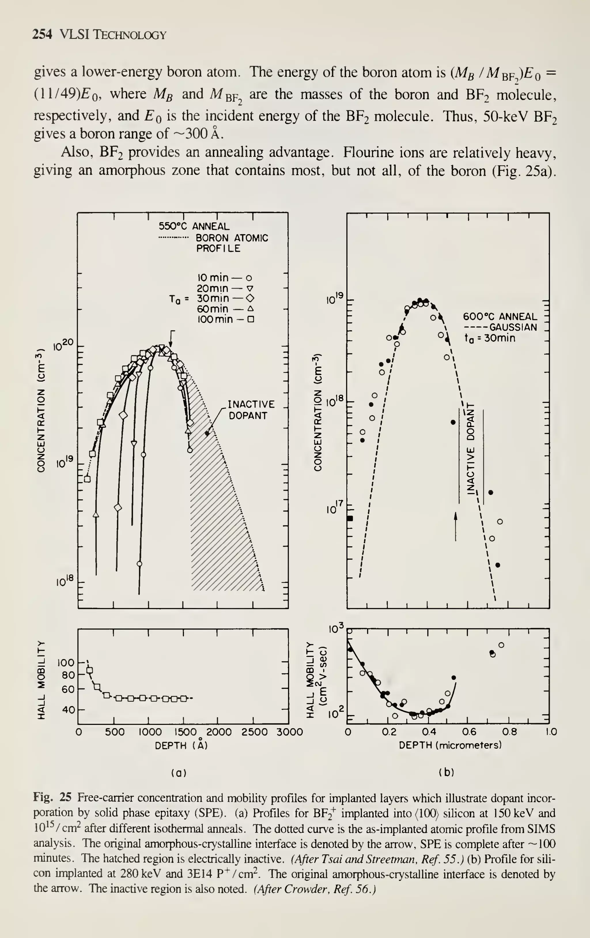
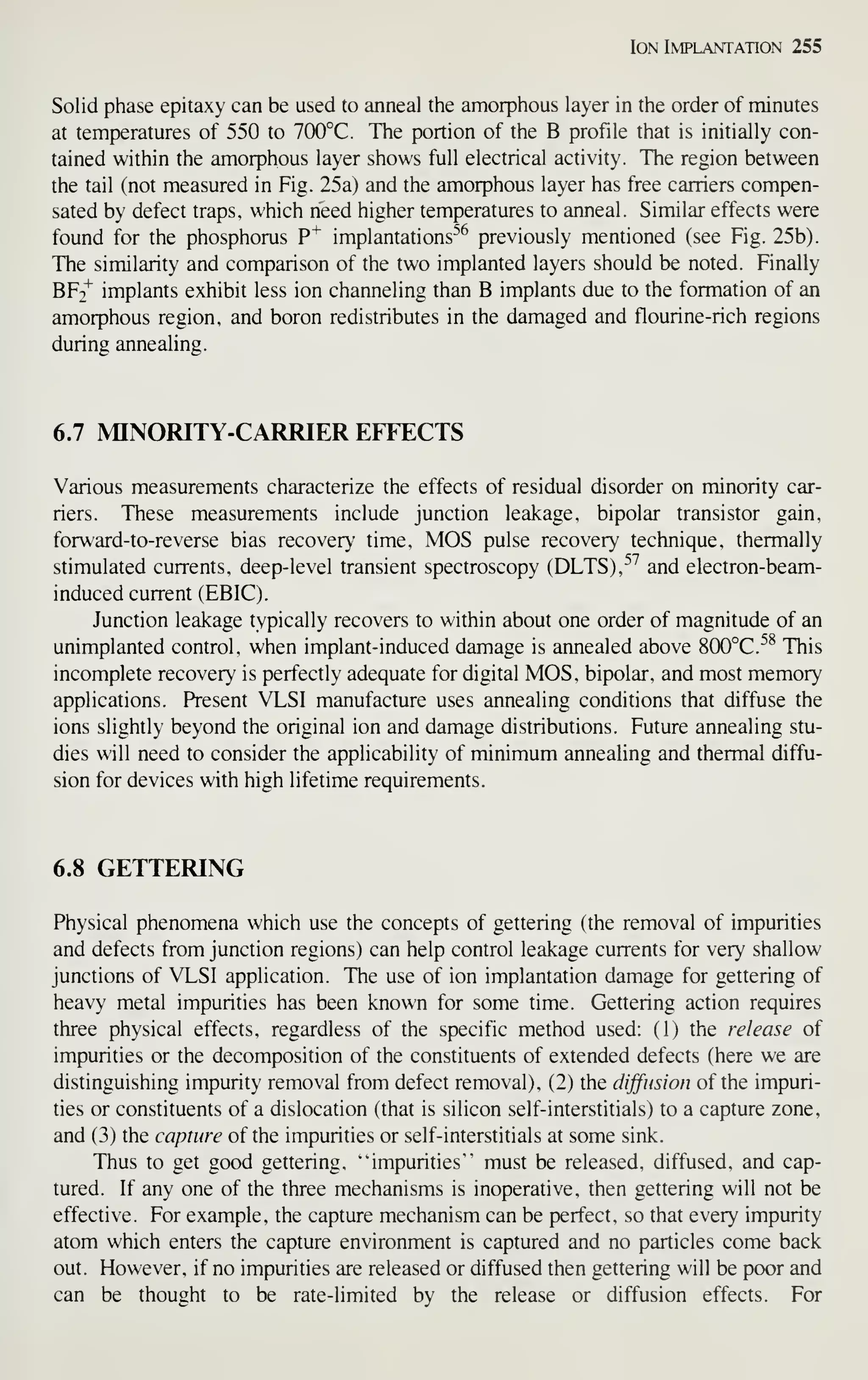
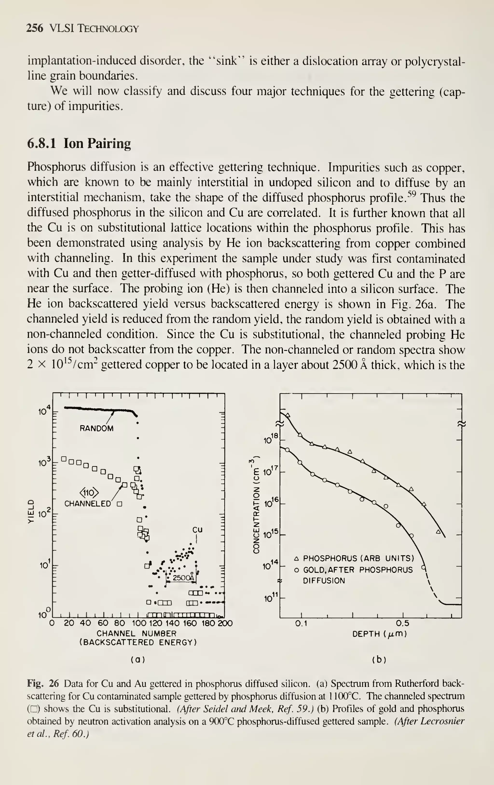
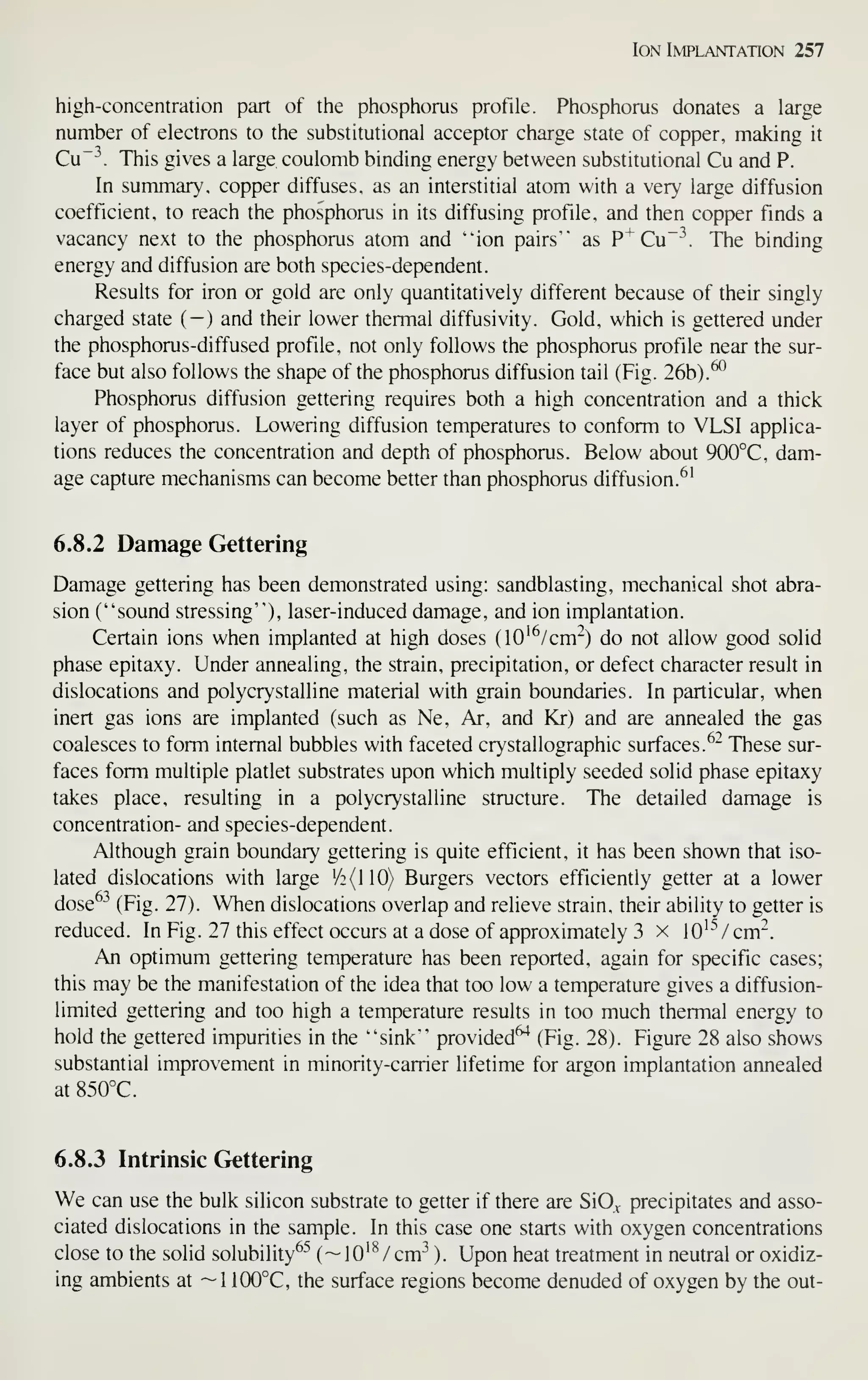
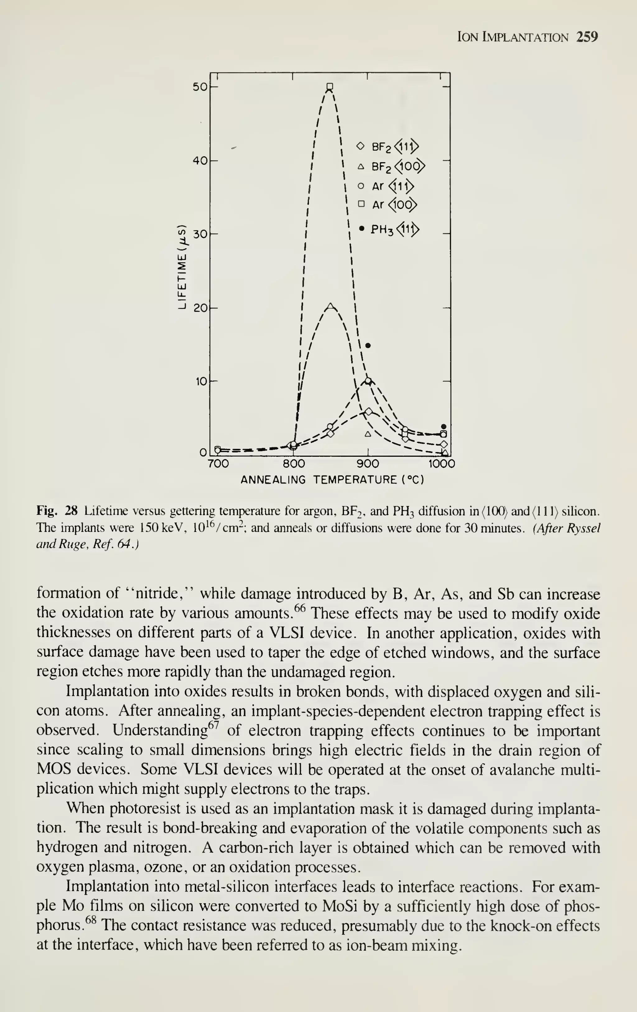
![Ion Implantation 261
lowest possible junctions, it is not at all obvious that low-energy (~3-keV) implanta-
tion will be more useful or practical than thermal diffusion. The past problems of
thermal diffusion (cleanliness, surface oxides, and control of doping concentration)
are not fundamental. The shallowest junctions are probably obtainable from the use
of thermal, and not kinetic, energies. However, implantation, with its obvious advan-
tages, will continue to play a major role in VLSI in the foreseeable future.
REFERENCES
J. Lindhard, M. Scharff. and H. Schiott, "Range Concepts and Heavy Ion Ranges," Mat.-Fys. Med.
Dan. Vid. Selsk 33. No. 14, 1 (1963).
[la] "Proc. International Conference on Atomic Collisions (Chalk River)," Can. J. Phys., 46, 449
(1968).
J. W. Mayer. L. Eriksson, and J. A. Davies, Ion Implantation in Semiconductors. Academic, New
York, 1970. Chapter 4.
J. W. Corbett. "Radiation Damage in Silicon and Germanium," in Ref. 5a. p. 1
.
R. W. Bower and H. G. Dill. Proc. Intemational Electron Device Meeting, 1966, paper 16.6 (unpub-
lished).
F. Eisen and L. Chadderton. Eds.. First International Conference on Ion Implantation. Thousand
Oaks, Gordon and Breach. New York. 1971
.
I. Ruge and J. Graul. Eds.. Second International Conference on Ion Implantation, Garmish,
Springer-Verlag. Berlin, 1972.
B. L. Crowder, Ed., Third International Conference on Ion Implantation, Yorktown Heights, Ple-
num, New York, 1973.
S. Namba. Ed.. Fourth International Conference on Ion Implantation. Osaka, Plenum, New York,
1975.
F. Chemow, J. Borders, and D. Bruce, Eds., Fifth International Conference on Ion Implantation,
Boulder, Plenum, New York, 1976.
J. F. Gibbons, "Ion Implantation in Semiconductors—Part I: Range Distribution Theory and Experi-
ments," Proc. IEEE. 56, 295 (1968).
J. F. Gibbons, "Ion Implantation in Semiconductors—Part U: Damage Production and Annealing,"
Prac/£££. 66, 9(1972).
K. A. Pickar. "Ion Implantation in Silicon—Physics, Processing and Microelectronic Devices," in
R. Wolfe, Ed., Applied Solid State Science. Academic, New York, 1975, Vol. 5.
H. Rupprecht, "New Advances in Semiconductor Implantation," J. Vac. Sci. TechnoL, 15, 1669
(1978).
W. K. Hofker and J. Politick. "Ion Implantation in Semiconductors," Philips Tech. Rev. 39, 1
(1980).
M. I. Current and K. A. Pickar, "Ion Implantation Processing," Electrochemical Society Fall Meet-
ing, Montreal, May 1982, Vol. 82-1, (unpubhshed extended abstracts).
J. Gyulai, Ed., First Internatiotwl Conference on Ion Beam Modification of Materials. Budapest
(1978), Central Res. Inst, for Phys., H-1525 Budapest 1 14, POB49, Hungary, 1978.
R. E. Benenson, E.N.Kaufman, G.L.Miller, and W. W. Scholz, Eds., Second International
Conference on Ion Beam Modification of Materials. Albany (1980), North-Holland, New York,
1981.
M. Wittmer and G. A. Rozgonyi, "Laser Annealing of Semiconductors: Mechanisms and Applica-
tions to Microelectronics," in E. Kaldis, Ed., Current Topics in Materials Science, North-Holland,
New York, 1981.
R. G. Wilson and G. R. Brewer, Ion Beams with Applications to Ion Implantation, Wiley, New
York, 1973; R. G. Wilson and G. R. Brewer, Ion Beams: With Application to Ion Implantation,
Kriegor, Huntington, New York, 1979; and J. F. Ziegler, Ion Particle Accelerators—Applications,
Plenum, New York. 1975.](https://image.slidesharecdn.com/simonm-220913174129-44ec6f82/75/Simon-M-Sze-editor-Very-Large-Scale-Integration-VLSI-Technology-McGraw-Hill-Inc-US-1983-pdf-281-2048.jpg)
![Ion Implantation 263
[43] H. Foell. T. Y. Tan. and W. Krakow, "Undissociated Dislocations and Intermediate Defects," in
J. Narayan and T. Y. Tan, Eds., Defects in Semiconductors. North-Holland, New York, 1981.
Vol. 2,'p. 173.
[44] J. M. Fairfield and B. J. Masters, '"Self- Diffusion in Intrinsic and Extrinsic Silicon,'" J. Appl. Phys.,
38.3148(1967).
[45] A. Chu and J. F. Gibbons, ""A Theoretical Approach to the Calculation of Impurity' Profiles for
Annealed Ion Implanted B in Si," in Ref. 5e. p. 71 1.
[46] L. Csepregi, J. W. Mayer, and T. W. Sigmon, Appl. Phys. Lett.. 29. 92 (1976); and S. T. Picreaux.
"Ion Channeling Analysis of Disorder." in J. Narayan and T. Y. Tan. Eds.. Defects in Semiconduc-
tors. North-Holland. New York. 1981. Vol. 2. p. 135.
[47] L. Csepregi. W. K. Chu. H. Muellor. and J. W. Mayer, "Influence of Thermal Histor' on the Resi-
dual Disorder in Implanted- 1 1 1 Silicon." Radiat Eff.. 28. 277 ( 1976).
[48] E. I. Alessandrini. W. K. Chu. and M. R. Poponiak. "TEM Study of the Two Step Annealing of
Arsenic-Implanted. 100) Silicon." J. Vac. Sci. TechnoL. 16, 342 (1979).
[49] T. E. Seidel and A. U. MacRae. "Some Prop)erties of Ion Implanted Boron in Silicon." Trans.
Metall. Sac. AIME. 245, 491 ( 1969).
[50] E. C. Douglas and A. G. F. Dingwall. "Ion Implantation for Threshold Control in COSMOS Cir-
cuits," IEEE Tram. Electron Devices. ED-21. 324 ( 1974).
[51] B. R. Appleton and G. K. Aller. Eds.. Laser arid Electron Beam Interactions with Solids. North-
Holland. New York. 1982.
[52] A. Gat et al.. "Physical and Electrical Properties of Laser-Annealed Ion Implanted Silicon." Appl.
Phys. Lett.. 32. 276 (1978). and A. Gat. "Heat Pulse Annealing of Arsenic-Implanted Silicon with a
CW Arc Lamp." IEEE Electron Device Lett.. EDL-2. p. 85 (1981). and T. O. Sedgwick. "Short
Time Annealing," in C. J. Dell'Oca and W. M. BuUis, Eds.. VLSI Science and Technology,
Vol. 82-7. The ElecL-ochemical Soc.. Pennington. NJ 1982 p. 130.
[53] S. Prussin. "Role of Sequential Annealing. Oxidation and Diffusion Upon Defect Generation in Ion-
Implanted Silicon Surfaces." y. Appl. Phys.. 45. 1635 (1974).
[54] McD. Robinson. G. A. Rozgonyi. T. E. Seidel. and M. H. Read, "Orientation and Implantation
Effects on Stacking Faults During Silicon Buried Layer Processing." J. Electrochem. Soc, 128. 926
(1981).
[55] M. Y. Tsai and B. G. Streetman. "Recrystallization of Implanted Amorphous Silicon Layers, I.
Electrical Properties of Silicon hnplanted with BF;* or Si* + B*." J. Appl. Phys.. 50, 183 ( 1979).
[56] B. L. Crowder, "Influence of Amorphous Phase on Ion Distributions and Annealing Behavior of
Group III and Group V Ions Implanted into Silicon," 7. Electrochem. Soc. 118, 943 ( 1971).
[57] L. C. Kimmerling. "Defect Characterization by Junction Spectroscopy." in J. Narayan and
T. Y. Tan. Eds.. Defects in Semiconductors. North-Holland. New York, 1981, Vol. 2, p. 85.
[58] K. A. Pickar and J. V. Dalton. "Lifetime Effects in Ion Implanted Silicon." in Ref. 5a, p. 125.
[59] T. E. Seidel and R. L. Meek. "Ion Implantation Gettering and Phosphorus Diffusion Gettering of Cu
and Au in Silicon." in Ref. 5c. p. 305.
[60] D. Lecrosnier. J. Paugam. F. Richou. G. Pelous. and F. Beniere. "Influence of Phosphorus-Induced
Point Defects on a Gold-Gettering Mechanism in Silicon." J. Appl. Phys.. 51, 1036 (1980).
[61] T. E. Seidel. R. L. Meek, and A. G. CuUis. "Direct Comparison of Ion Damage Gettering and
Phosphorus-Diffusion Gettering of Au in Si." J. Appl. Phys.. 46. 600 ( 1975).
[62] A. G. Culhs. T. E. Seidel. and R. L. Meek. "Comparative Study of Annealed Neon. Argon, and
Kr>'pton Ion Implantation Damage in Silicon," 7. Appl. Phys.. 49, 5188 ( 1978).
[63] H. J. Geipel and W. K. Tice. "Reduction of Leakage by Implantation Gettering in VLSI Circuit,"
IBM J. Res. Dew. 24. 310 ( 1980).
[64] H. Ryssel and 1. Ruge. "New Applications of Ion Implantation in Semiconductor Technology," in
W. A. Kaiser and W. E. Proebster, Eds., Electronics to Microelectronics, North-Holland, New
York. 1980, p. 63.
[65] T. Y. Tan, E. E. Gardner, and W. K. Tice, "Intrinsic Gettering by Oxide Precipitate Induced Dislo-
cations in Czochralski Si." Appl. Phys. Lett., 30. 175 (1977).
[65a] H. Shiraki, "Stacking Fault Generation Suppression and Grown-In Defect Elimination in Dislocation
Free Sihcon Wafers by HCl Oxidation." Jap. Jour. Appl. Phys. 15. 1 ( 1976).
[66] W. J. M. J. Josquin, "The Oxidation Characteristics of Nitrogen Implanted Silicon," in Ref. 12, p.](https://image.slidesharecdn.com/simonm-220913174129-44ec6f82/75/Simon-M-Sze-editor-Very-Large-Scale-Integration-VLSI-Technology-McGraw-Hill-Inc-US-1983-pdf-283-2048.jpg)
![264 VLSI Technology
1433; and J. F. Gotzlich, et al., "Dopant Dependence of the Oxidation Rate of Ion Implanted Sili-
con," in Ref. 12, p. 1419.
[67] R. F. DeKeersmaecher and D. J. DiMaria. "Electron Trapping and Detrapping Characteristics of
Arsenic-Implanted SiOo Layers," J. Appl. Phys.. 51, 1085 ( 1980).
[68] S. W. Chiang, T. P. Chow, R. F. Reihl, and K. L. Wang, "The Effect of Phosphorus Ion Implanta-
tions on Molybdenum/Silicon Contacts," 7. Appl. Phys., 52, 4027 ( 1981).
[69] M. Wittmer and T. E. Seidel, "The Redistribution of Implanted Doponts After Metal-Silicides For-
mation," J. Appl. Phys.. 49, 5826 (1978).
[70] J. M. Shannon, "Shallow Implanted Layers in Advanced Silicon Devices," in Ref. 13, p. 545.
Additional reading
See J. L. Stone and J. C. Plunkett, "Ion Implantation Processes in Silicon" (Chapter 2) and H. Maes,
W. Vandervorst, and R. van Overstraeten. "Impurity Profile of Implanted Ions in Silicon" (Chapter 8), in
F. F. Y. Wang, Ed., Material Processing Theory arid Practices. Vol. 2: Impurity Doping Processes in Sili-
con, North-Holland, New York, 1981.
PROBLEMS
1 A 10-|xA ion beam has a 10° half-angle divergence as it passes through a square aperture (8 cm x 8 cm),
placed 6 cm away from the target. Using a current meter, how much time is needed to implant lO'^
atoms/cm^ for (a) a singly ionized, monatomic species, (b) a triply ionized diatomic species? Using a
charge integrator (measures It) calibrated for a singly ionized monatomic species, (c) what dose should be
"set" to obtain lO'^ atom/cm" for the triply ionized diatomic species?
2 The drift-space vacuum between a mass-separation magnet and the target is approximately 10"^ Torr.
Consider the possibility of a neutralizing charge exchange reaction
1+ + N2 ^ I^ + N2+
with a cross section of 10"^ cnt/atom. What percent of the ions are charge exchanged in a distance of 1 m?
Take the (probability) fraction of unreacted particles to be exp ( -.x I K) where X is the mean free path.
3 (a) Identify the three minor species peaks in Fig. 3. Use the relative magnetic-field values of 7.7, 9.9,
and 13.3. F2^ is atB = 8.9, and As+ atfl = 12.5. Make a list of the ion species.
(b) Can AsF4"^"'' and F/ be resolved from As"*"?
(c) Discuss beam purity.
(d) Discuss solutions that would improve beam purity.
4 An existing accelerator has a lO-fi, A beam current with a 1-cm- area and deflection plates (x,v scan) that
are separated by 2 cm and have a 2-kV saw-tooth sweep voltage. Consider 10-keV As^'' as the ion of
interest. The ion beam's charge density can cause a drop in the sweeping electric field.
(aj What is the magnitude of the drop in the sweeping electric field at the center of the beam?
(b) Should this machine be retrofitted with a 1 .0-mA beam source? Assume no geometry changes.
(c) Discuss alternatives for scanning high beam currents.
5 (a) Using Fig. 7, approximate {dE Idx ) total as a constant and calculate the range R. Compare at 30 and
300 keV for As, P, and B with R^ values from Fig. 8.
(b) Calculate the sheet resistance for 30-keV lO'^ As^'' atoms/cm- and lO'^ B¥f atoms/cm-. Assume
a fuUy active Gaussian nondiffused dopant profile. The profile can be approximated by equally spaced
strips of constant doping and mobility.](https://image.slidesharecdn.com/simonm-220913174129-44ec6f82/75/Simon-M-Sze-editor-Very-Large-Scale-Integration-VLSI-Technology-McGraw-Hill-Inc-US-1983-pdf-284-2048.jpg)

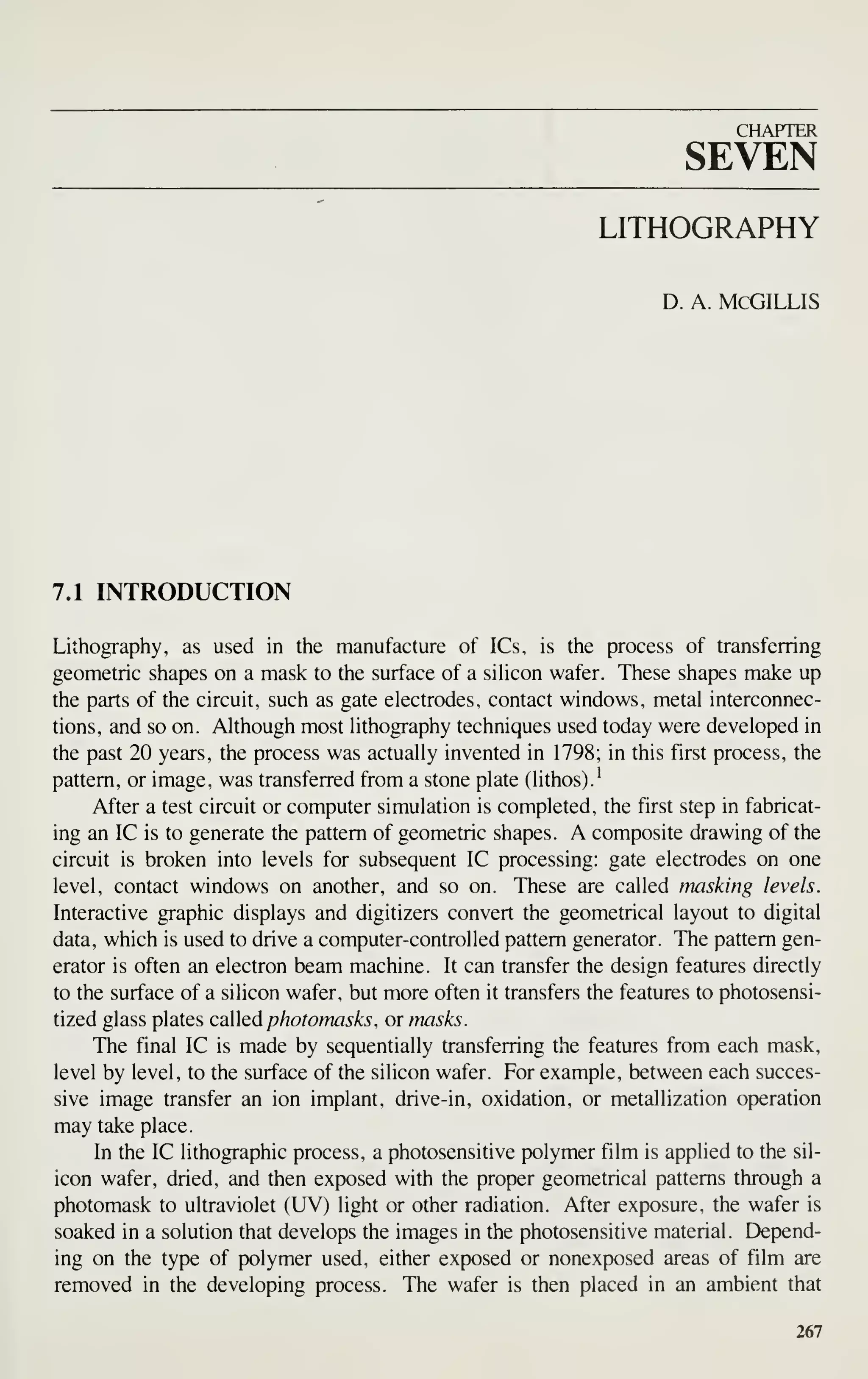
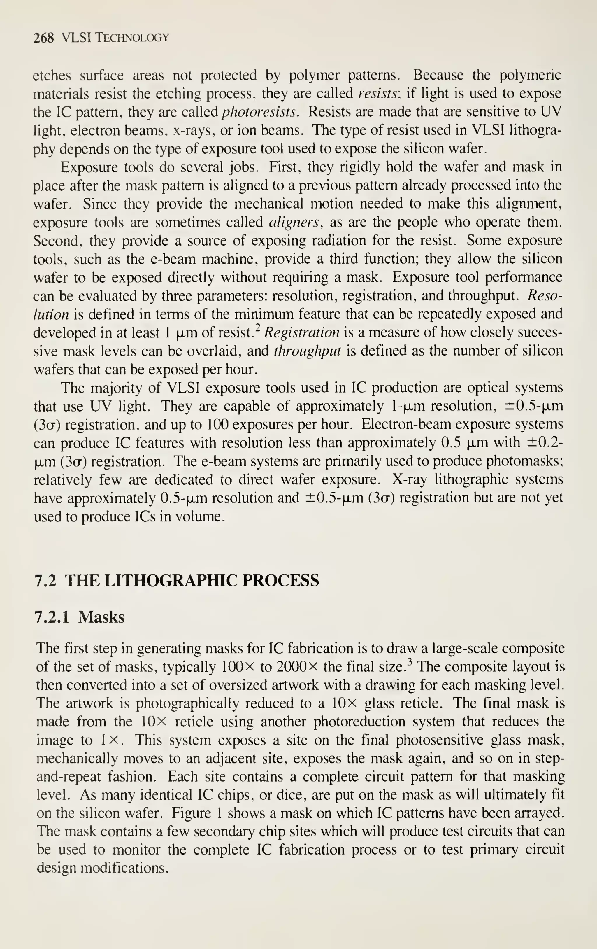
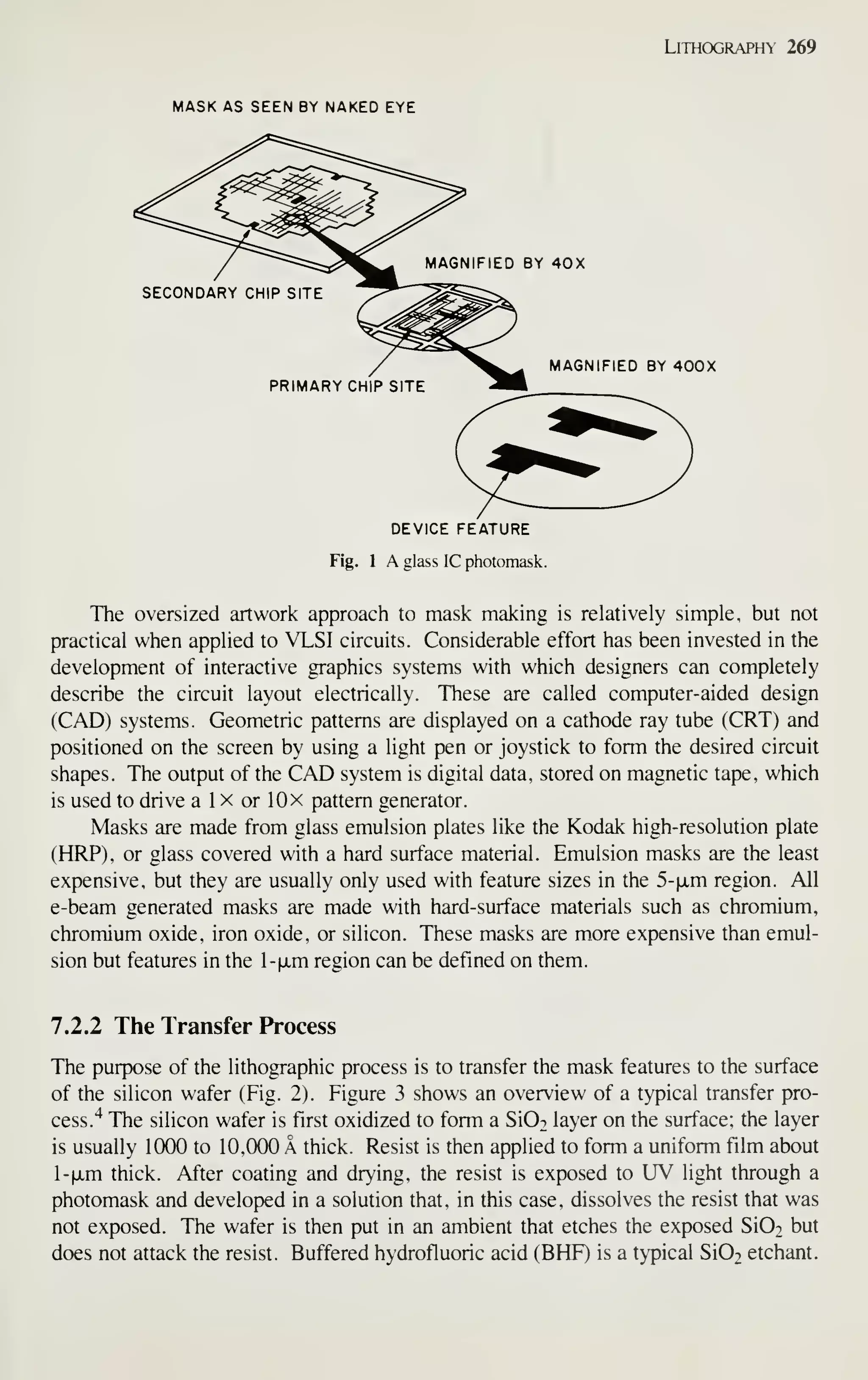
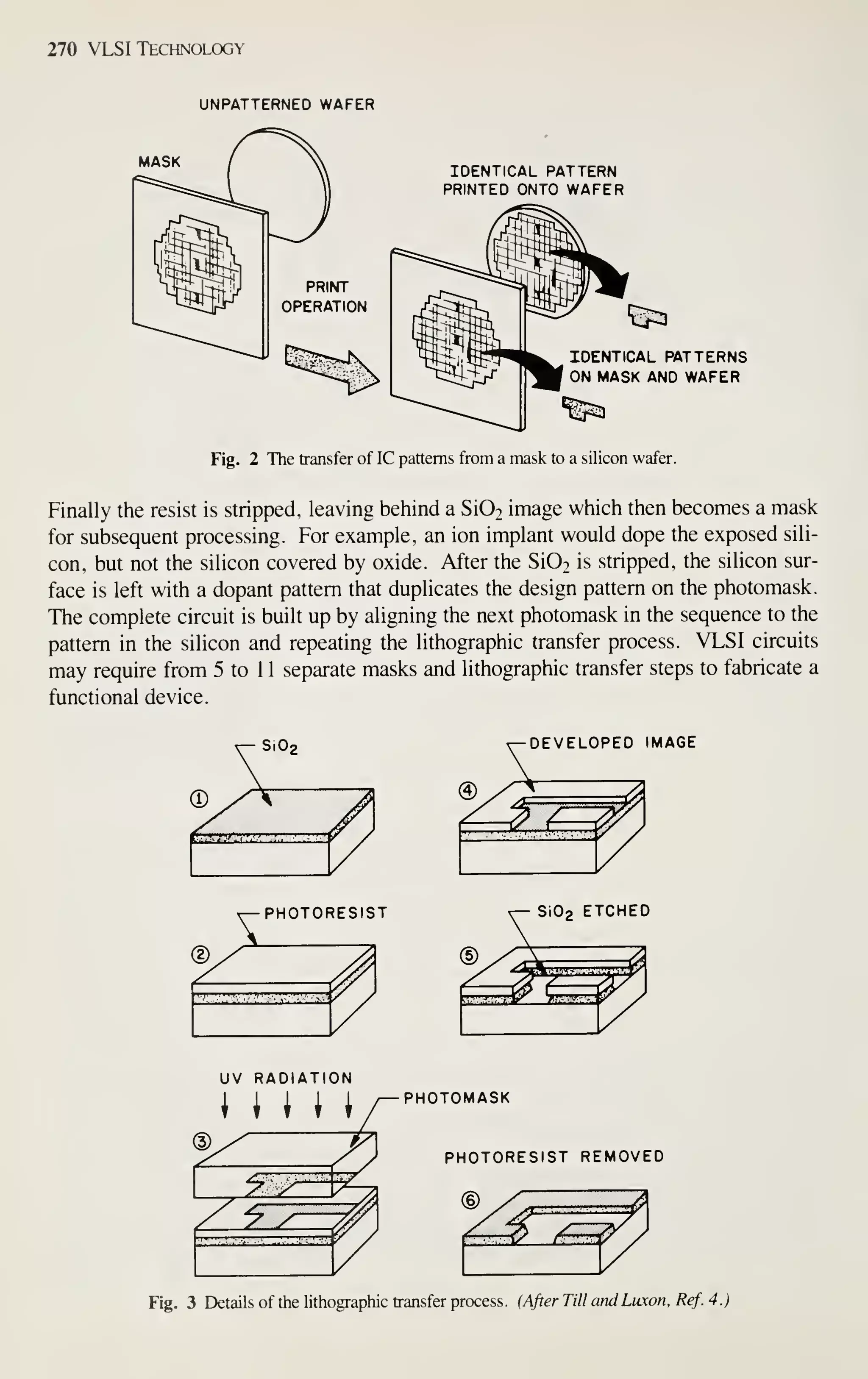
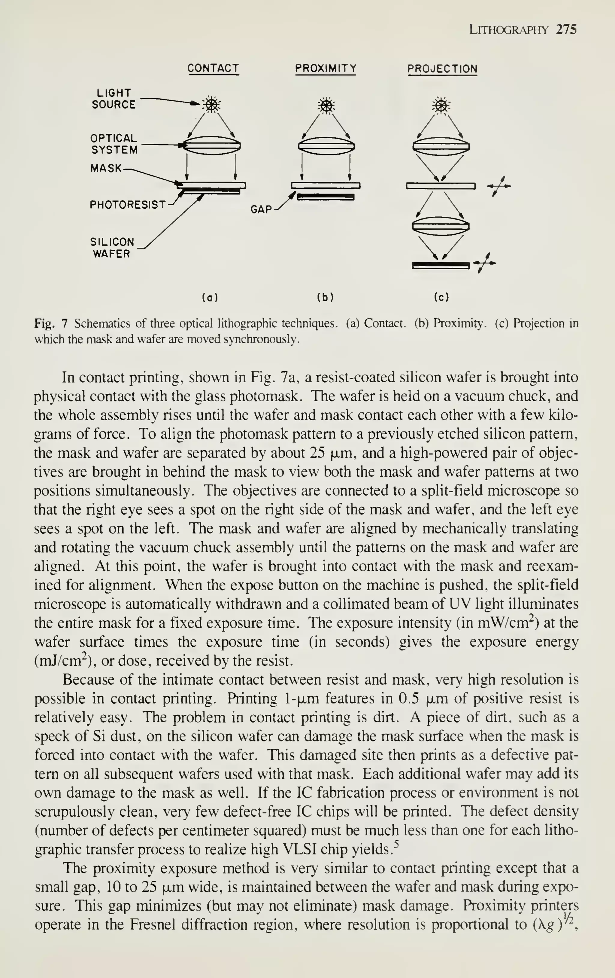
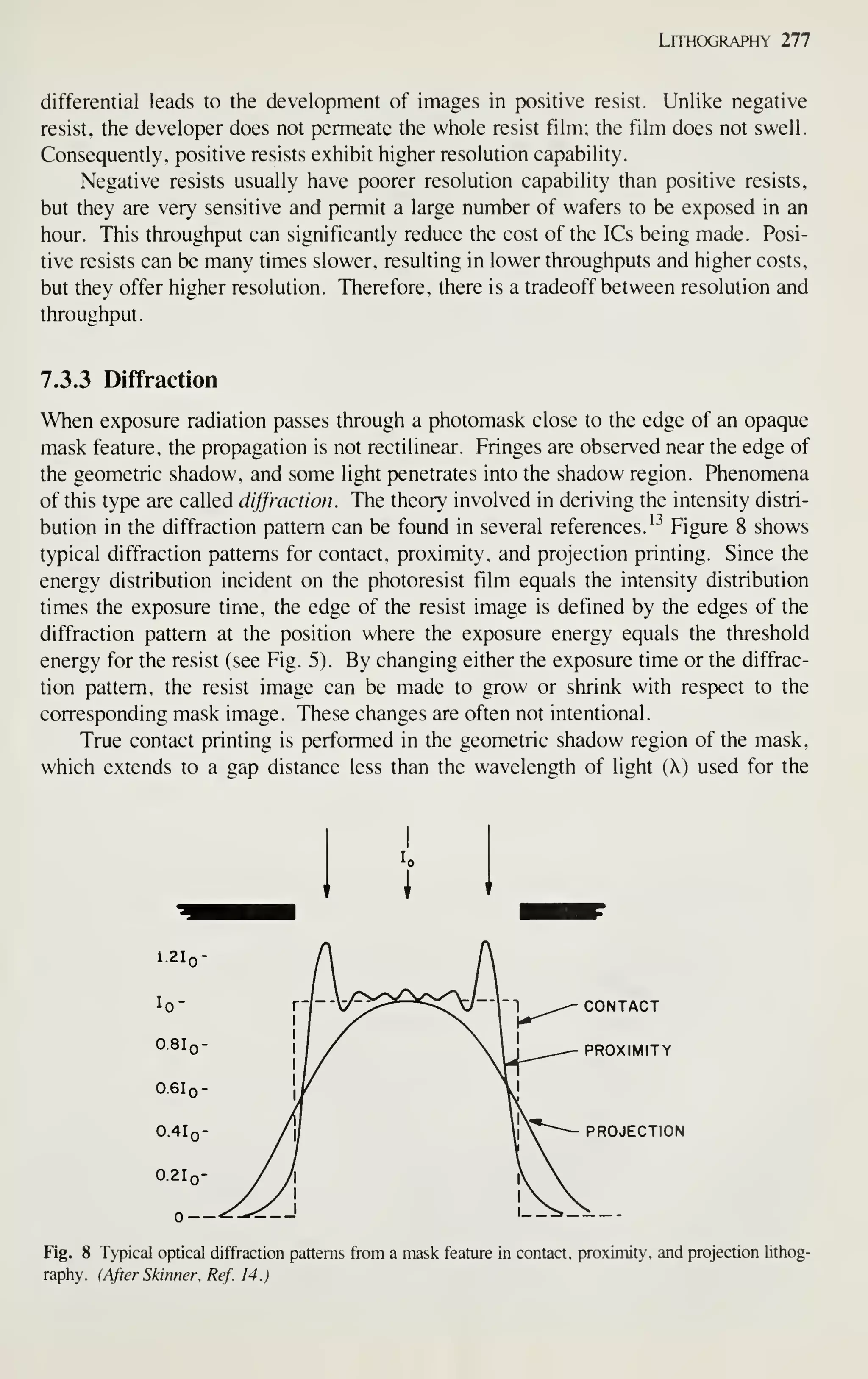
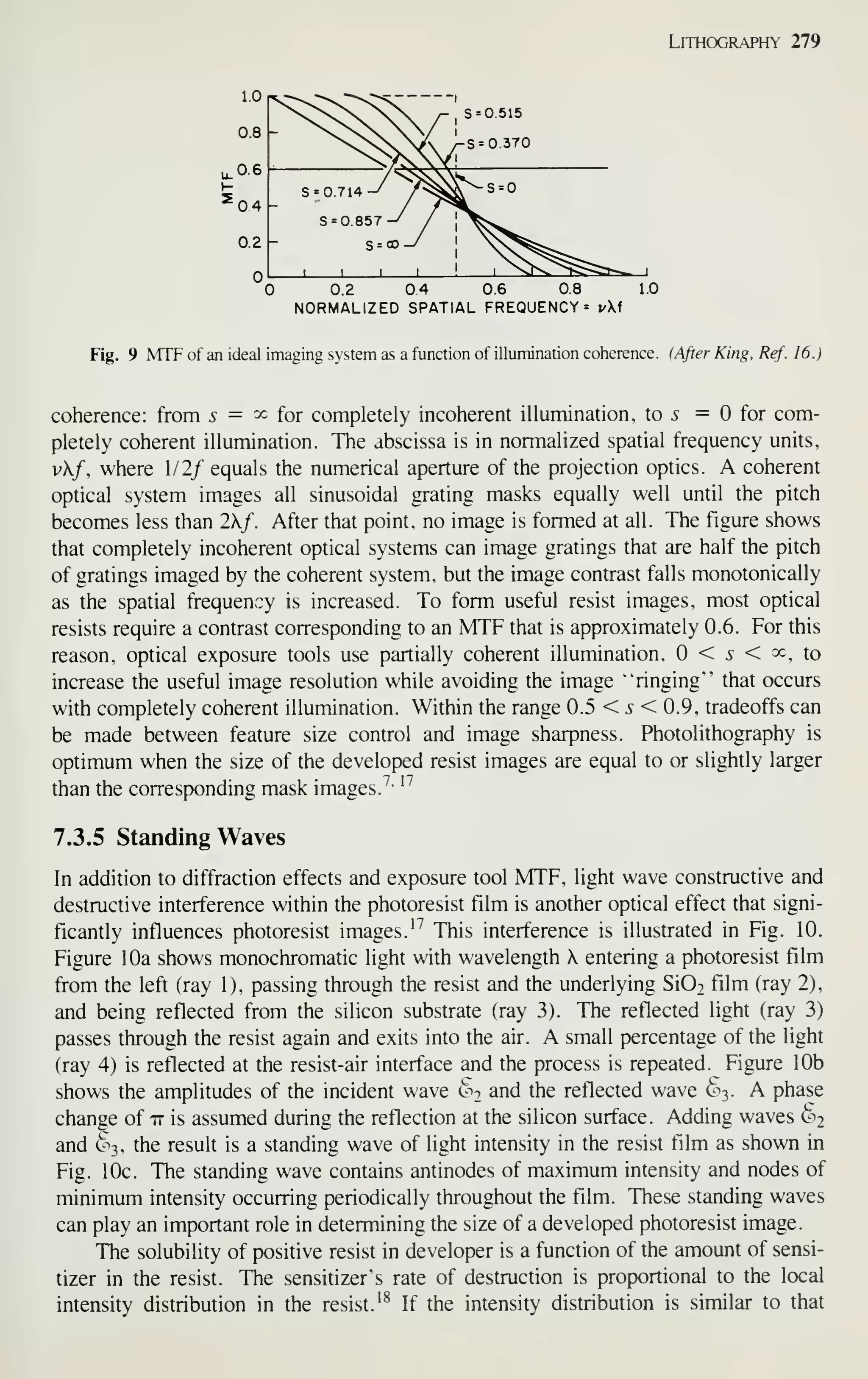
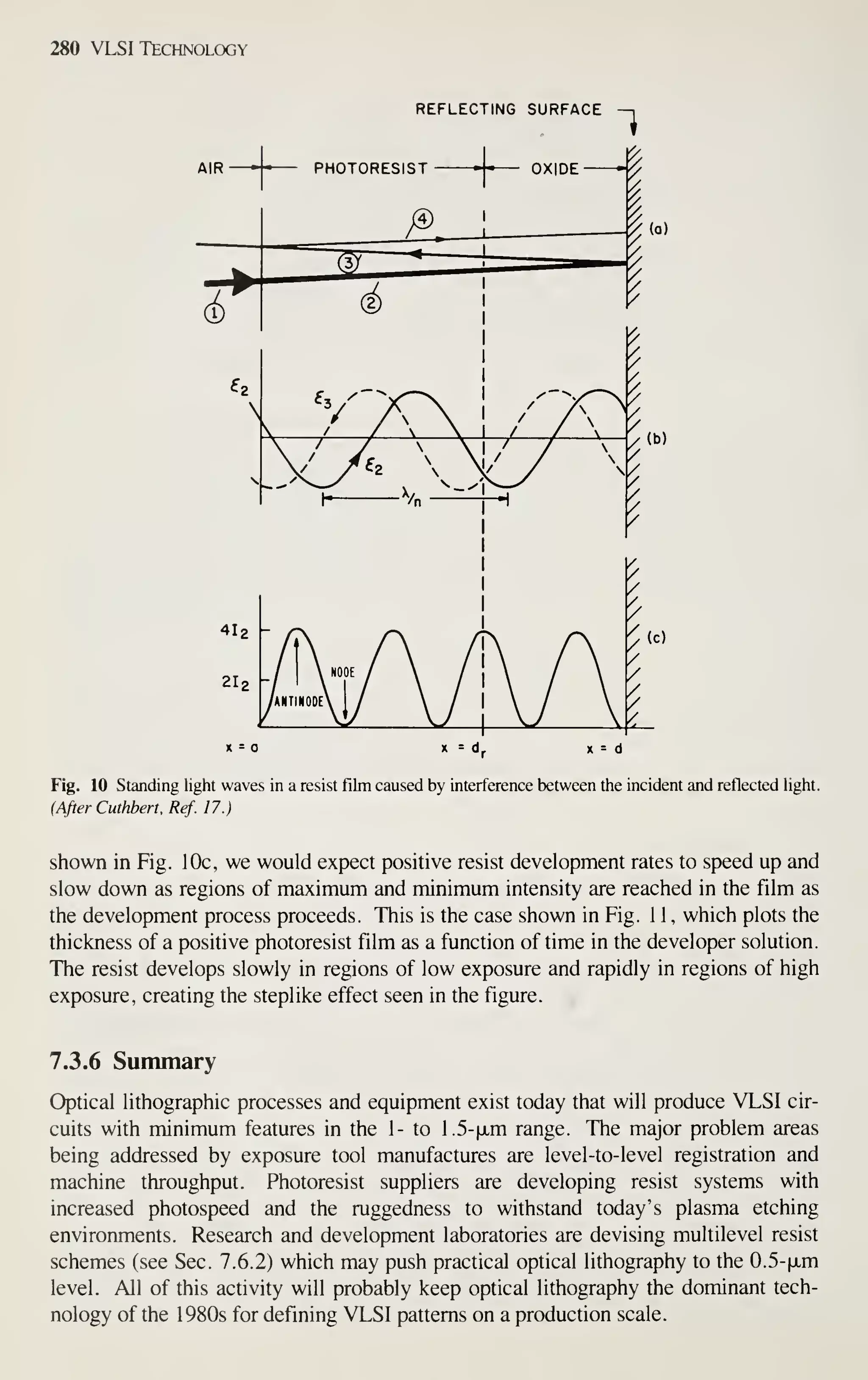
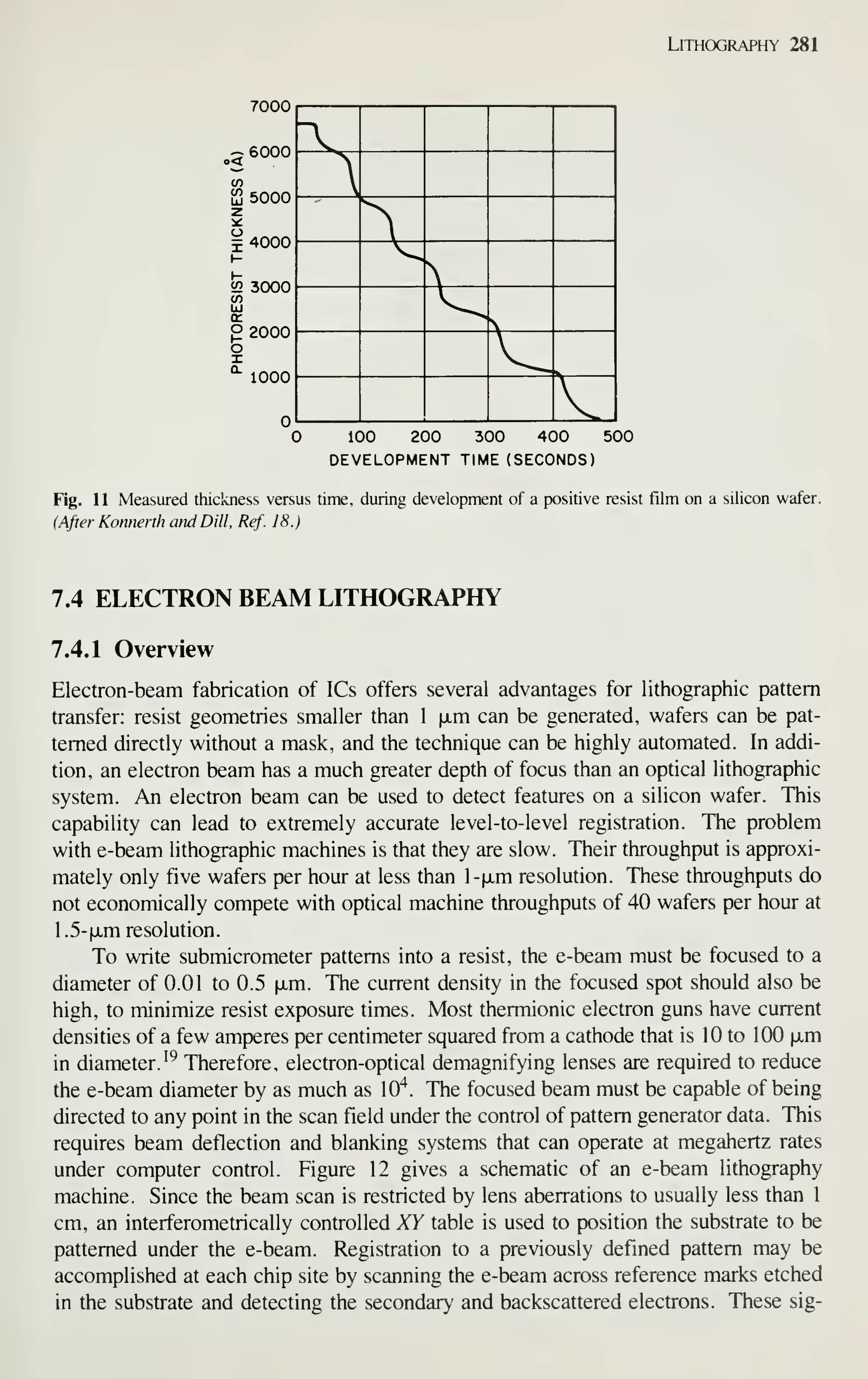
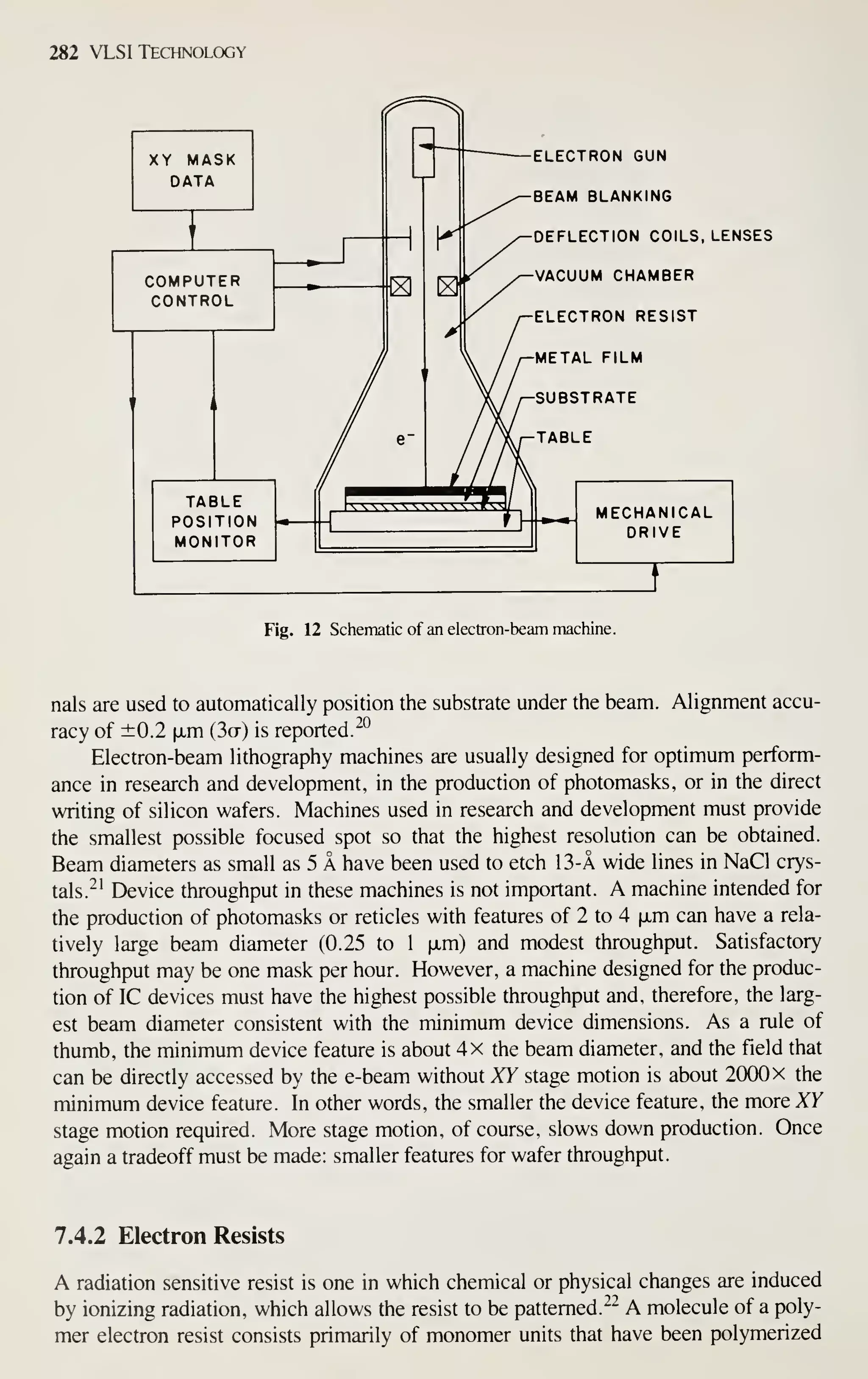
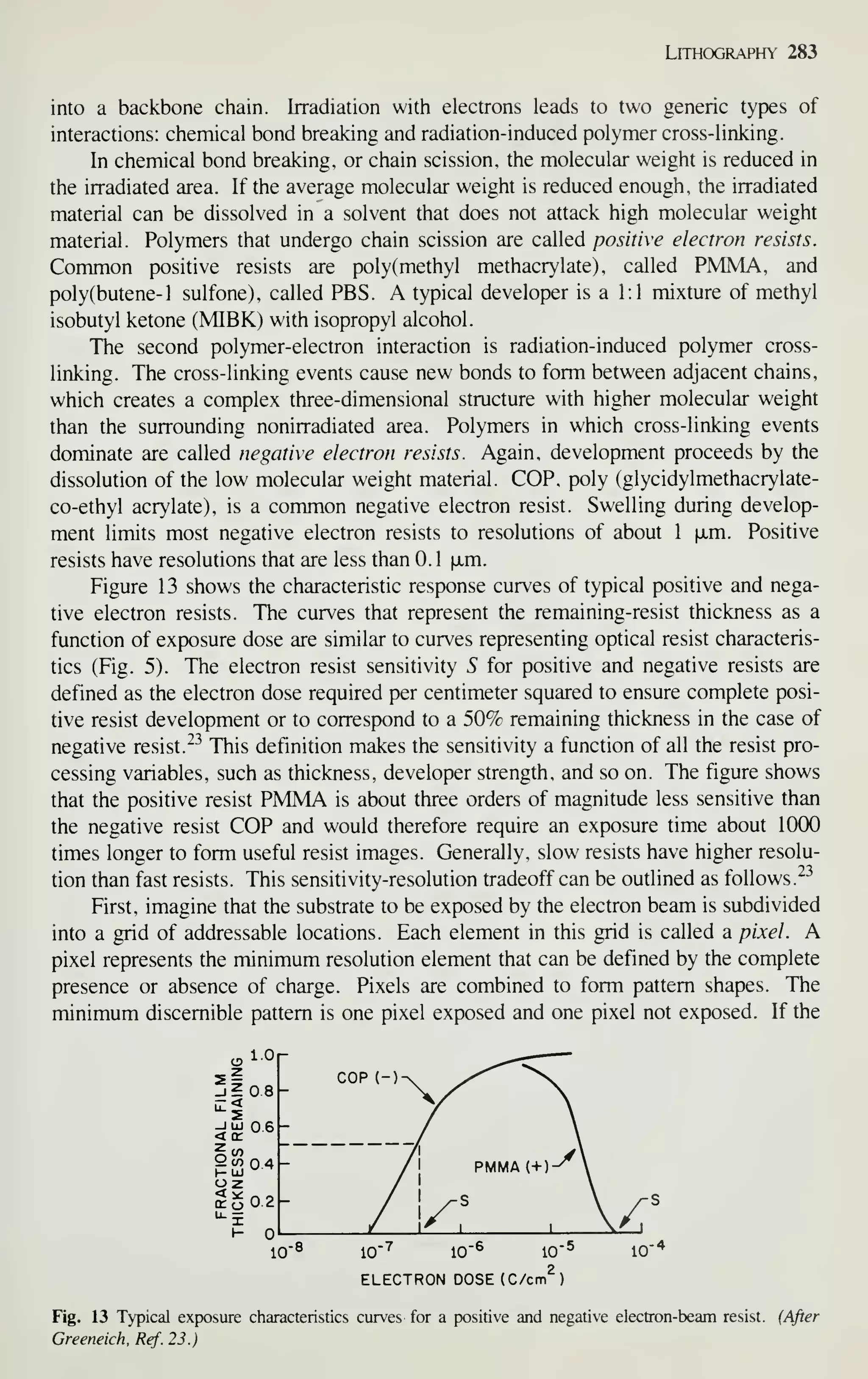
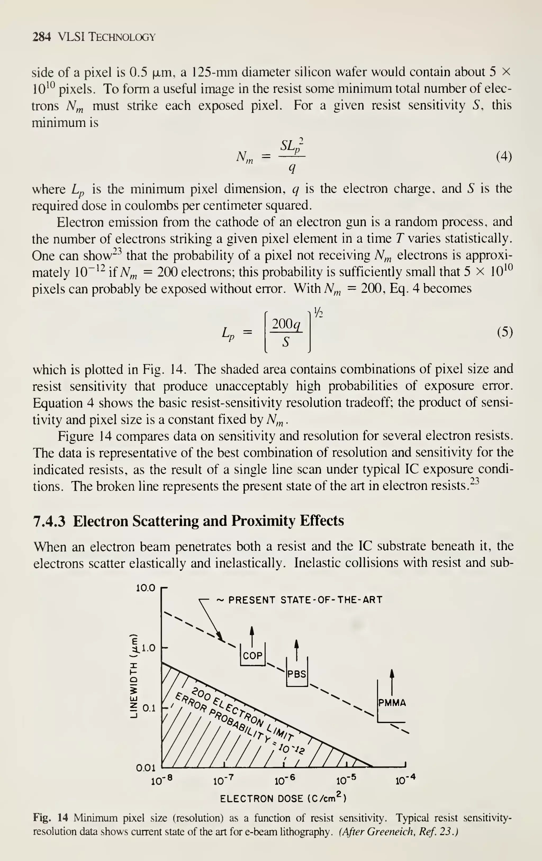
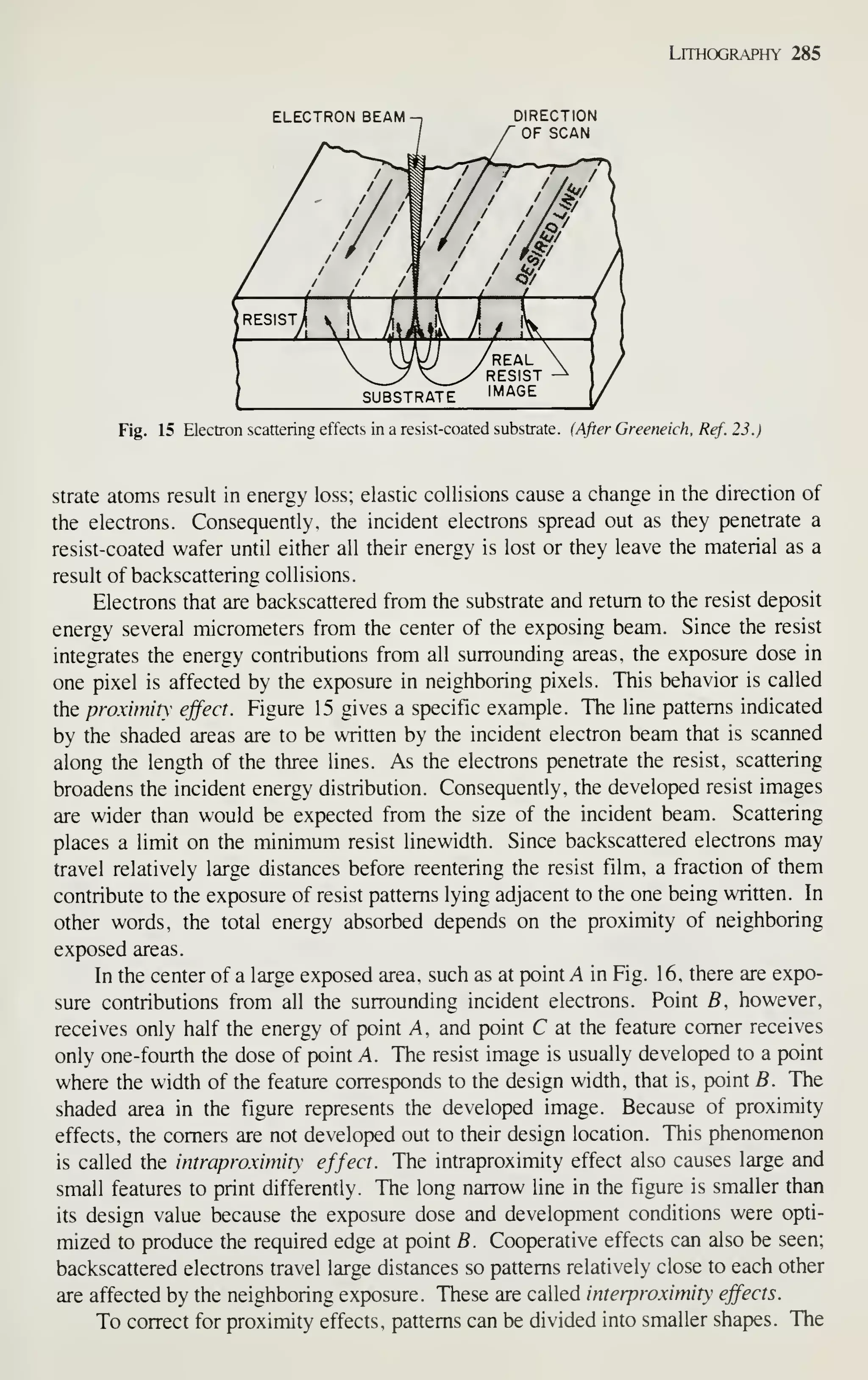
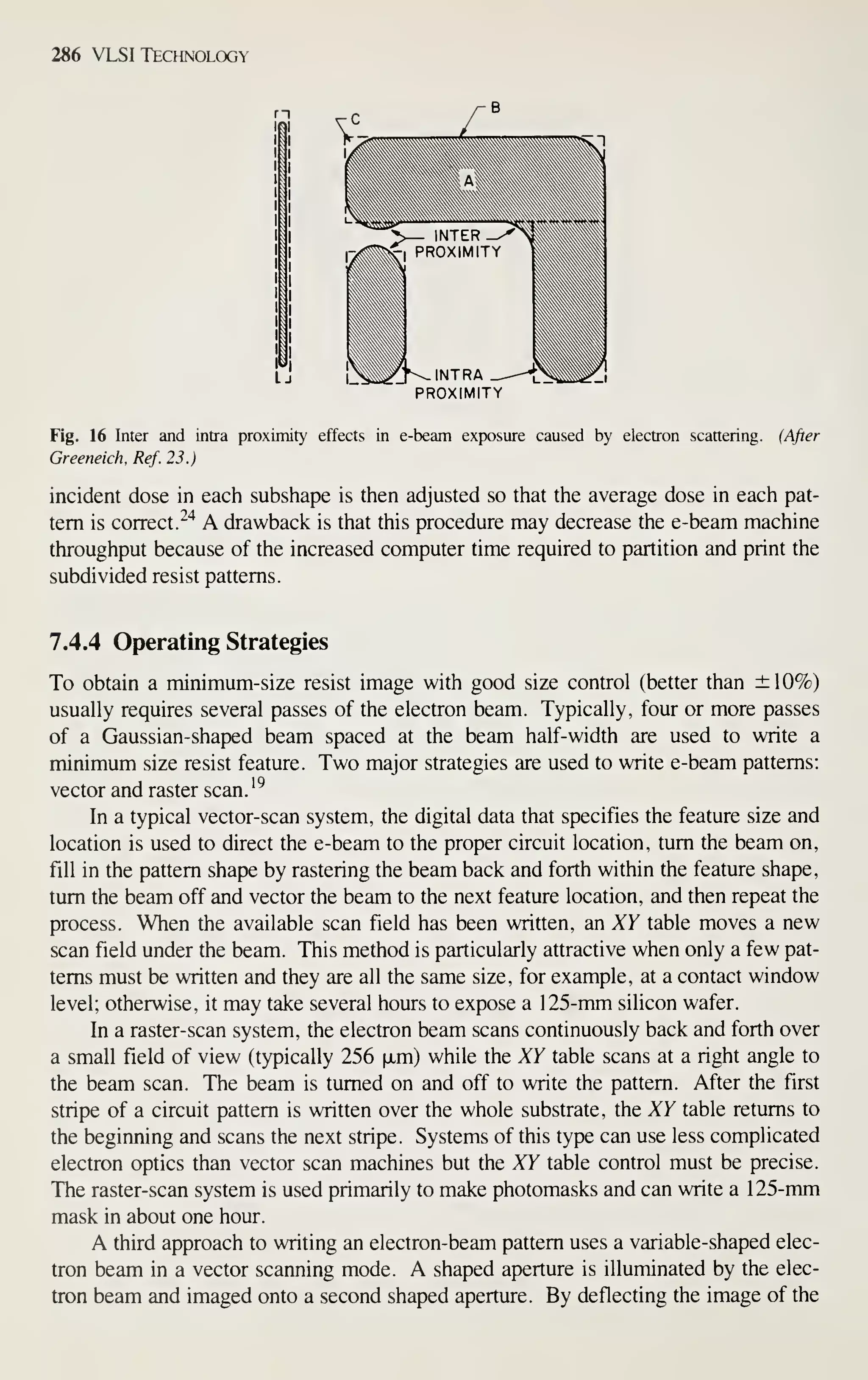
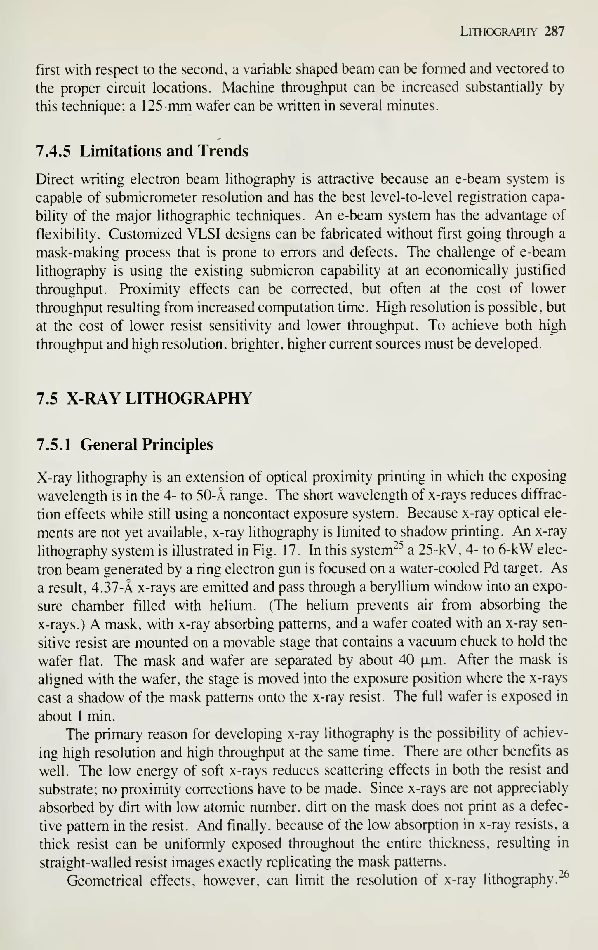
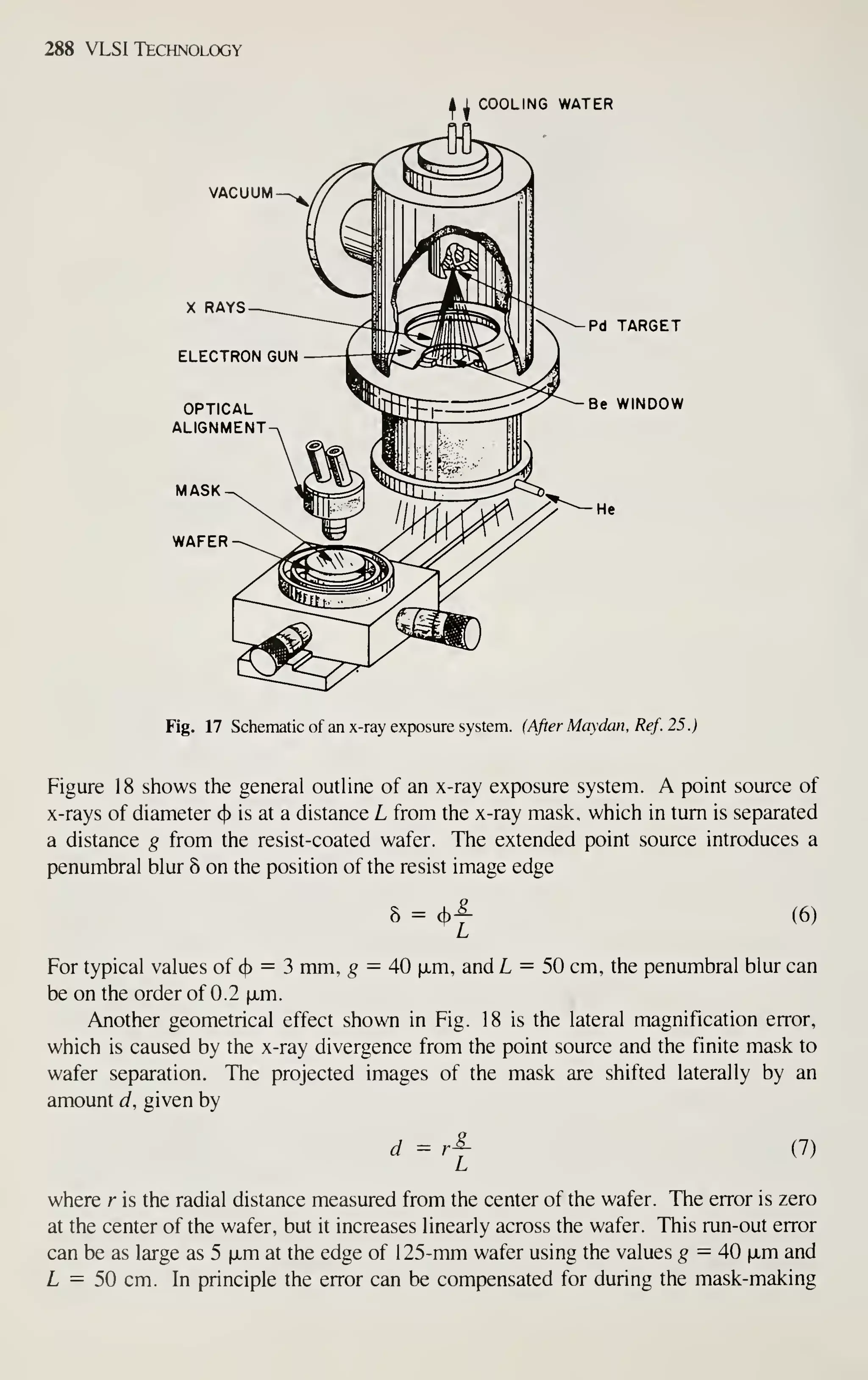
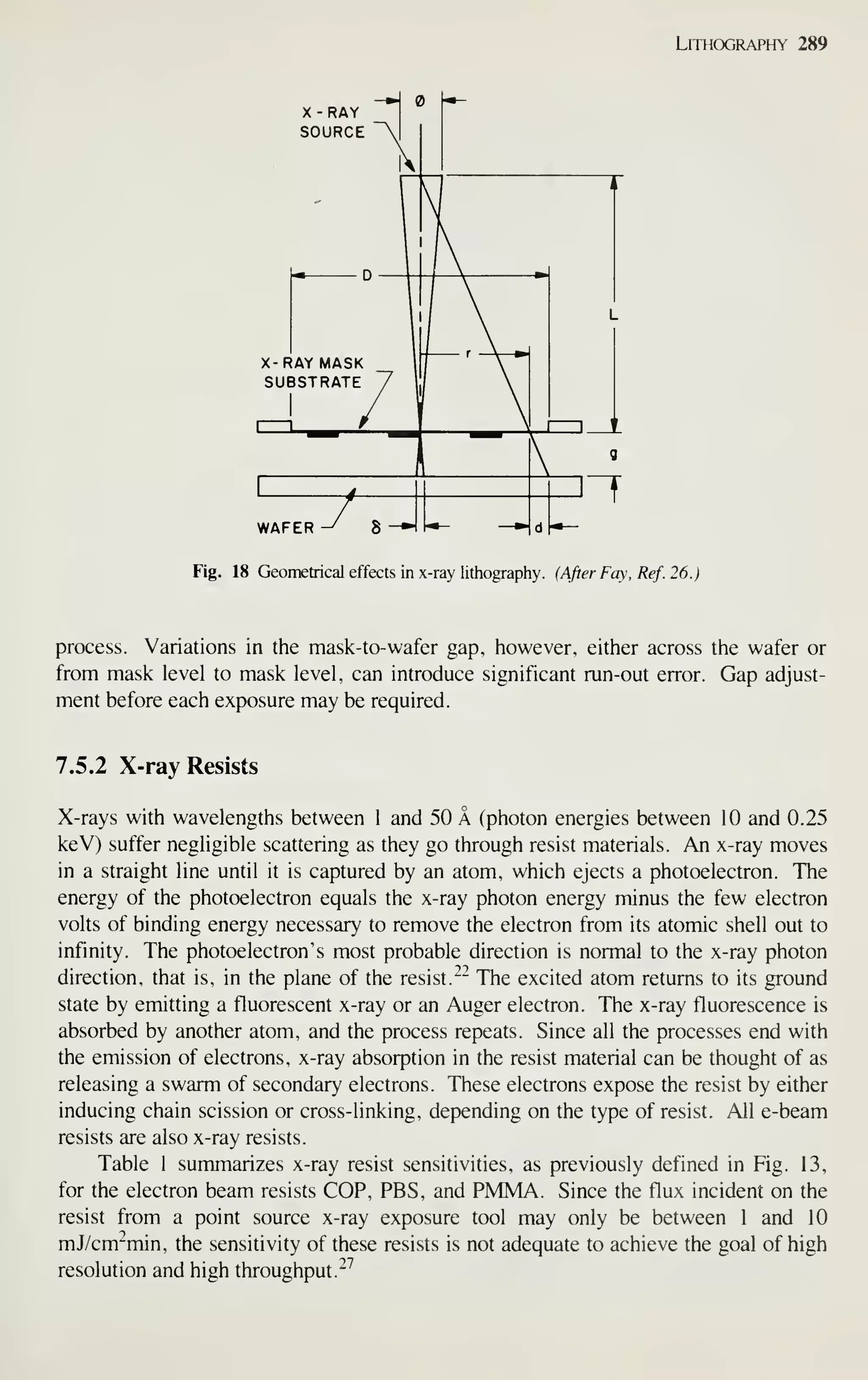
![290 VLSI Technology
Table 1 Properties of a few x-ray resists!
Resist Tone
Major Abs
elements K
Sensitivity
(mJ/cnr)
Resolution
(|jLm)
COP
PBS
PMMA
(-)
( + )
( + )
S
4.37APdi„
4.37APd^„
8.34AA1,„
175
94
600-1000
1.0
0.5
<0.1
tAfterTaylor, Ref. 27.
One way higher resist sensitivity can be accomphshed is by increasing the x-ray
absorption in the resist. The absorption of x-rays can be described by the equation
I = Iq exp (—ar) (8)
where t is the thickness of the resist, a is the linear absorption coefficient, and /q and
/ are the intensities before and after absorption, respectively. Figure 19 shows
absorption coefficients for a few selected materials"^ in the wavelength range of
interest. The absorption can be increased by increasing the absorption coefficient,
which is related to the x-ray atomic absorption cross sections of the elements in the
resist. The cross section for x-ray capture by electrons in a given atomic shell varies
with the x-ray wavelength and shows large increases at certain critical wavelengths.
The critical wavelengths correspond to x-ray energies that are just sufficient to
remove electrons from their atomic shells, K, L], and so on. For example,
wavelengths slightly longer than kj^ can no longer be captured by K-shell electrons;
therefore the cross section drops abruptly at that point. Materials are most transparent
Fig. 19 Absorption coefficients of PMMA, Be, Si, and Au in the x-ray wavelength range used in x-ray
lithography. (After Spiller and Feder, Ref. 28.)](https://image.slidesharecdn.com/simonm-220913174129-44ec6f82/75/Simon-M-Sze-editor-Very-Large-Scale-Integration-VLSI-Technology-McGraw-Hill-Inc-US-1983-pdf-310-2048.jpg)
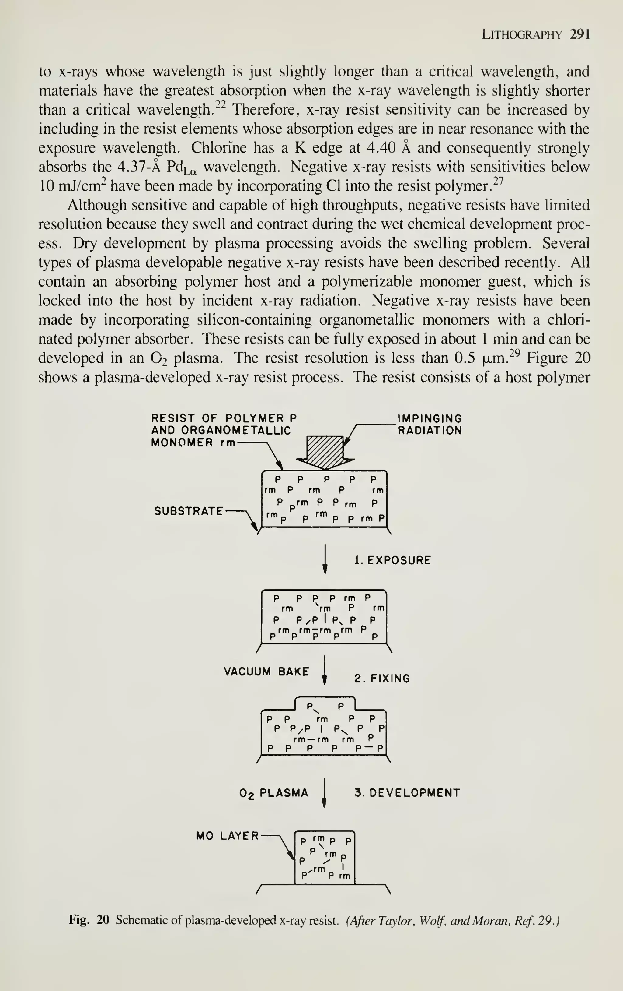

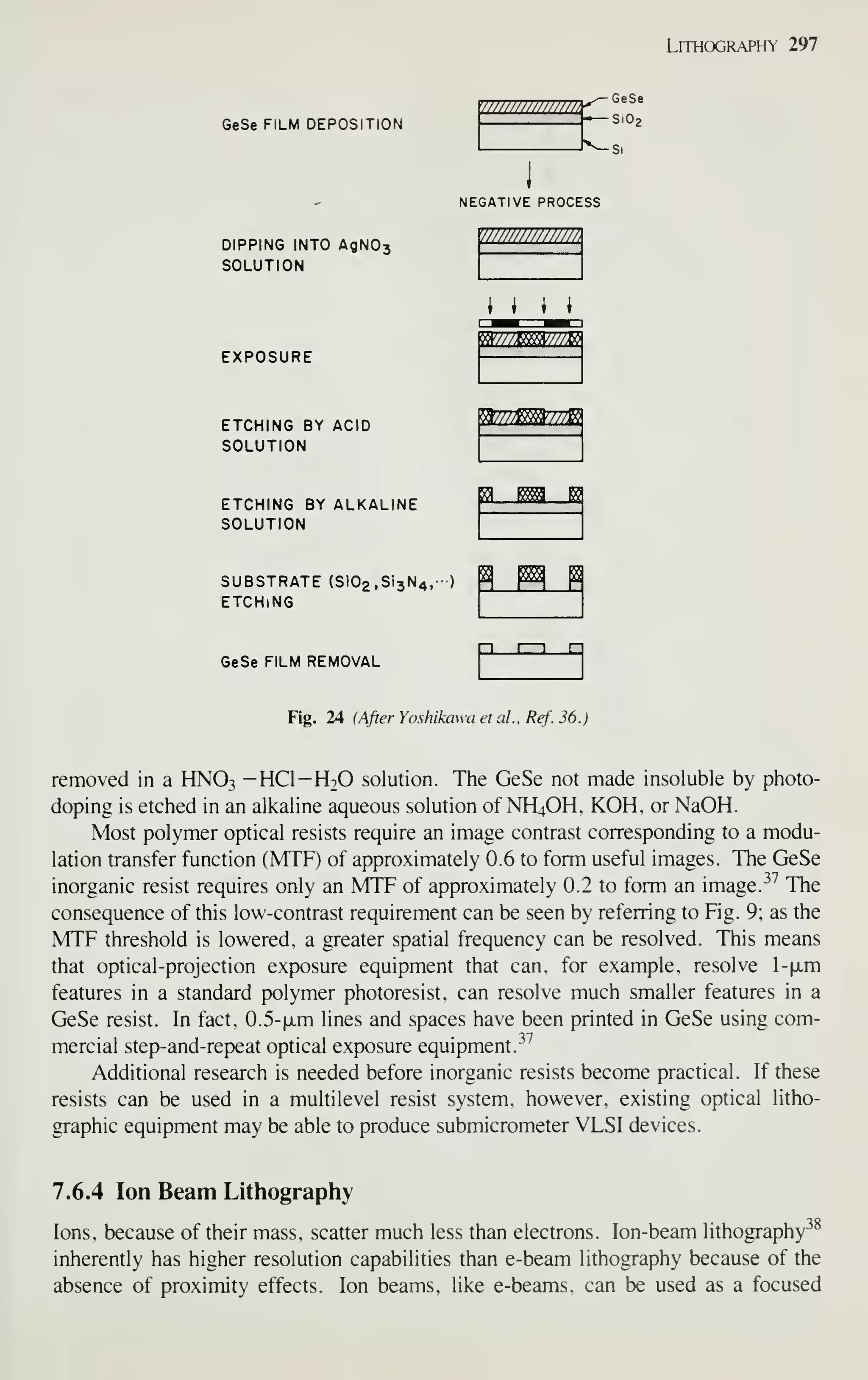
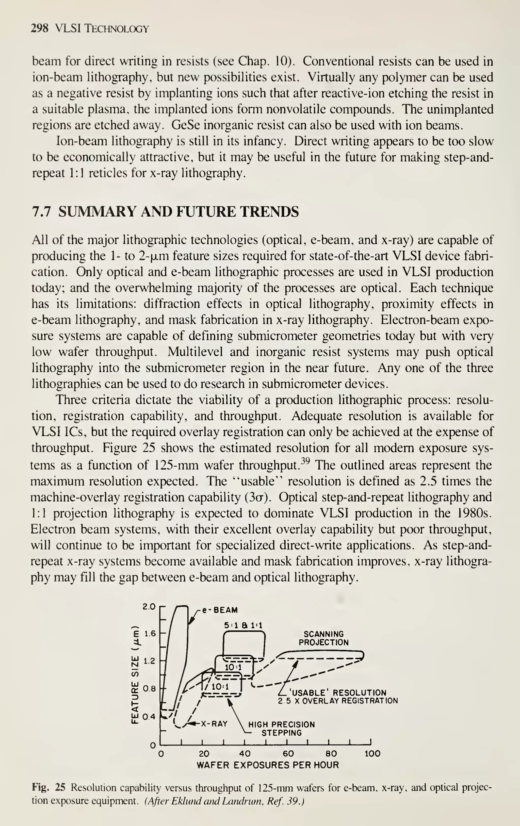
![300 VLSI Technology
[29] G. N. Taylor, T. M. Wolf, and J. M. Moran, "Organosilicon Monomers for Plasma-Developed X-
Ray Resists," J. Vac. Sci. Technol.. 19, 872 (1981).
[30] R. K. Watts, "X-Ray Lithography," Solid State Technol., p. 68, May 1979.
[31] See, for example, the series of papers by W. D. Buckley et al., 7. Electrochem. Sac, 128, 1 106-1 120
(1981).
[32] A. Heuberger, H. Betz, and S. Pongratz, "Present Status and Problems of X-Ray Lithography," in J.
Truesch (ed.). Advances in Solid State Physics. Plenary Lectures of the German Physical Society,
March, 1980.
[33] E. Chandross, E. Reichmanis, C. Wilkins, Jr., and R. Hartless, "Photoresists for Deep-UV Lithogra-
phy." Solid State Technol.:' p. 81, Aug. 1981.
[34] M. Hatzakis, "Multilayer Resist Systems for Lithography," Solid State Technol., p. 74, Aug. 1981.
[35] B. J. Lin, E. Bassous, V. Chao, and K. Pettillo, "Practicing the Novolac Deep-UV Portable Conform-
able Masking Technique," 7. Vac. Sci. Technol., 19, 1313 ( 1981).
[36] A. Yoshikawa, O. Ochi, H. Nagai, and Y. Mizushima, "A Novel Inorganic Photoresist Utilizing Ag
Photodoping in SeGe Glass Film," Appl. Phys. Lett., 29, 677 ( 1976).
[37] K. L. Tai, R. Vadimsky, C. Kemmerer, J. Wagner, V. Lamberti, and A. Timko, "Submicron Optical
Lithography Using an Inorganic Resist/Polymer Bilevel Scheme," J. Vac. Sci. Technol., 17, 1169
(1980).
[38] W. L. Brown, T. Venkatesan, and A. Wagner, "Ion Beam Lithography," Solid State Technol., p. 60,
Aug. 1981.
[39] M. H. Eklund and G. Landrum, "1982 Forecast on Processing," Semiconductor Int., p. 43, Jan.
1982.
PROBLEMS
1 Suppose that you are required to specify the resist thickness that will be used in a production lithographic
process. The following data is available:
• 1 .5-fjLm minimum features must be printed. Resolution is adequate when the resist thickness t is in the
range 0.5 to 2.0 iJim but feature size control is better for thinner resists.
• Each wafer has 150 chip sites; each chip has a 0.2-cm-^ active area.
• 5 mask levels are required to complete the device.
• 2000 finished wafers must be produced each day (20 h per day = 3 shifts).
• The resist defect density Dq increases as the resist is made thinner, where Dg is the number of defects
per square centimeter, and is approximated by D q = 1 -4 /
~^; t is in micrometers.
• The chip yield (percentage good) can be approximated at each mask level by v = (1 + ^Dga)"'.
where q is the fraction of defects that render a chip inoperable (fatality rate) and a is the active area of
the chip.
• On average, 50% of the defects are fatal defects.
• More time is needed to expose thick resist than to expose thin resist. The exposure tool throughput in
wafers/h is approximated by 125 - 50r for (0.5 « f « 2.0 (xm).
ia) Specify the resist thickness to be used and justify your recommendation with tabular and graphical
data.
(b) If exposure tools cost $350,000 each, what is the difference in equipment cost for a process using
1 ^.m and 1 .5 xm of resist.
2 Referring to Fig. 10, assume that the amplitude of the incident light wave £2 is given by
^^.(.v) = £2 sin iwt - kx + (J))
and the amplitude of the reflected wave £3 is given by
Ei,{x) = E2 sin [wt - k{2d - x) + <i>
+ -n]](https://image.slidesharecdn.com/simonm-220913174129-44ec6f82/75/Simon-M-Sze-editor-Very-Large-Scale-Integration-VLSI-Technology-McGraw-Hill-Inc-US-1983-pdf-320-2048.jpg)
![Lithography 301
where k = l-nn/X. n is the real part of the film dielectric constant and is assumed equal for photoresist and
SIOt. and is the exposing wavelength.
(a) Referring to Fig. lOr. derive an expression for the standing wave intensity attributable to the
interference between Ei and E i,.
(b) Derive equations that predict the positions of the intensity minima and maxima with respect to the
reflecting surface.
(c) Consider a positive photoresist film on 1250 k of SiOi over a silicon substrate. Discuss the effect
on the resist image that might result from a SIOt thickness change of ±250 A. Assume n = 1.6 and =
3200A.
3 In electron beam lithography the term Gaussian beam diameter (cIq ) describes the diameter of an electron
beam in the absence of system aberrations, that is, a beam distorted only by the thermal velocities of the
electrons. The current density in a Gaussian beam is given hy J = J^ exp [— (r/a)"], where y„ is the peak
current density, r is the radius from the center of the beam, and a is the standard deviation of electron distri-
bution in the beam. Defining dQ = 2a, derive an expression relating d(j to the peak current density y„ and
the total current in the electron beam /.
Answer: I = (-u lAXJ^dQ
4 The maximum current density 7,,, that can be focused toward a spot with a convergence half-angle a is
limited by the transverse thermal emission velocities of the electrons in a Gaussian electron beam. J,„ is
given by the Langmuir limit equation
eVo
^ ^ AT.
where 7,, is the cathode (source) current density, T^ is the temperature corresponding to the electron energy,
k is Boltzmann's constant (1.38 x 10~-^^J/°K), and e is the electronic charge (1.6 x 10"''^ C). For small
convergence angles a, derive an expression that relates the Gaussian beam diameter dQ to the electron
source parameters 7^, , 7"^- , and Vq.
Answer: d^ ^ IkT^J[{TT/4)J^-eVQa-]
5 {a) The brightness fi of a source of electrons is defined as the current density J emitted per unit solid
angle H, that is, B = J /Ci. The units of B are amperes per square centimeter per steradian. Assume that
the current is emitted from (or converges toward) a small area through a cone of included half-angle a and
that a is small. Derive an expression relating the maximum source brightness to the source parameters J^ ,
T^ , and Vq.
Answer: B =J^eVQ/TTkT^
(b) Assuming that brightness is conserved in the electron beam column, show that the Gaussian beam
diameter dQ is related to the source brightness.
Answer: dQ = {2
/
-nXl / a){I / B y~
6 Suppose that an x-ray resist must see a mask modulation greater than or equal to 0.6 in order to form use-
ful resist images. What is the minimum gold thickness required on an x-ray mask to satisfy this requirement
if the exposure wavelength is 4 A ?
Answer: t ^0.31 xm](https://image.slidesharecdn.com/simonm-220913174129-44ec6f82/75/Simon-M-Sze-editor-Very-Large-Scale-Integration-VLSI-Technology-McGraw-Hill-Inc-US-1983-pdf-321-2048.jpg)

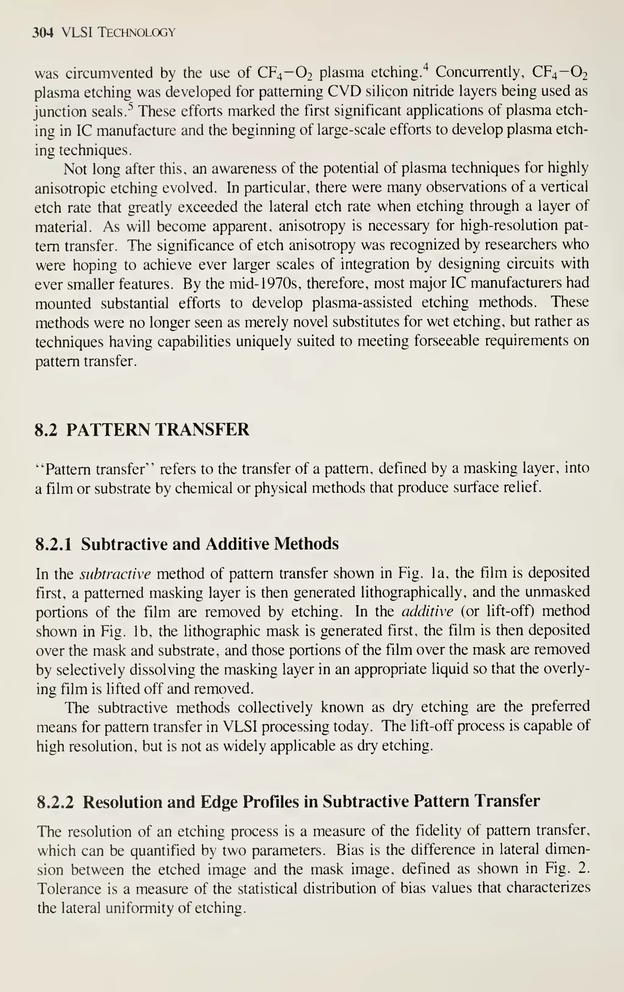
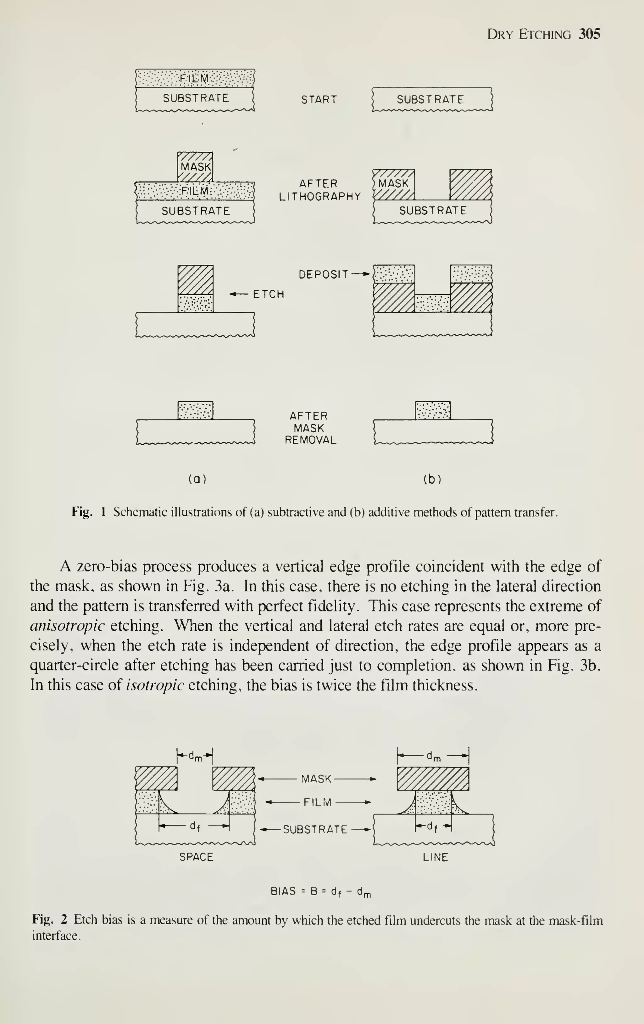
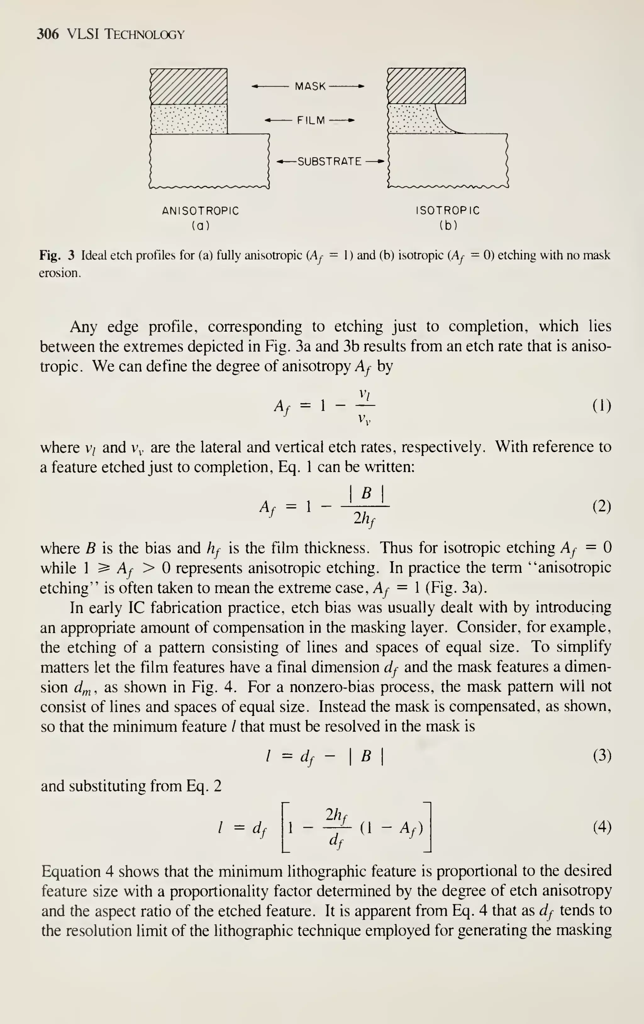
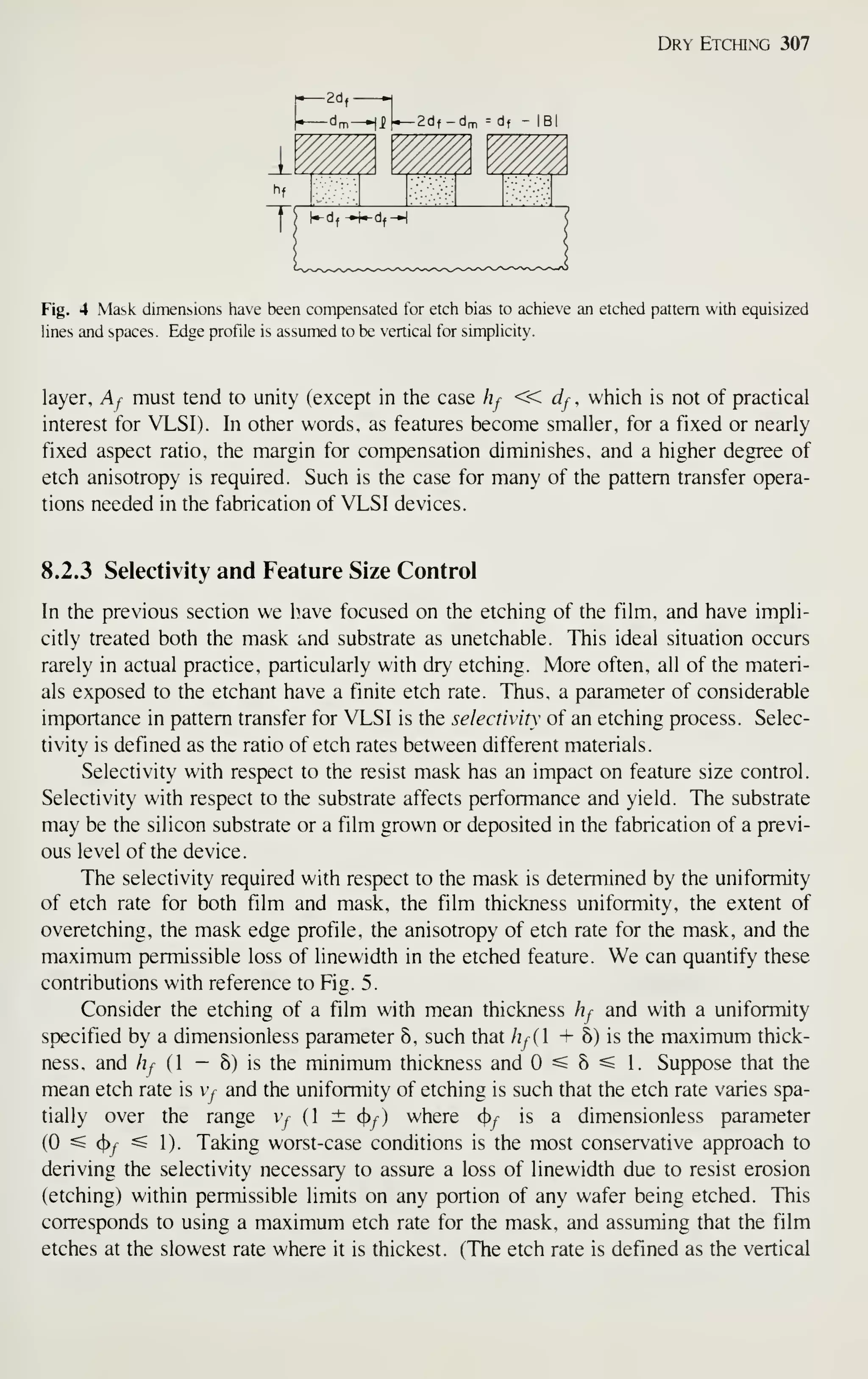
![308 VLSI Technology
Fig. 5 The evolution of an etched feature when the mask has a finite etch rate. The difference between the
intended pattern width and the actual linewidth is W.
depth of etching divided by the time of etching.) In this region of the film the time to
complete etching f^ is:
hf (1 + 8)
t = —
v^ (l-<j>/)
(5)
If A is the fractional overetch time, the time to completion is extended to r,,(l + A),
so that the total etch time r, is:
hf (1 + 8) (1 + A)
t,
= (6)
vy (1 - 4)/)
During this time, the mask is eroded by etching as shown in Fig. 5. If the mask
has maximum vertical and lateral etch velocities v and v/ , respectively, then the edge
of the mask recedes by a maximum amount W /2 given by:
W = [vy cot e + v/ ]t, (7)
where is shown in Fig. 5. Substituting for r, from Eq. 6 we find after rearrange-
ment:
V (1 + 8) (1 + A)
Vf ^ (l-cj)/)
cot e + — (8)
The etch rate of the mask is defined by the vertical etch velocity. In the present case](https://image.slidesharecdn.com/simonm-220913174129-44ec6f82/75/Simon-M-Sze-editor-Very-Large-Scale-Integration-VLSI-Technology-McGraw-Hill-Inc-US-1983-pdf-328-2048.jpg)
![Dry Etching 309
V,. has been taken as a maximum value, thus providing the most conservative estimate
of the selectivity required for a given value of W.
We can define the mask etch rate in terms of a uniformity parameter cj)^ such that
. = 'm( + (}),„) where v^ is the mean mask etch rate. Then noting that
vy/v. = Sfm is the desired selectivity of the film with respect to the mask, and
v/ /v. = - A^ where A,„ is the degree of etch anisotropy for the mask, Eq. 8 can
be rearranged to yield:
^/- =
i^
^>[^°^ e + (1 - A,„)l (9)
where Uf^ = [H + 8) (1 + A) (1 + (t),„)]/(l -(})/) is the "'uniformity" factor
that accounts for a worst-case coincidence of the various nonuniformities.
It is instructive to consider an example that illustrates the application of Eq. 9.
Suppose that etching is carried out using a process that is fully anisotropic for the film
(Ay = 1). In this case the only linewidth loss results from resist erosion. Further, let
us assume that the etch rate uniformity for both film and mask is 10%, that the film
thickness uniformity is 5%, and that a 20% overetch is used. Then we have:
^f
= <t>,„
= 0.1, 8 = 0.05. and A = 0.2. Substituting these values in Eq. 9 we
find,
Sf„, = 1.54 [cote + (1 - A^)] -^ (10)
Figure 6 shows a plot of this expression for the particular cases 6 = 60° and 90°, and
for isotropic and fully anisotropic etching of the masking layer. For photoresist
masks, the angle is determined by the lithographic method (Secfion 7.3.1) and can
be influenced by post-exposure processing. An angle of 60° is typical for scanning-
type projection printers whereas 6 of about 90° can be achieved with contact printing.
Vertical walled masks (0 = 90°) are also typical of multilevel resist systems (Section
7.6.3). Note that the most favorable case for linewidth control corresponds to aniso-
tropic etching of a vertical-wall mask. This ideal is approached when multilevel
resists are used in conjunction with reacfive ion etching processes (Secfion 8.4).
The selectivity required with respect to etching of the substrate material can be
determined by an approach analogous to the one just used for the mask. Again, tak-
ing the conservative, worst-case view that the fastest etching and thinnest portion of
the film overlays the fastest etching portion of the substrate, we find:
h
Sfs = ir^fs (11)
where h^ is the maximum permissible depth of penetration into the substrate and
'(t)/(2 + A + A8) + 8(2 + A) + A
^fs =
(1 - c})/)
with c})y^, A, and 8 defined as before.
(12)](https://image.slidesharecdn.com/simonm-220913174129-44ec6f82/75/Simon-M-Sze-editor-Very-Large-Scale-Integration-VLSI-Technology-McGraw-Hill-Inc-US-1983-pdf-329-2048.jpg)
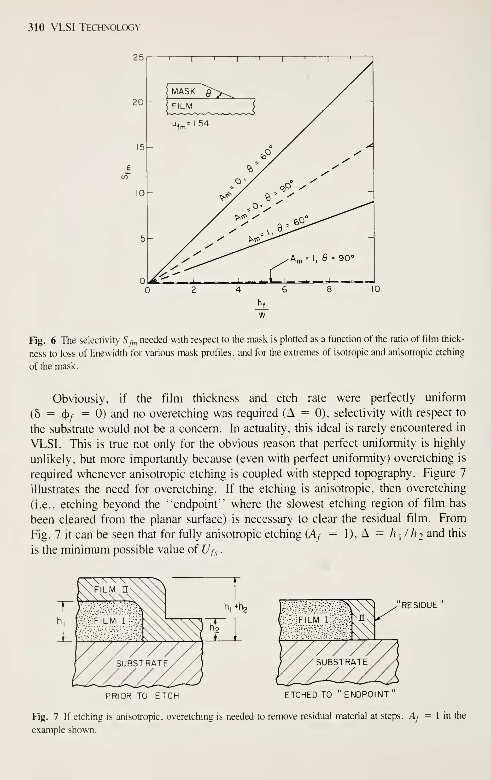
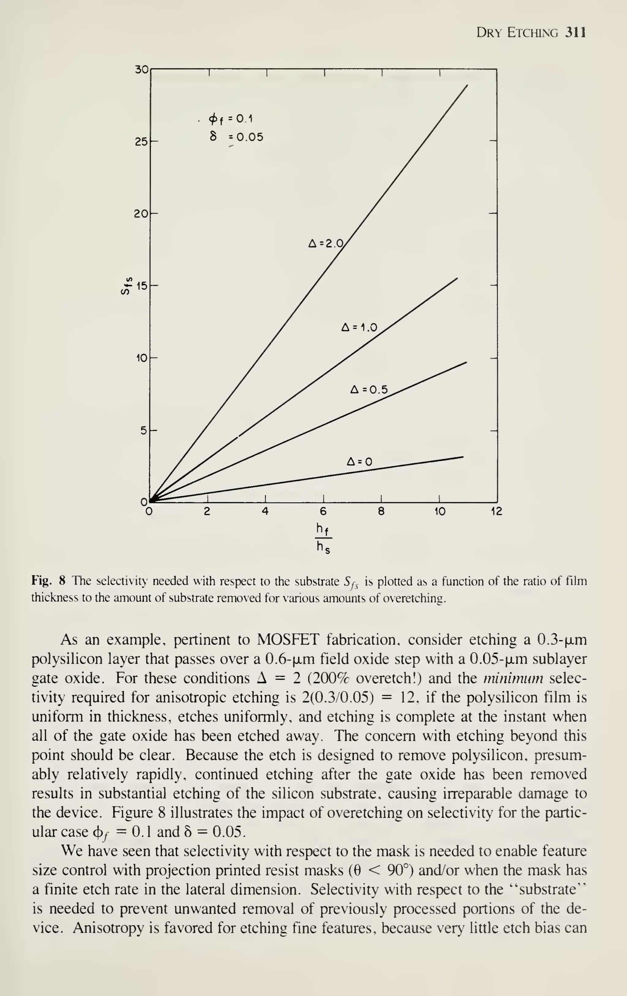
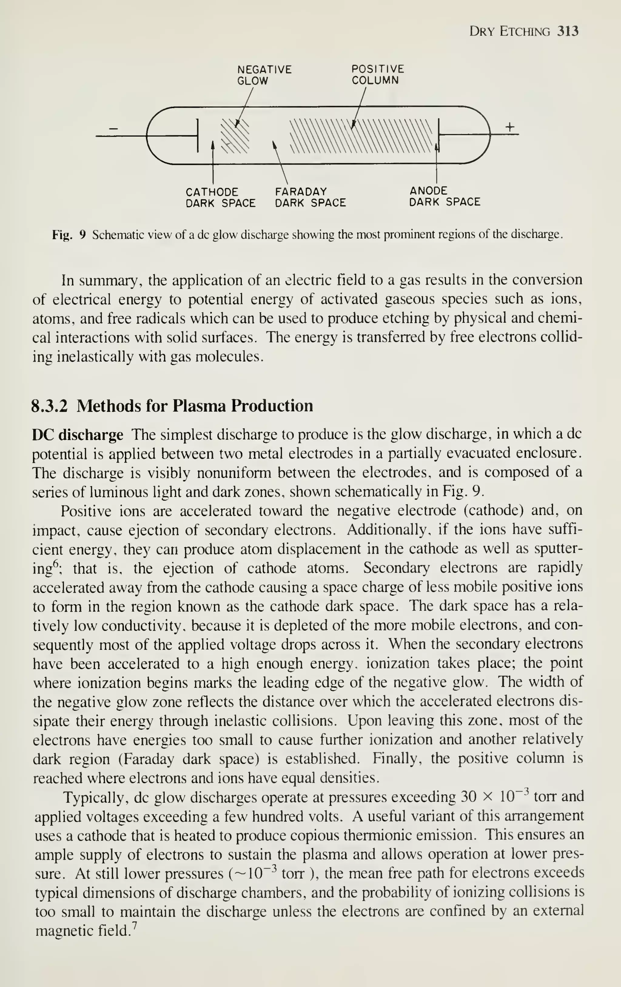
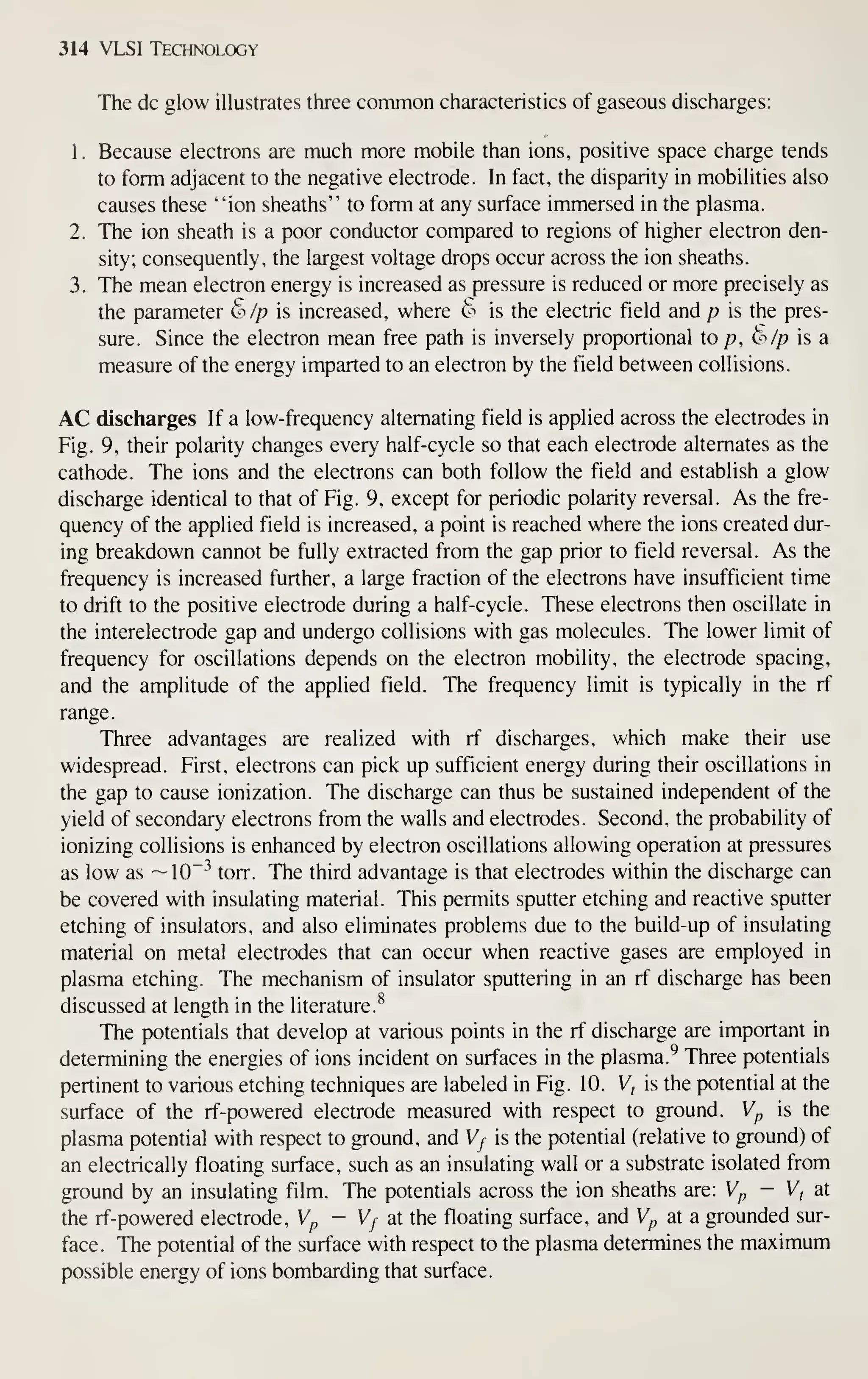
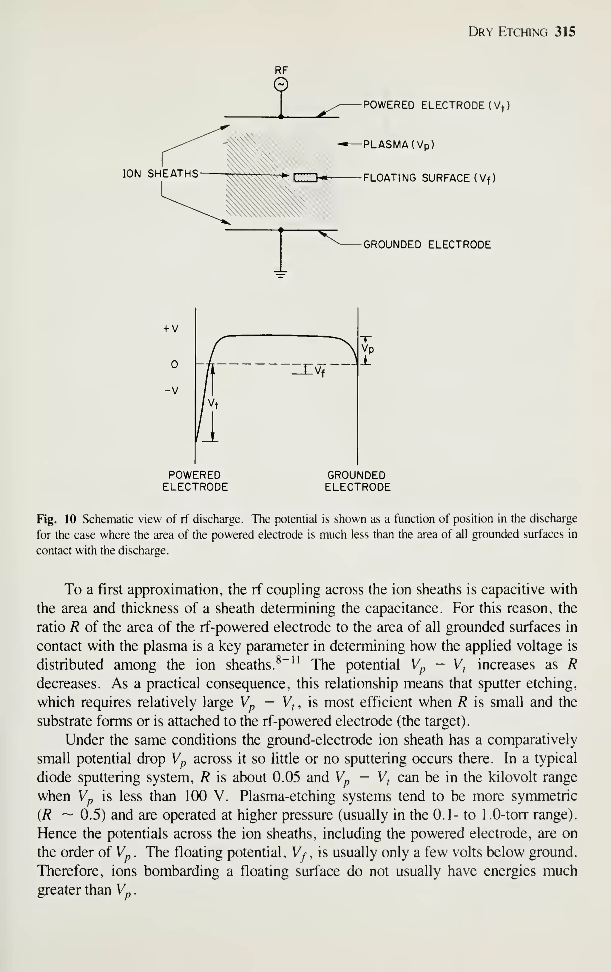
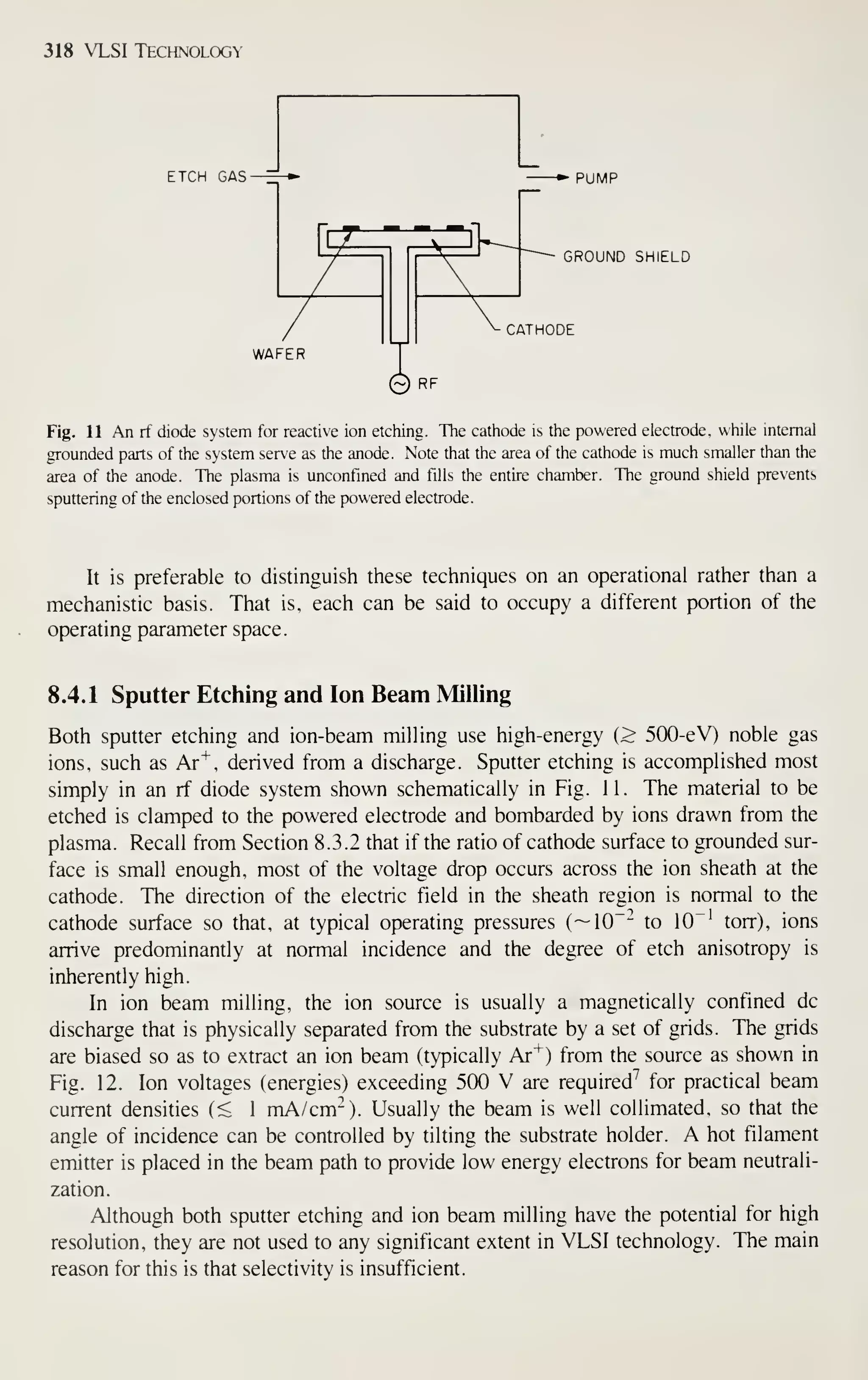
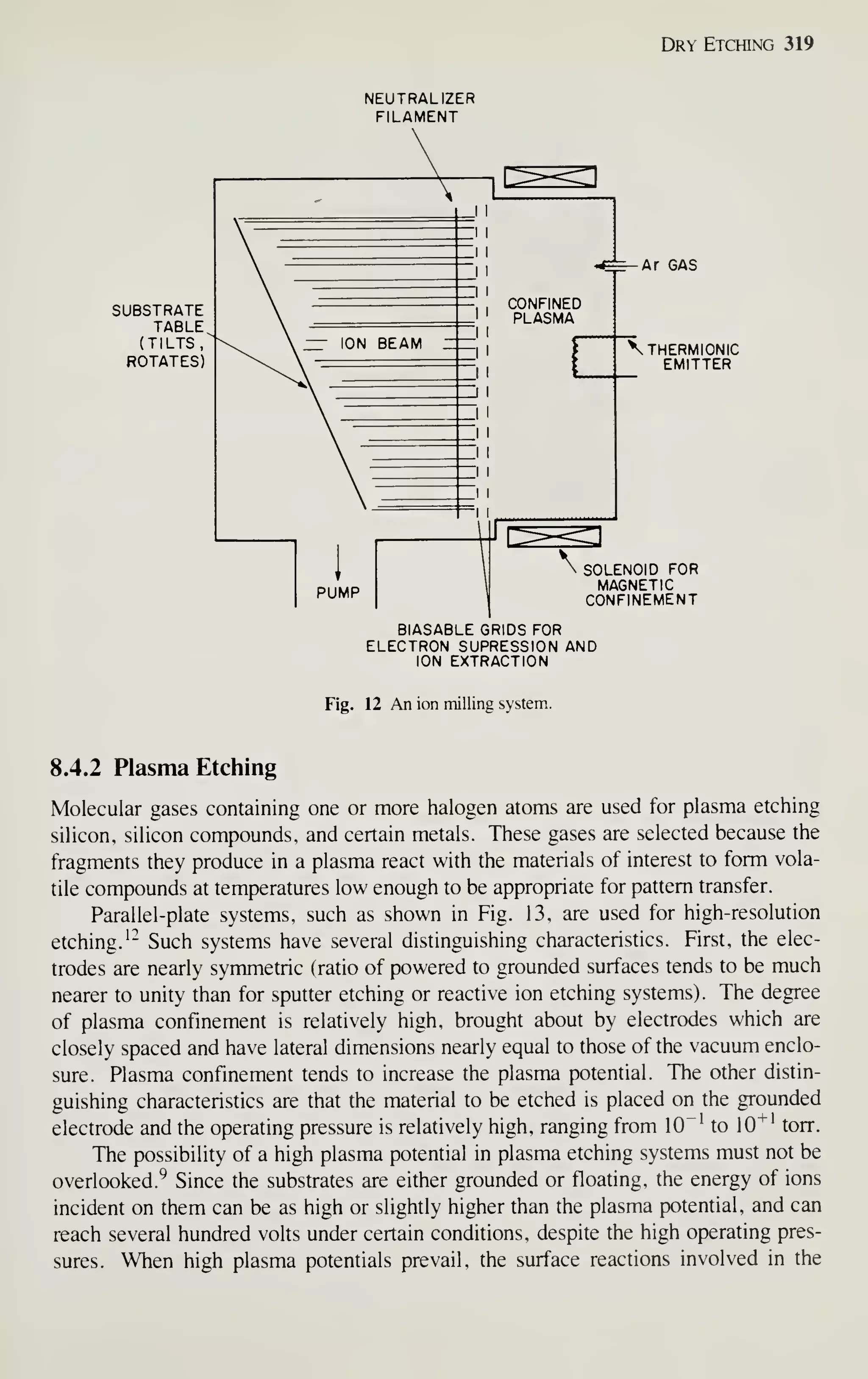
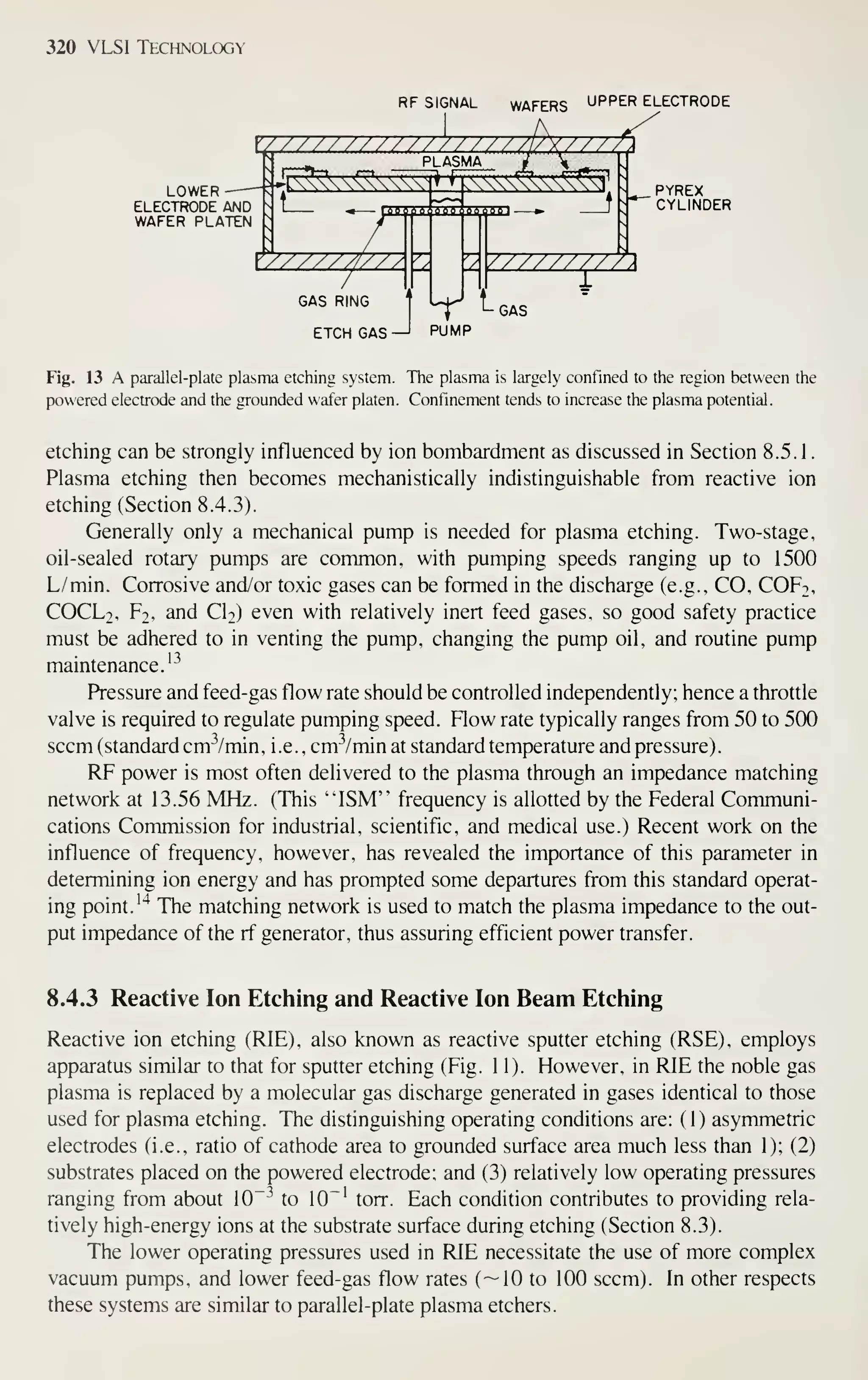
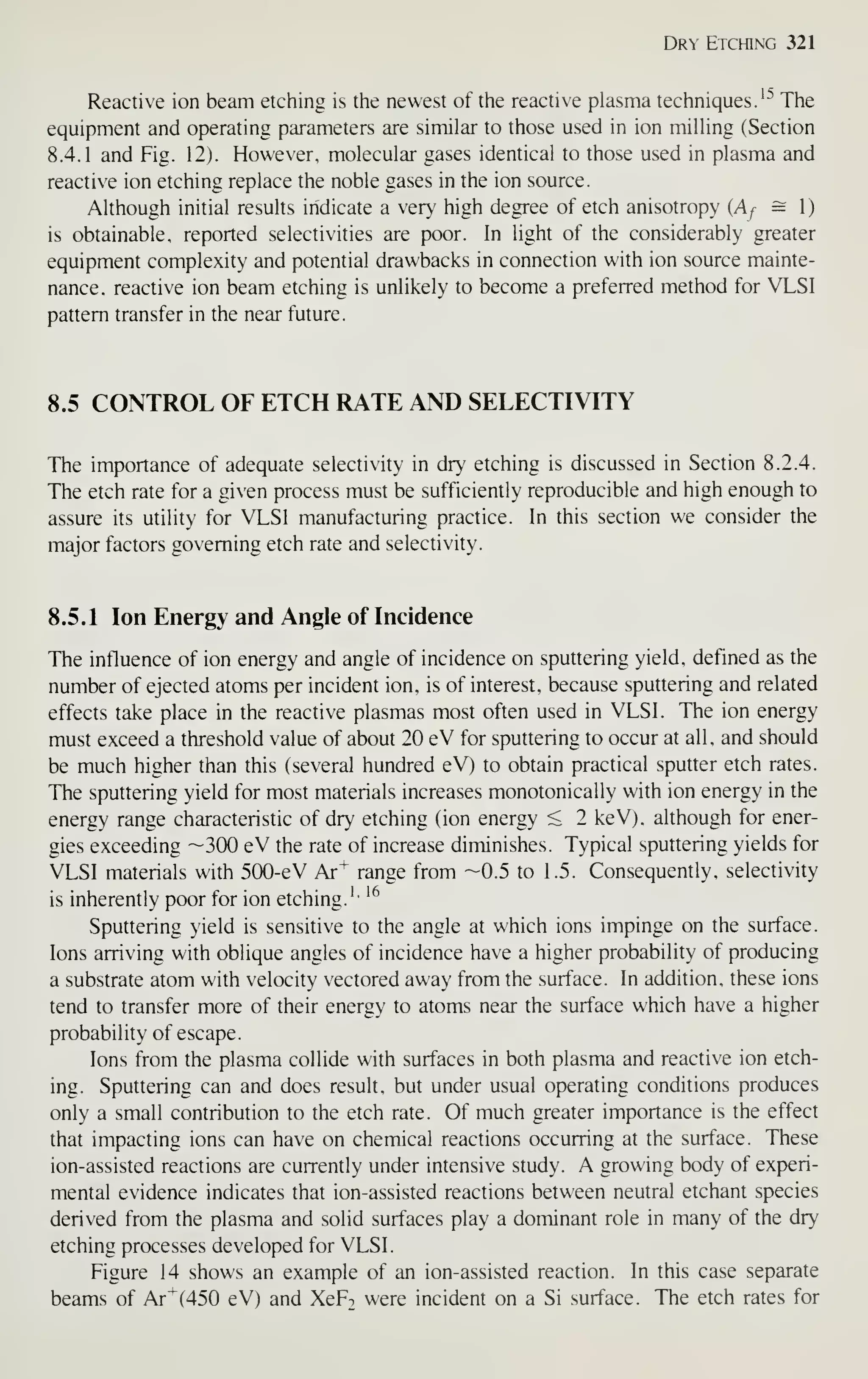
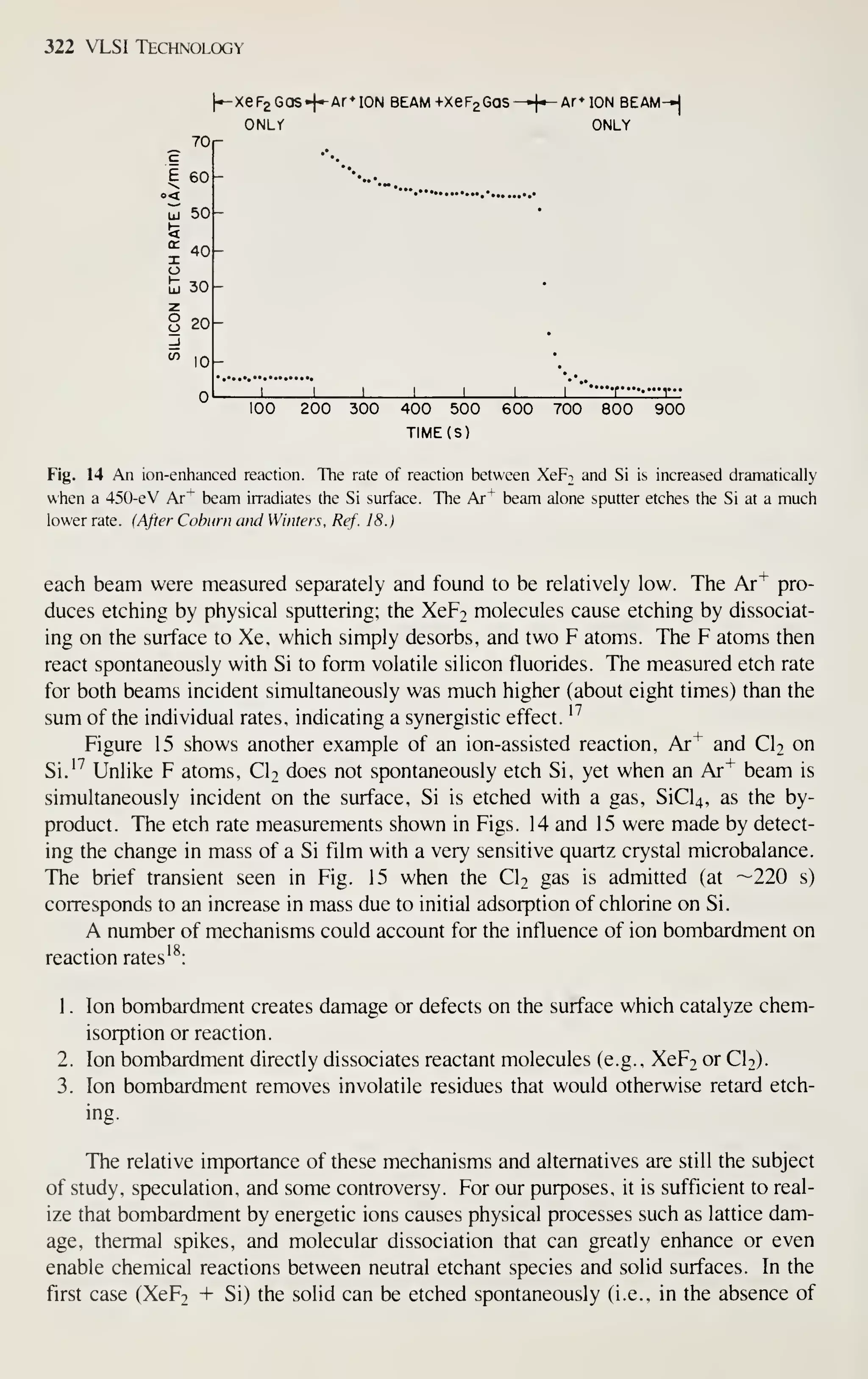
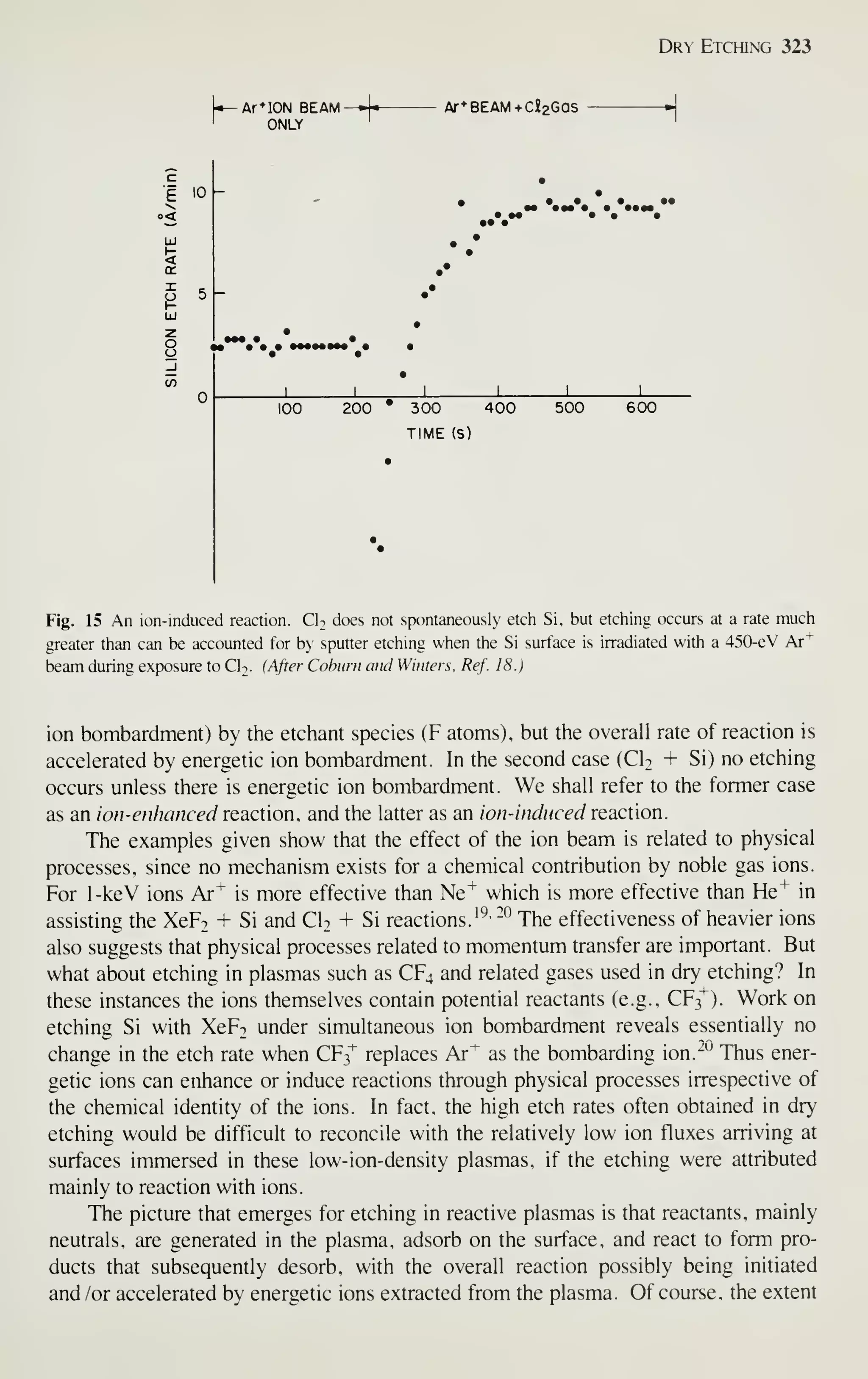
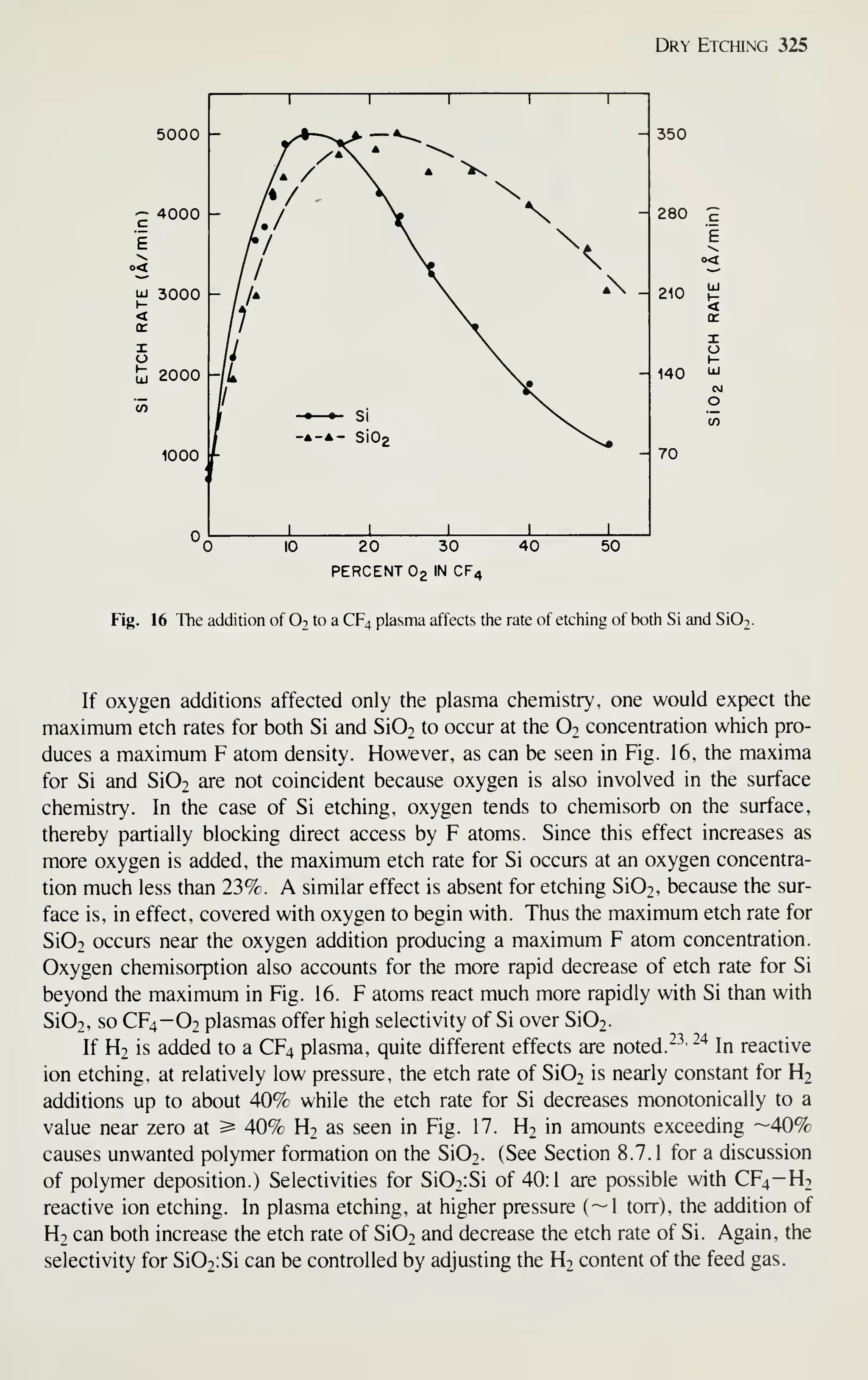
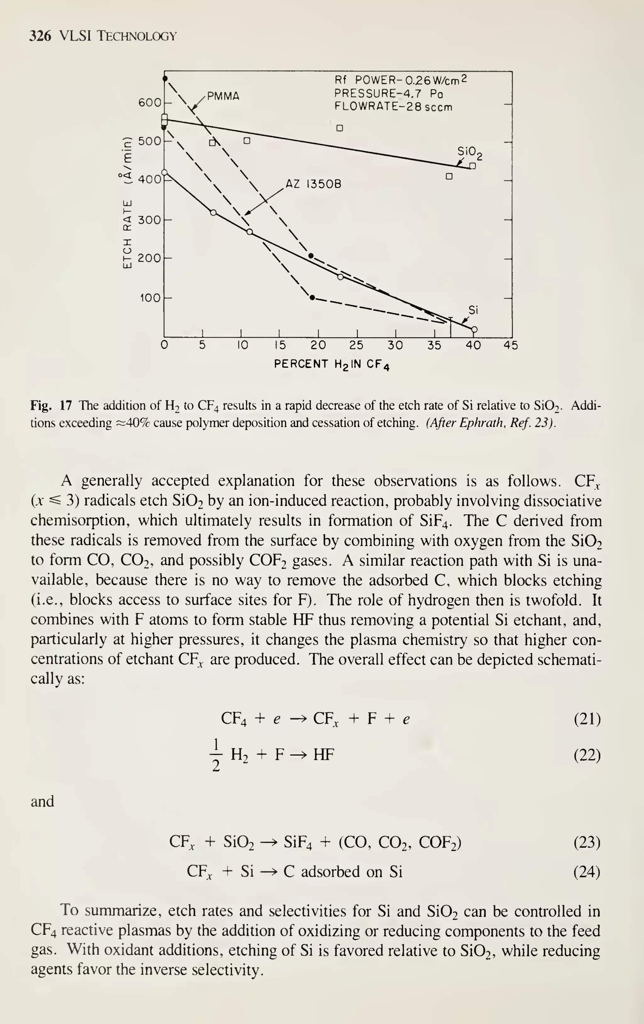
![328 VLSI Technology
100 200 300
FLOW RATE (cm^/min)-
400
Fig. 18 The reciprocal of etch rate R is linear in flow rate for etching in a CF4—4% O2 plasma at 1 .0 torr.
This dependence indicates that the lifetime of the active species is determined by convective losses. (After
Kalter artd Van deVen. Ref. 27.)
8.5.5 Temperature
Temperature influences etch rate in reactive etching primarily through its effect on the
rates of chemical reactions. An Arrhenius dependence [etch rate ~ exp {—Q/kT)
where Q is the activation energy, T is the absolute temperature of the substrate, and k
is Boltzmann's constant] usually prevails with relatively small values of activation
energy (Q ^ 0.5 eV/mole), although exceptions have been noted where the rate
decreases with temperature."^^ The rate decrease may be due to an increase in the rate
of thermal desorption of etchant species from the surface. Selectivity can also be
affected by temperature because the activation energy is material-dependent.
Some means of controlling substrate temperature is desirable for obtaining uni-
form and reproducible etch rates. Heating by the plasma is a major source of tem-
perature rise in thermally isolated wafers. In addition, the heat generated from exo-
thermic reactions that produce etching can be appreciable. Figure 19 illustrates the
effect of the heat of reaction on wafer surface temperature during the stripping of pho-
toresist in a barrel reactor,' where wafers are relatively isolated thermally. The max-
ima in the curves correspond to the times when resist stripping is completed. The
shift in the positions of the maxima with wafer load is due to the loading effect dis-
cussed in the next section.
8.5.6 The Loading Effect
In reactive etching the etch rate is sometimes found to decrease as the amount of etch-
able surface area is increased. This phenomenon is known as the loading effect.
Loading occurs when the active etch species reacts rapidly with the material being
etched, but the species has a long lifetime in the absence of etchable material. Etch-
ing is then the primary loss mechanism for the species, so the greater the area of
material, the more etchant species are consumed. The generation rate of the active](https://image.slidesharecdn.com/simonm-220913174129-44ec6f82/75/Simon-M-Sze-editor-Very-Large-Scale-Integration-VLSI-Technology-McGraw-Hill-Inc-US-1983-pdf-348-2048.jpg)
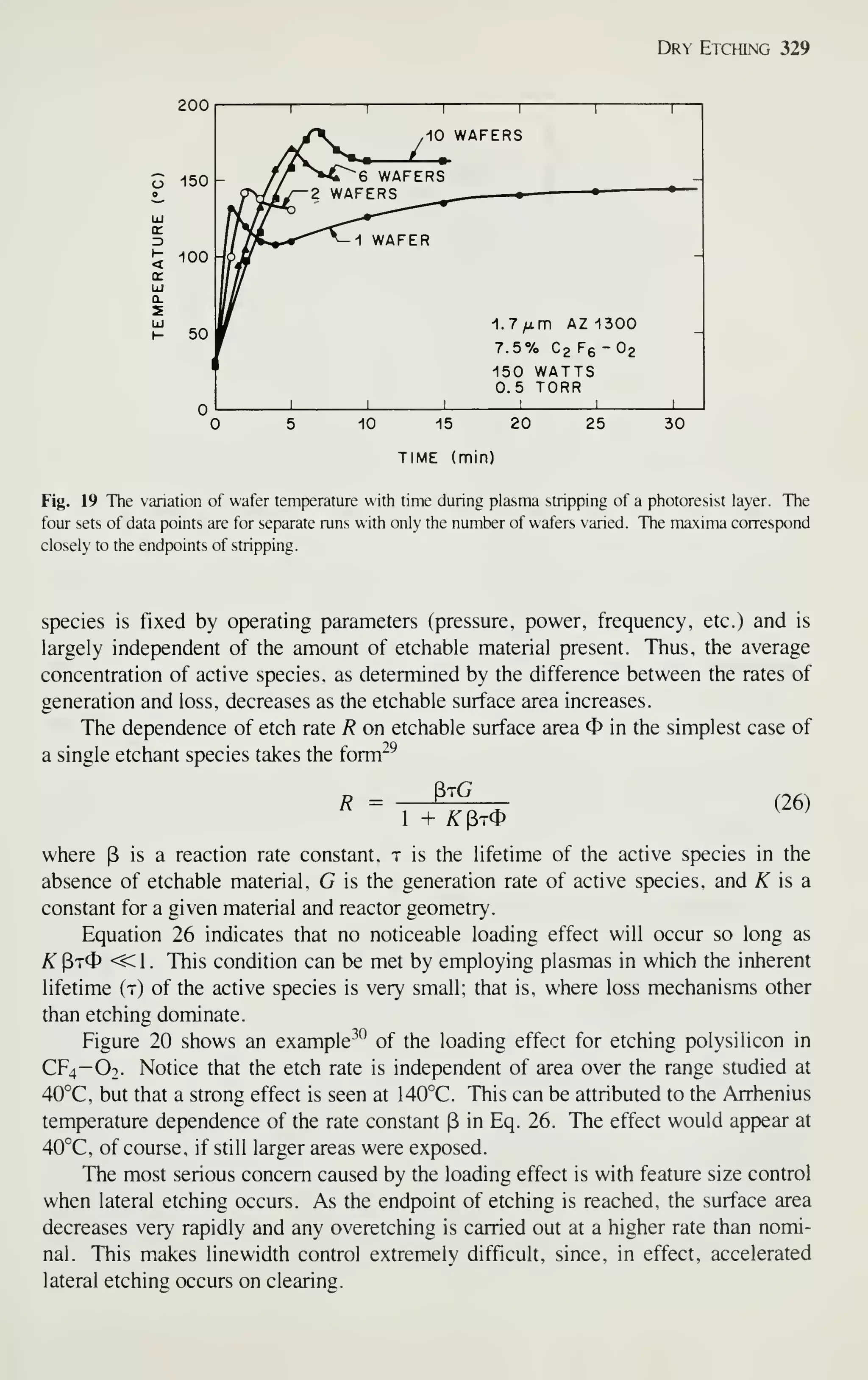
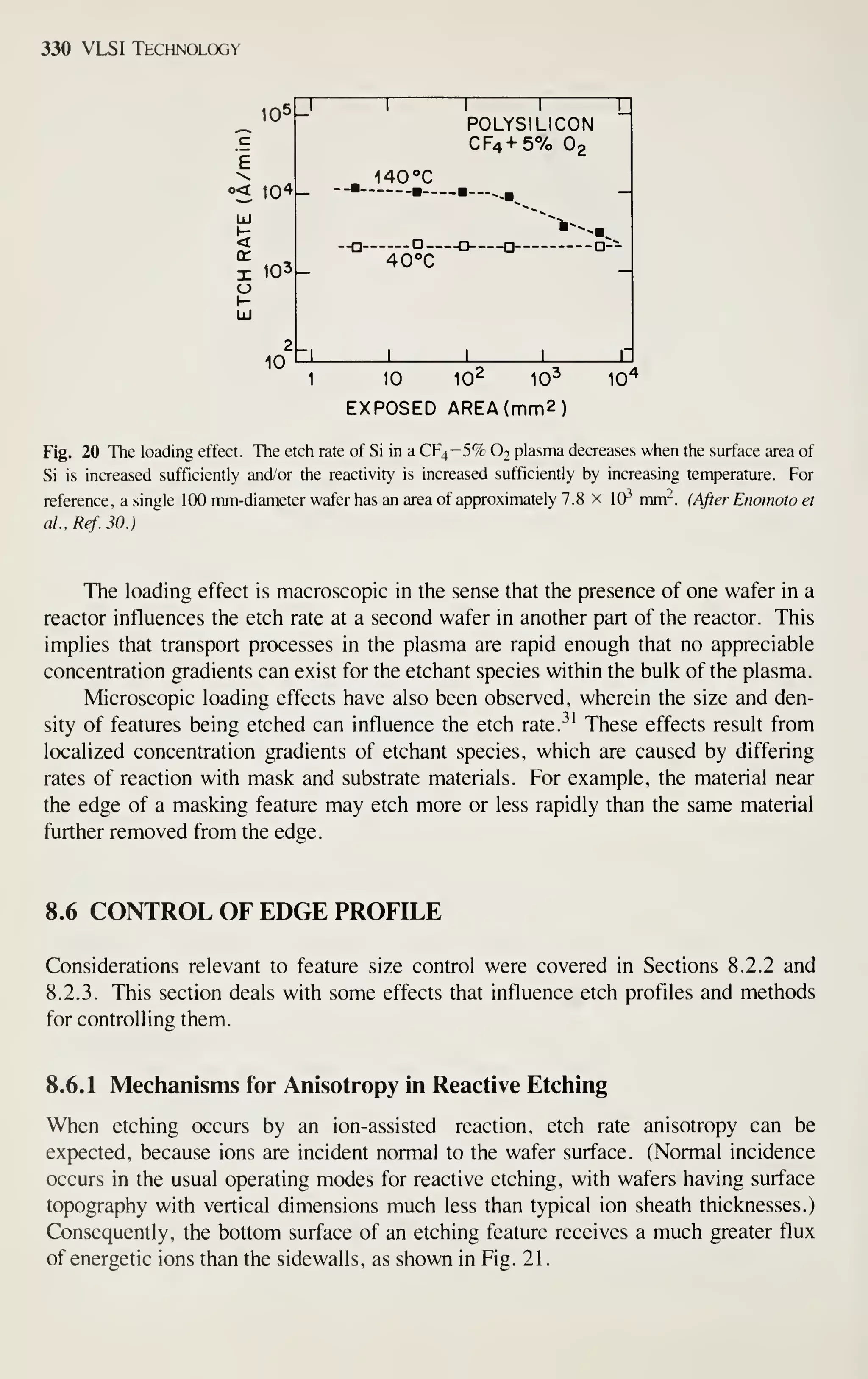
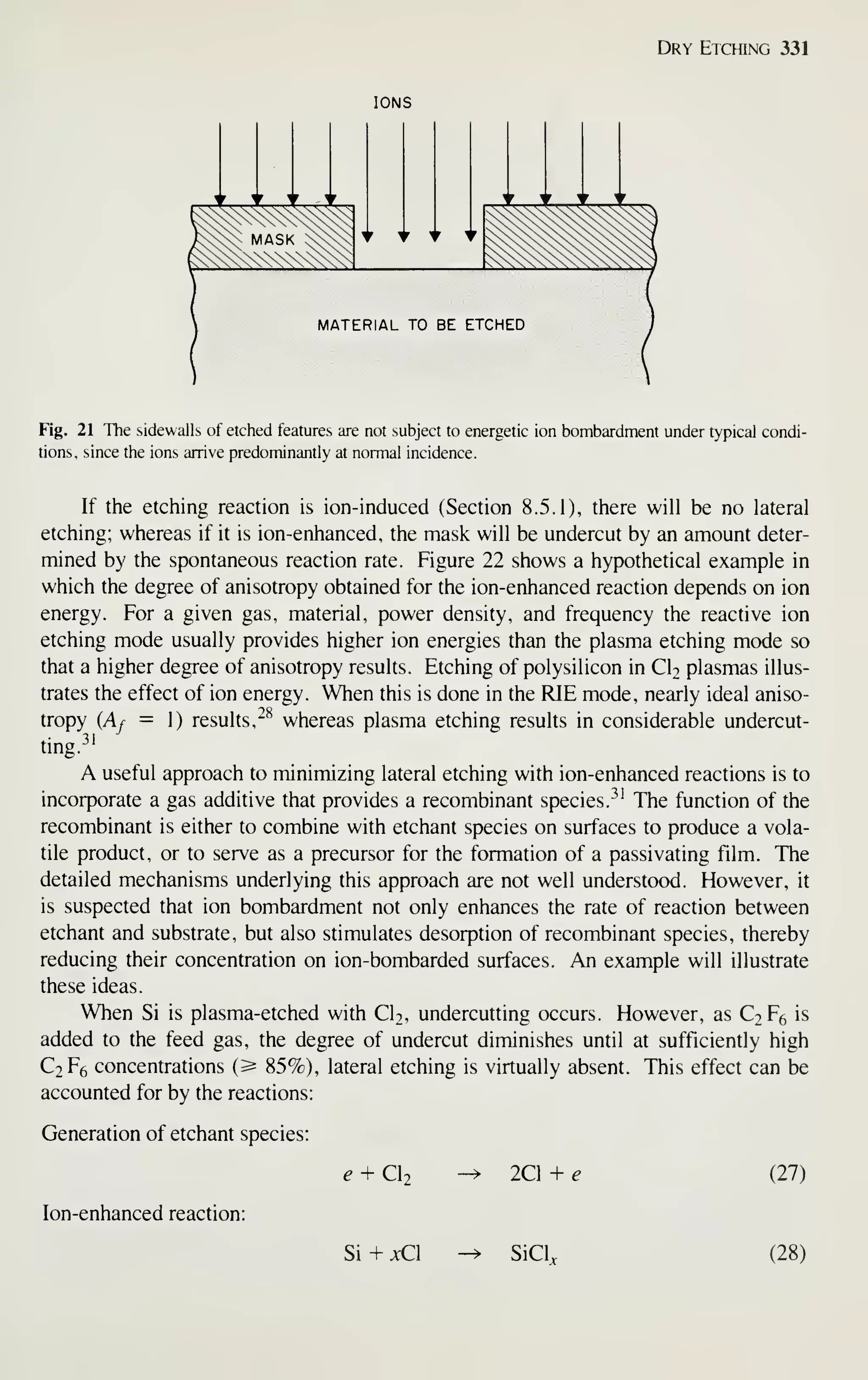
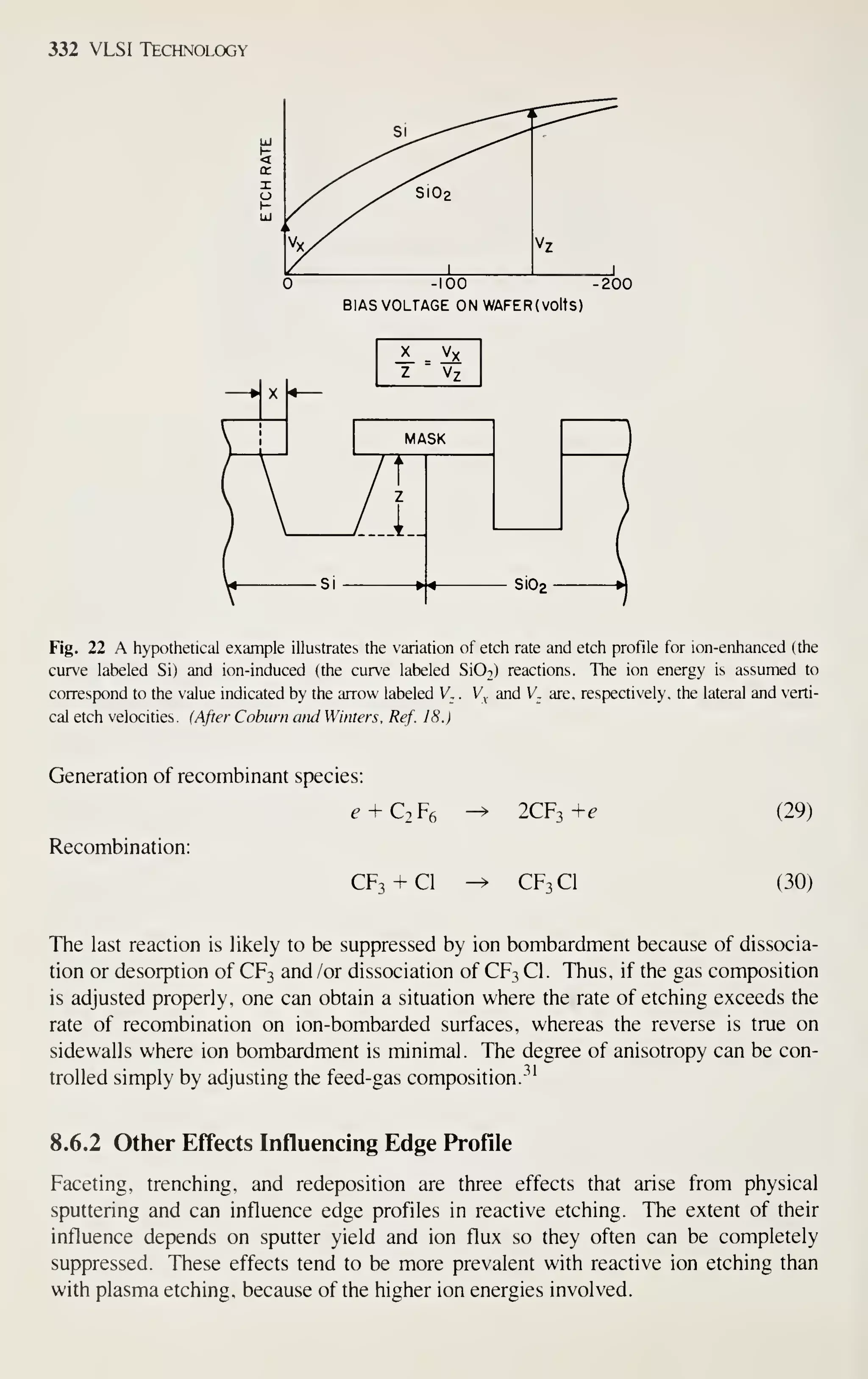
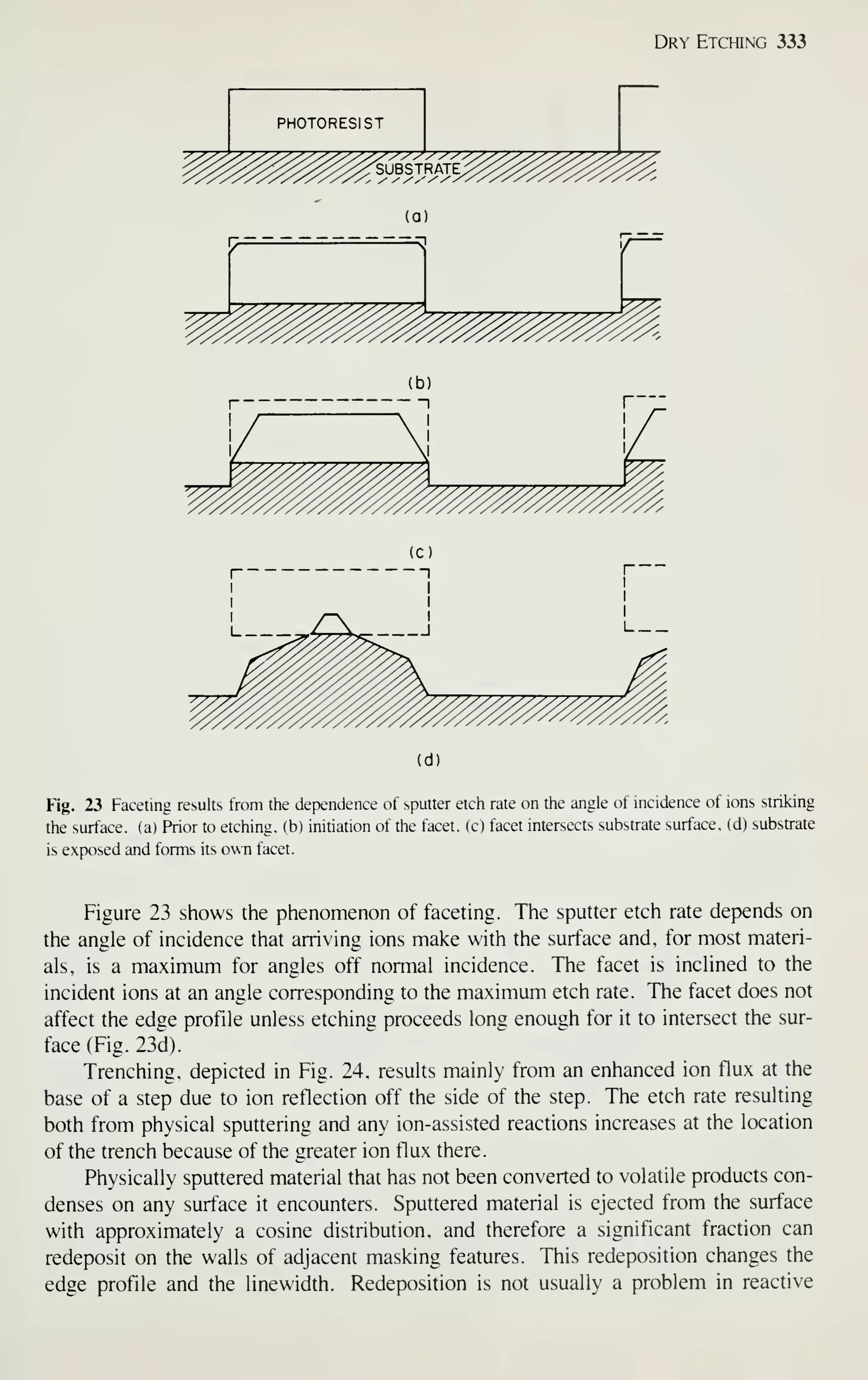
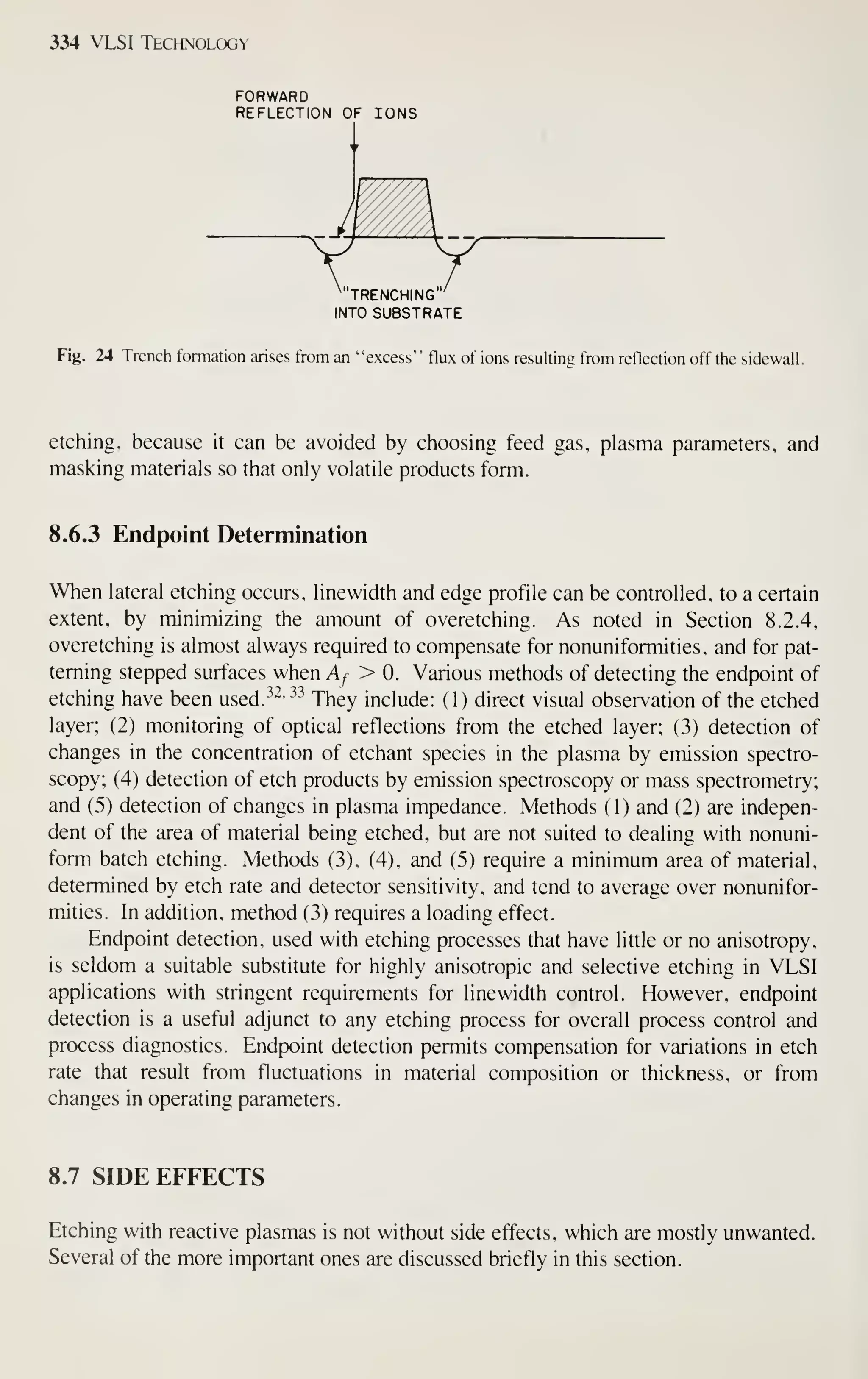
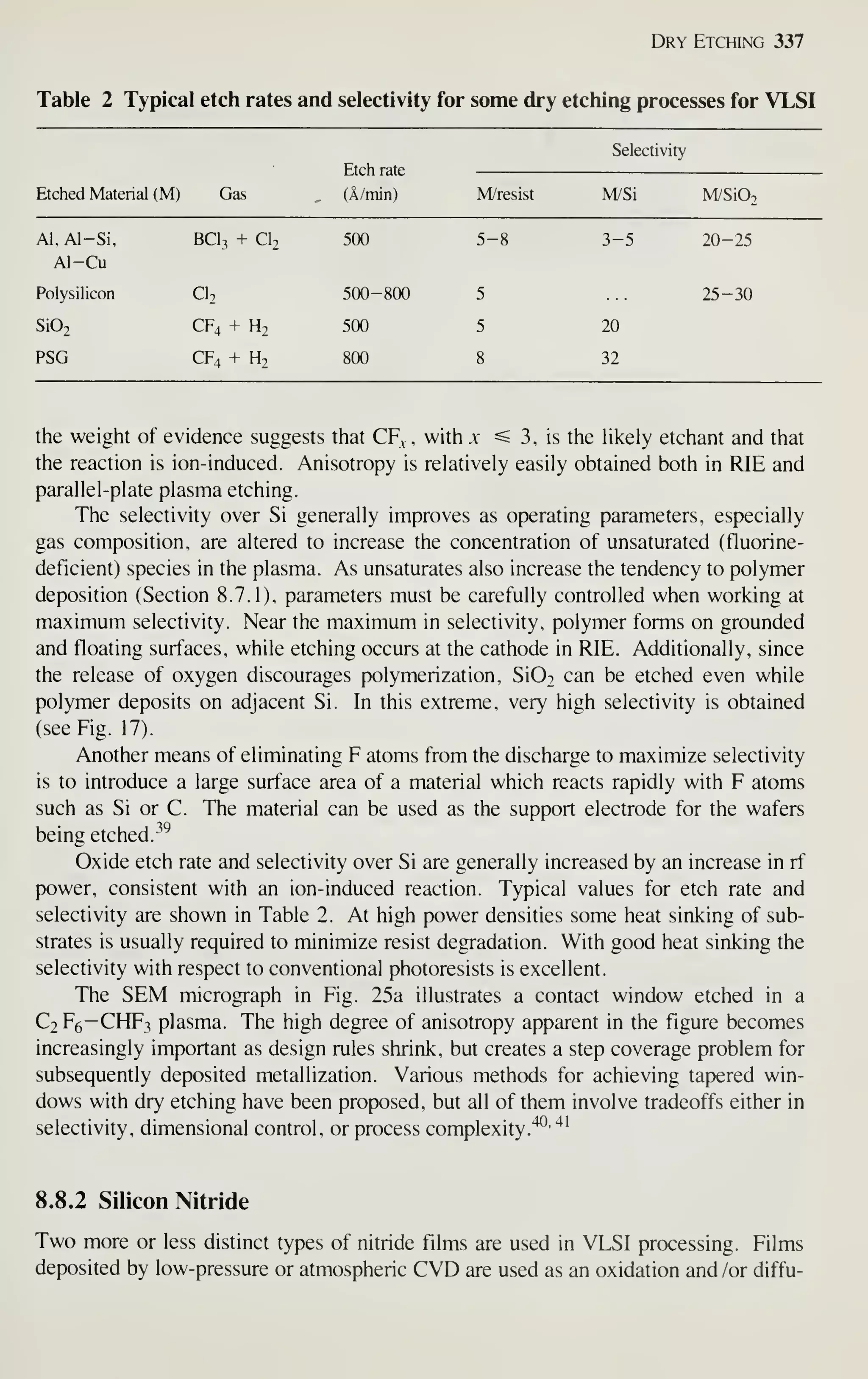
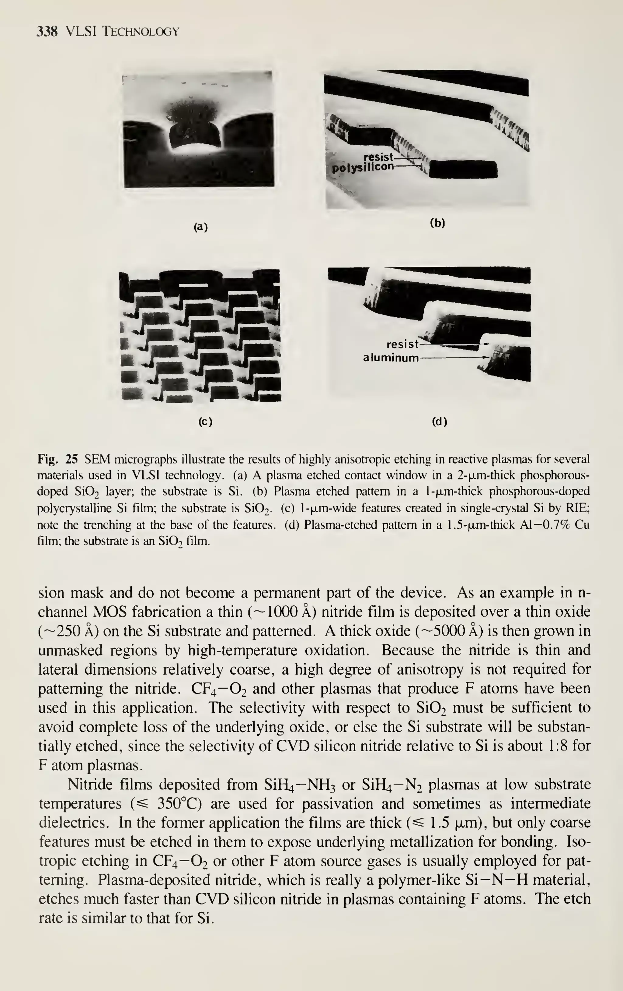
![342 VLSI Technology
Etch rate, selectivity, and anisotropy are determined by various parameters
including gas composition, gas pressure, wafer temperature, and the operating fre-
quency and power density of the plasma. These parameters must be carefully con-
trolled to avoid unwanted effects such as polymer deposition and radiation damage.
Plasma processes have been developed for etching most of the materials used in
VLSI technology. However, improvements in selectivity, edge profile control, repro-
ducibility, overall process control, automation, and throughput are needed.
Better selectivity and profile control will be particularly important to efforts to
further reduce the size of circuit features. Future work will lead to increased etch
rates. Faster etching will shift the focus in dry etching equipment to single- wafer sys-
tems, with cassette to cassette, fully automated wafer processing.
The future will also see dry etching extended to new materials and devices, and
significant advances in our understanding of the complex physics and chemistry
underlying dry etching processes.
REFERENCES
[1] C. M. Melliar-Smith and C. J. Mogab, "Plasma-Assisted Etching Techniques for Pattern Delinea-
tion," in J. L. Vossen and W. Kern. Eds., Thm Film Processes. Academic, New York, 1979.
[2] S. M. Irving, "A Plasma Oxidation Process for Removing Photoresist Films," Solid State Technol.,
14(6), 47 (1971).
[3] S. M. Irving, K. E. Lemons, and G. E. Bobos, "Gas Plasma Vapor Etching Process," U.S. Patent
3,615,956. (Filed March 27, 1969; patented Oct. 26. 1971.)
[4] T. C. Penn, "Forecast of VLSI Processing —A Historical Review of the First Dry-Processed IC",
IEEE Trans. Electron Devices, ED-26, 640 (1979).
[5] D. L. Tolliver, "Plasma Processing in Microelectronics —Past, Present, and Future," Solid State
Technol., 25, 99 (9S0).
[6] G. K. Wehner and G. S. Anderson, "The Nature of Physical Sputtering," in L. I. Maissel and R.
Glang, Eds.. Handbook of Thin Film Technology. McGraw-Hill, New York, 1970.
[7] D. Bollinger and R. Fink, "A New Production Technique; Ion Milling," Solid State Technol.. 25. 79
(1980).
[8] B. Chapman, Glow Discharge Processes. Wiley, New York, 1980.
[9] J. L. Vossen, "Glow Discharge Phenomena in Plasma Etching and Deposition," J. Electrochem.
Soc, 126,319(1979).
[10] H. R. Koenig and L. I. Maissel, "Applications of RF Discharges to Sputtering," IBM J . Res. Dev.,
14, 168(1970).
[11] J. W. Cobum and E. Kay, "Positive-Ion Bombardment of Substrates in RF Diode Glow Discharge
Sputtering," y. Appl. Phys.. 43, 4965 ( 1972).
[12] A. R. Reinberg, "Dry Processing for Fabrication of VLSI Devices," in N. G. Einspruch, Ed.. VLSI
Electronics. Academic, New York, 1981, Vol. 2.
[13] D. B. Eraser et al. Pumping Hazardous Gases. American Vacuum Society. New York, 1980.
[14] R. H. Bruce, "Anisotropy Control in Dry Etching," Solid State Technol.. 24, 64 (1981).
[15] D. F. Downey, W. R. Bottoms, and P. R. Hanley, "Introduction to Reactive Ion Beam Etching,"
Solid State Technol.. 26, 121 (1981).
[16] C. M. Melliar-Smith. "Ion Etching for Pattern Delineation," J. Vac. Sci. Technol.. 13, 1008 (1976).
[17] J. W. Cobum and H. F. Winters, "Ion- and Electron-Assisted Gas-Surface Chemistry —An Important
Effect m Plasma Etching," 7. Appl. Phys., 50, 3189 (1979).
[18] J. W. Cobum and H. F. Winters, "Plasma Etching—A Discussion of Mechanisms," J. Vac. Sci.
Technol., 16,391(1979).](https://image.slidesharecdn.com/simonm-220913174129-44ec6f82/75/Simon-M-Sze-editor-Very-Large-Scale-Integration-VLSI-Technology-McGraw-Hill-Inc-US-1983-pdf-362-2048.jpg)
![344 VLSI Technology
[47] T. P. Chow and A. J. Steckl, "Plasma Etching Characteristics of Sputtered MoSi2 Films," Appl.
PhyS.Lett.. 31. 466 {9m.
[48] E. C. Whitcomb and A. B. Jones, "Reactive Ion Etching of Submicron MoSiT/Poly-Si Gates for
CMOS/SOS Devices," Solid State TechnoL. 25, 121 (1981).
[49] D. W. Hess, "Plasma Etching of Aluminum." Solid State TechnoL. 24, 189 (1981).
[50] W. Y. Lee, J. M. Eldridge, and G. C. Schwartz, "Reactive ion Etching Induced Corrosion of Al and
Al-Cu Films," y. Appl. Phys., 52, 2994 (1981).
PROBLEMS
1 Assuming a mask that cannot erode, sketch the edge profile of an isotropically etched feature in a film of
thickness hj on an unetchable substrate for (a) etching just to completion, ib) 100% overetch, and (f ) 200%
overetch. What shape does the profile tend toward as overetching proceeds? Comment on the advisability
of estimating the degree of anisotropy of etching from scanning electron micrographs of edge profiles taken
after removal of the masking layer.
2 By tracing the trajectory during etching of a point on the beveled edge of the mask in Fig. 5, arrive at
Eq. 7.
3 Show that Eq. 12 results when the thinnest and fastest etching portion of the film is assumed to be over
the fastest etching portion of the substrate.
4 Polysilicon lines 0.5 ixm thick pass over a field oxide step 1 . 1 [xm high and across a gate oxide 0.05 iJim
thick. Calculate the selectivities required with respect to mask and gate oxide if the polysilicon is etched
with a process having 10% etch rate uniformity, Af = 1 .0, and A,„ = 0.5. Assume 5% polysilicon thick-
ness uniformity, 5% mask etch rate uniformity, a mask edge profile of 60°, and that linewidth must be con-
trolled to 0.2 |jLm.
5 Consider a discharge in CF4. Assume that electrons and gas molecules can be treated as hard spheres with
masses m and M, respectively. Calculate the maximum fractional loss of kinetic energy for an electron strik-
ing a CF4 molecule. Consider the CF4 molecule initially at rest, and the collision to be elastic. Repeat the
calculation for an inelastic collision where the potential energy of the CF4 molecule increases by the max-
imum amount possible.
6 A CF4—Ot rf plasma is operated at 300 W, and 0.5 torr, with a feed-gas flow rate of 100 cm- /min (STP).
The plasma occupies a volume of 4000 cm^^. Under these conditions atomic fluorine is generated at a rate of
10'^ cm"^ — s~' in the plasma. The combined effect of loss mechanisms for F atoms results in a rate of
loss proportional to the F atom concentration. In steady state, this concentration is measured as
3 X lO'^cm"^. What is the mean lifetime of F atoms for these conditions? How does it compare to the
residence time of an average molecule in the plasma? How would the etch rate of Si be affected if the flow
rate were increased tenfold while holding other parameters constant?
7 What is the function of the ground shield shown in Fig. 11? What limitation is there on the spacing
between the ground shield and the powered electrode?
8 What are the major distinctions between reactive ion etching and parallel-plate plasma etching? Compare
the advantages and limitations of these techniques.
9 Would you expect the rate of an ion-assisted reaction between neutral species and a solid surface to be
independent of the angle of incidence of the ion beam? Why? What do you expect would happen to the
reaction rate as the ion energy was increased continuously beyond 5 keV?
10 The enthalpy of the exothermic reaction
Si + 4F ^ SiF4
is 370 kcal/g-mole at 25°C. At what rate is heat generated when a 100-mm-diameter, 0.5-mm-thick Si wafer
is etched on one face at a rate of 1 .0 p-m/min in an F generating plasma? Suppose that the wafer is thermally
isolated during etching. By how much will its temperature rise if 5.0 jxm are etched away?](https://image.slidesharecdn.com/simonm-220913174129-44ec6f82/75/Simon-M-Sze-editor-Very-Large-Scale-Integration-VLSI-Technology-McGraw-Hill-Inc-US-1983-pdf-364-2048.jpg)


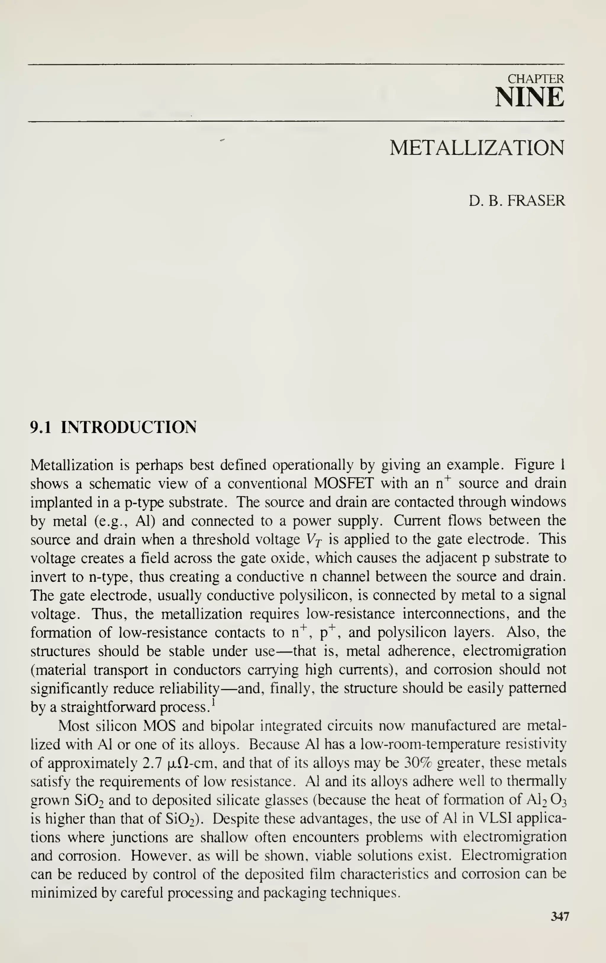
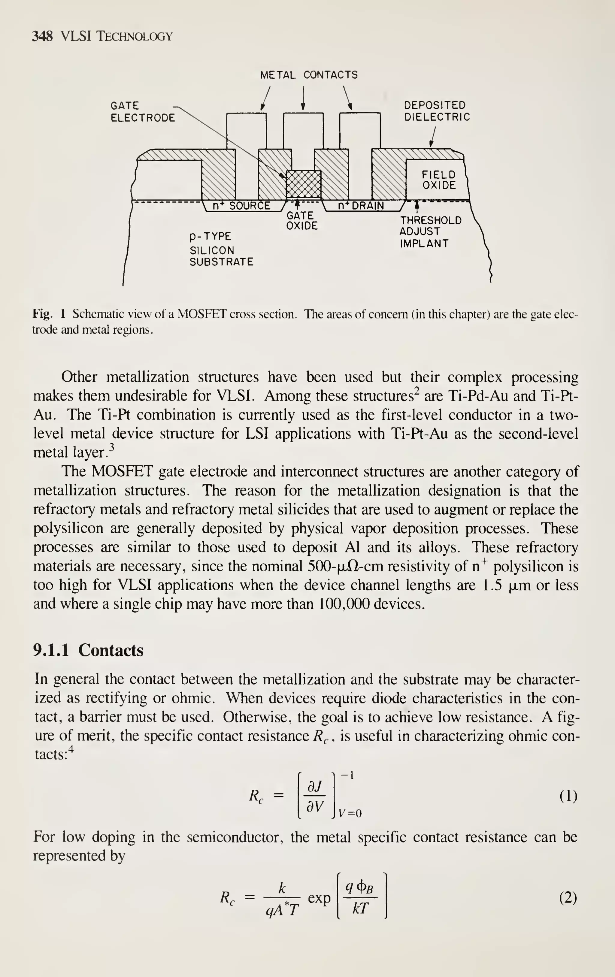
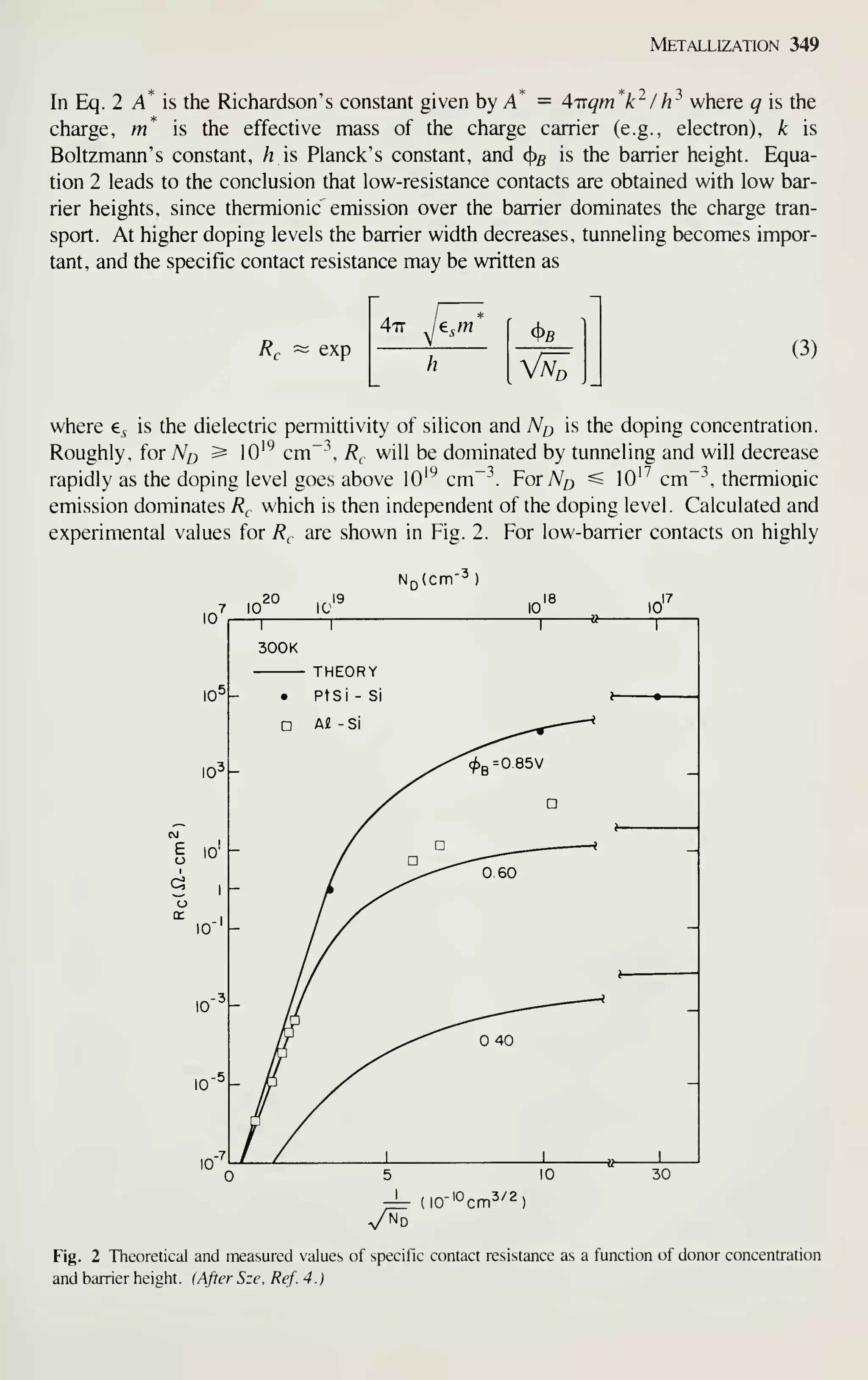
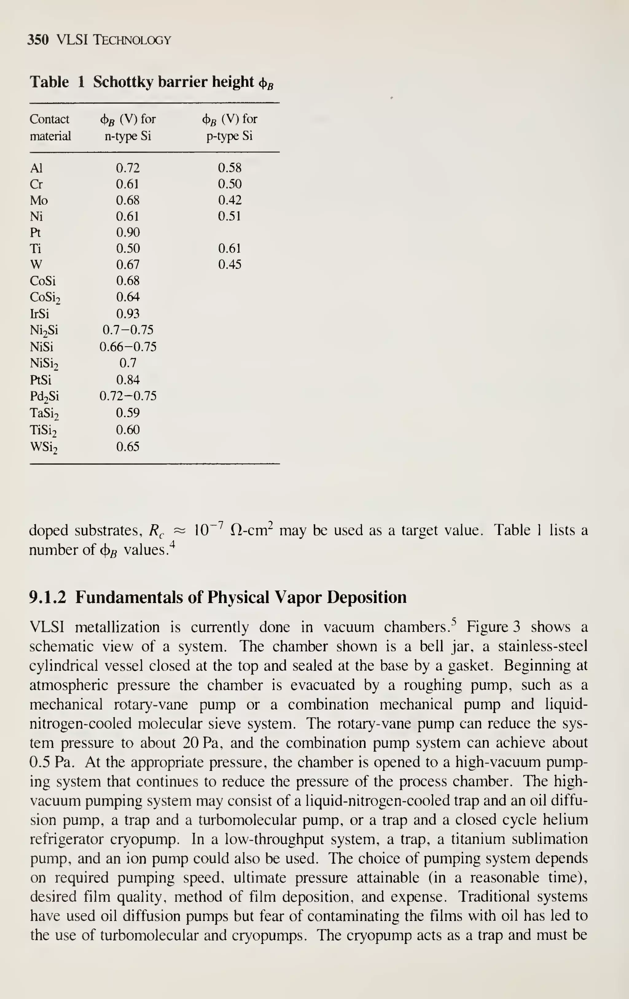
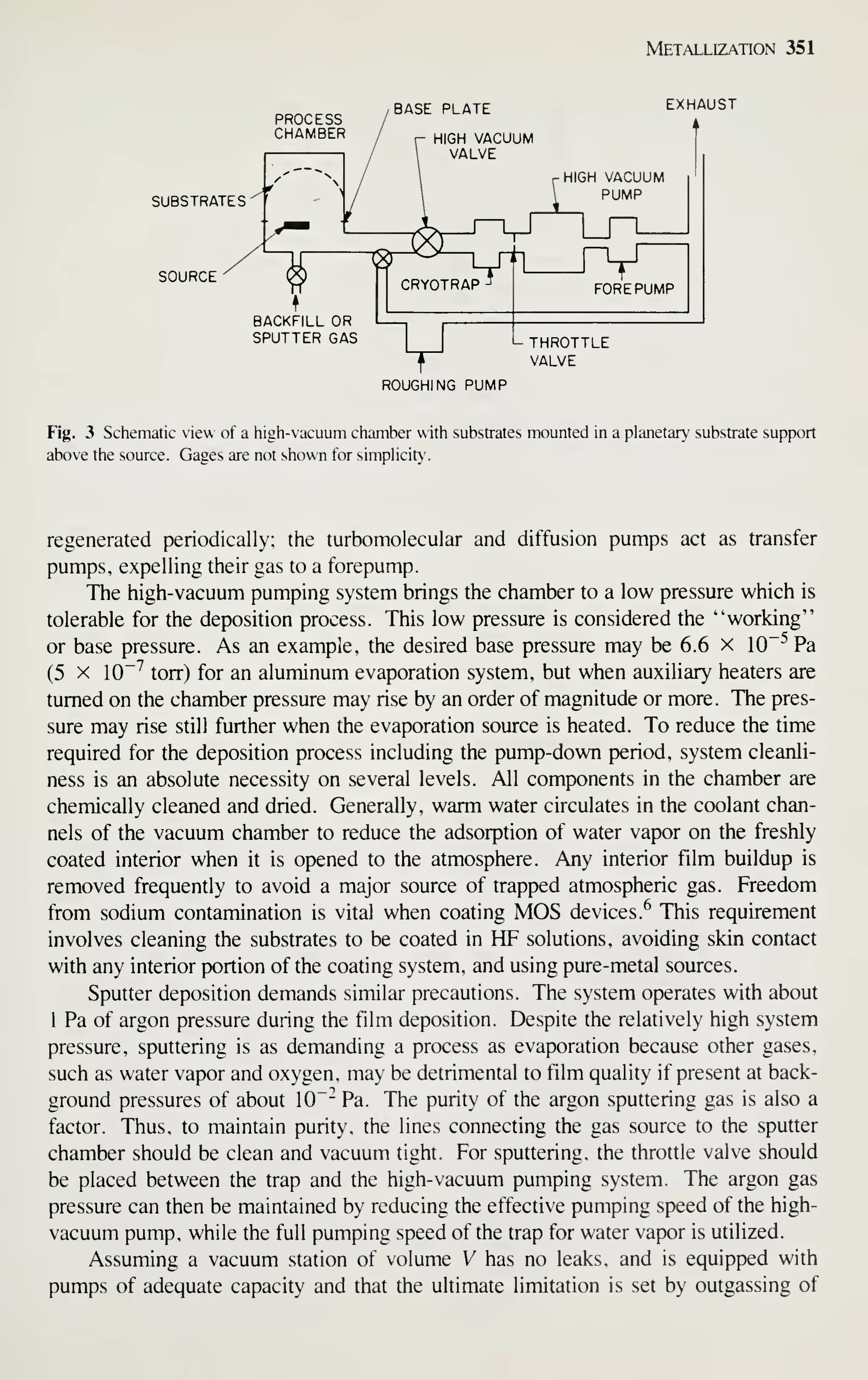
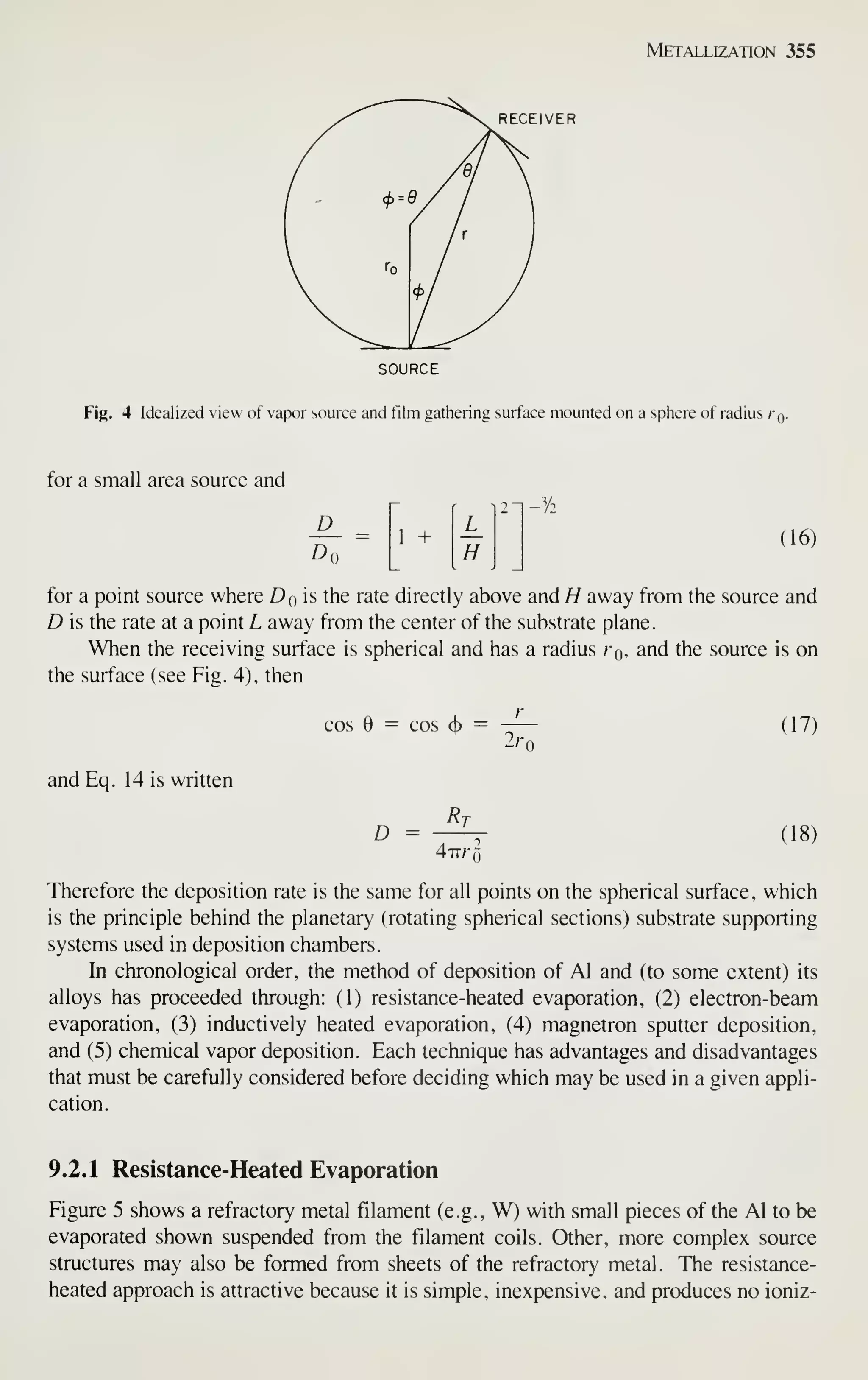
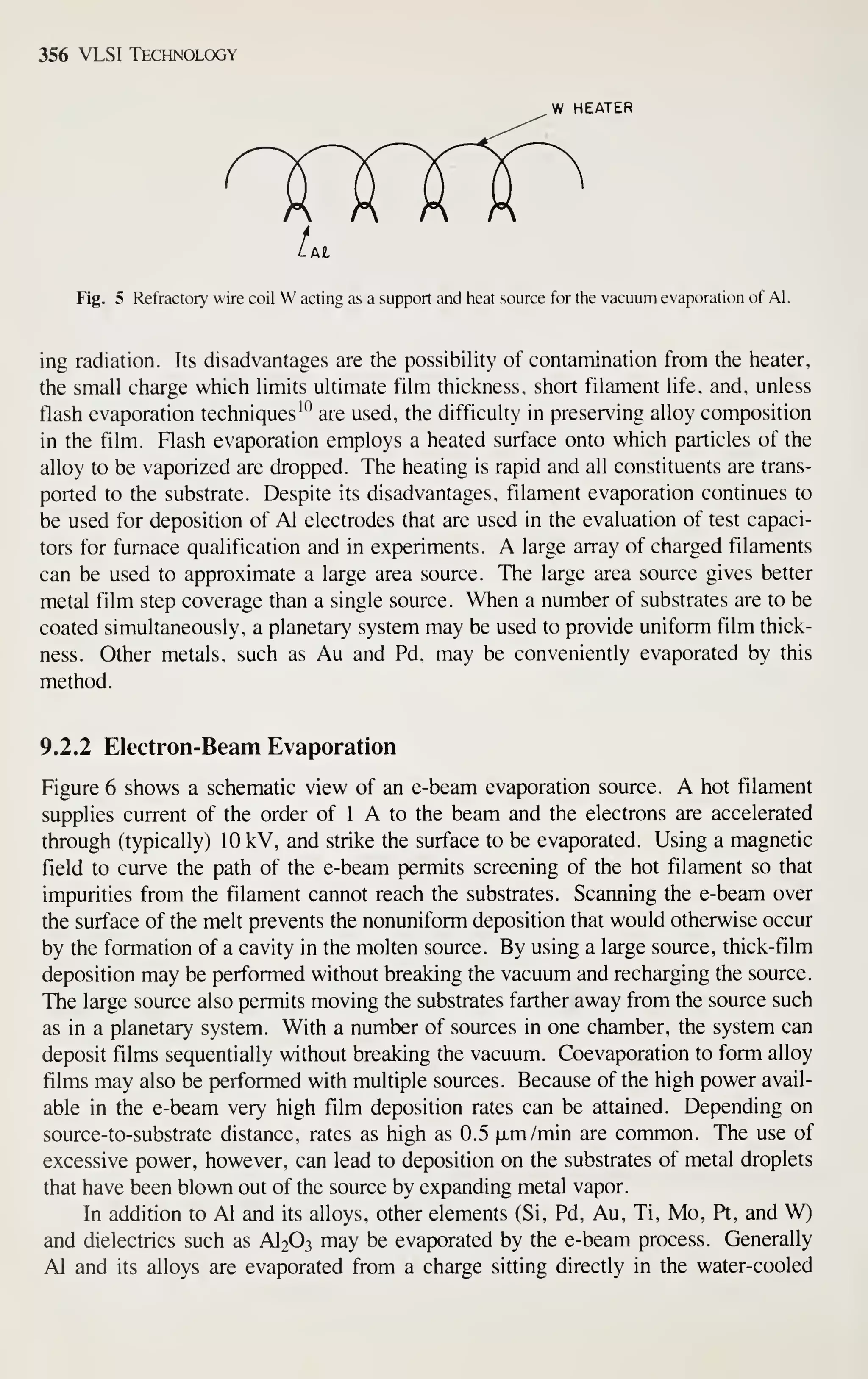
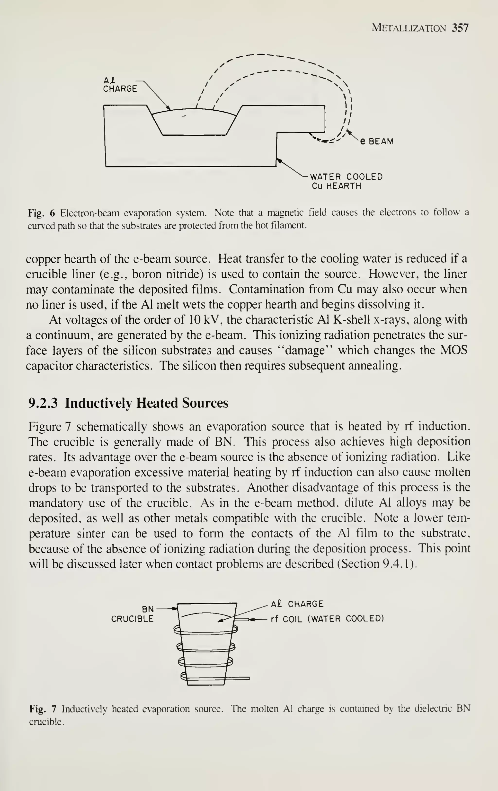
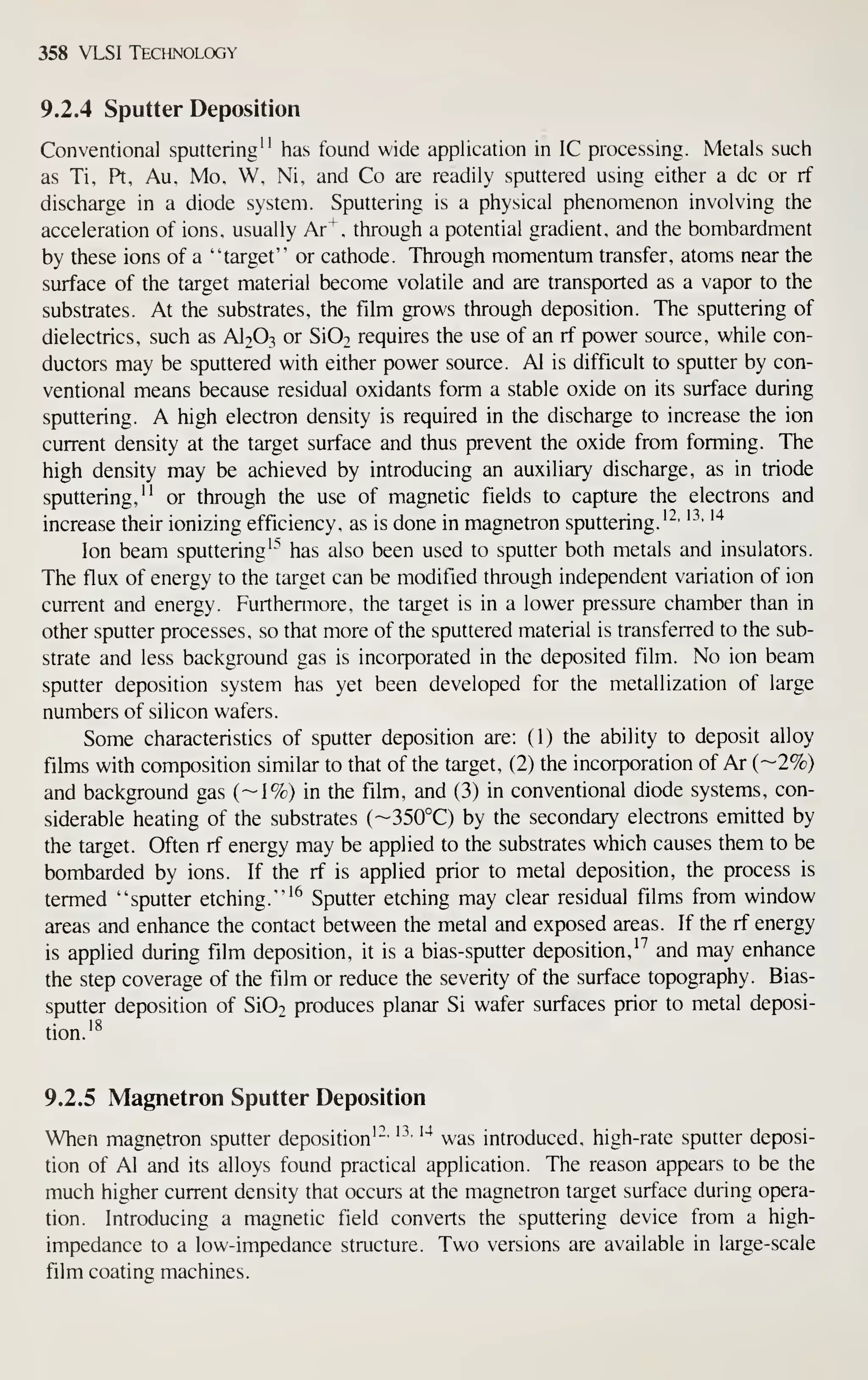
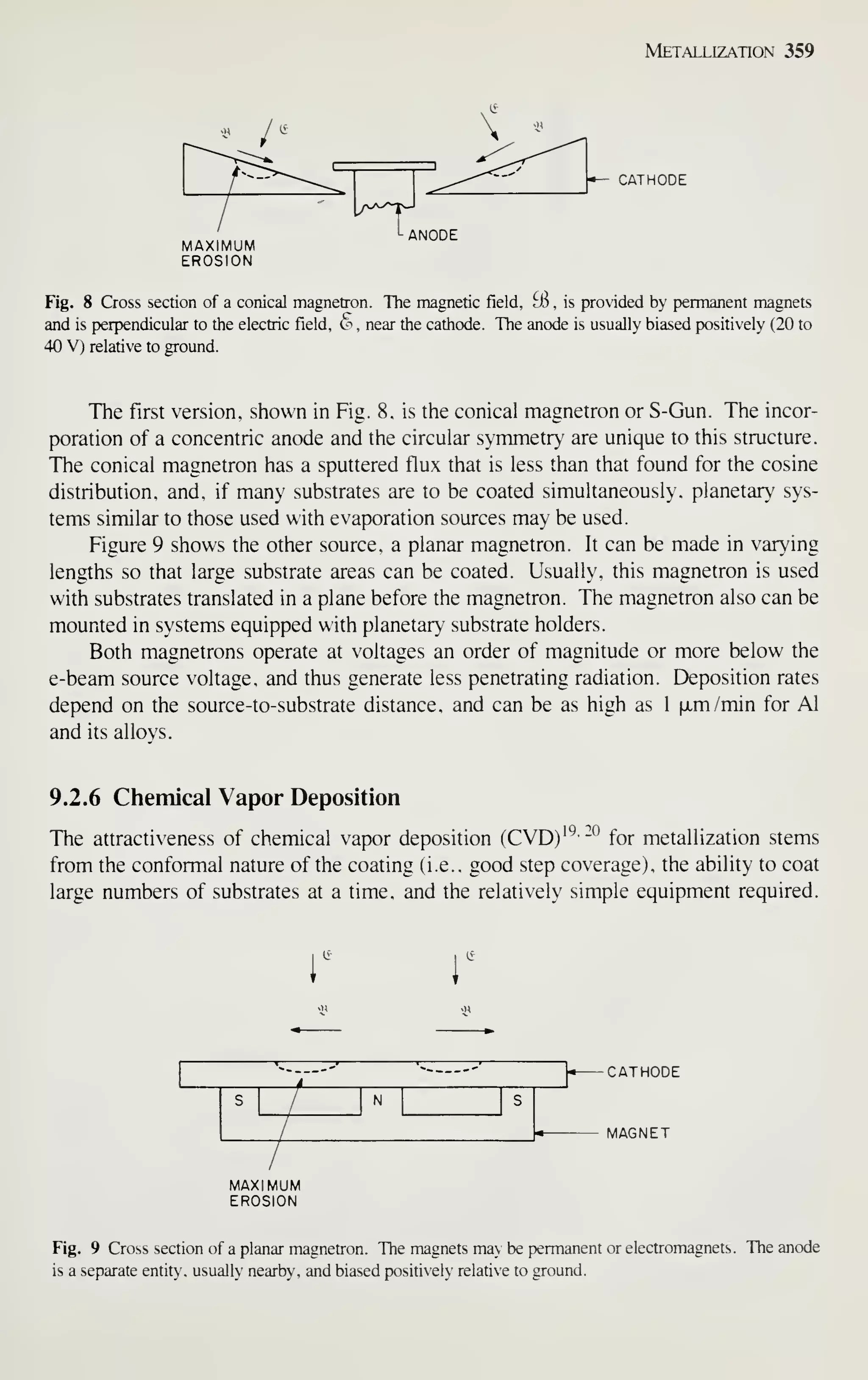
![360 VLSI Technology
Unlike physical vapor deposition, which suffers from shadowing effects and imper-
fect step coverage, low-pressure CVD can yield conformal film coverage over a wide
range of step profiles, and often yields lower bulk electrical resistivity.
The major effort in depositing metal for ICs by CVD has been in W deposition.
Processes for W deposition have been developed with preferential deposition on sili-
con but not oxide. '^'
The W is attractive because of its low electrical resistivity (5.3
ixll-cm) and its refractory nature. Both pyrolytic and reduction reactions have been
used. For example, WF6 may produce W films by:
WF6 + thermal energy ^ W + 3F2 (19)
or
WFe + 3H2 -> W + 6HF (20)
or
WFg + plasma or optical energy -^ W -I- 3F2 (21)
Temperatures may range from 60 to 800°C in the various reactors. The use of WF^
may cause loss of oxide during deposition, and WCl6 may find application where the
fluoride is not suitable, although the chloride requires higher temperatures.
Figure 10 shows a schematic view of a CVD reactor. The reactor tube is sur-
rounded by a furnace and is considered a "hot wall" system. Using rf induction heat-
ing of a susceptor on which the substrates are positioned and cooling the reactor
vessel walls constitutes a "cold wall" system. Arguments for either system have
been based on efficiency of gas usage and particulate contamination.
In addition to W, other metals such as Mo, Ta, Ti, and Al are of interest for
VLSI applications. Reactions such as^^
800°C
2M0CI5 + 5H2 -^ 2Mo + lOHCl (22)
600°C
2TaCl5 + 5H2 -^ 2Ta + lOHCl (23)
600°C
2TiCl5 + 5H2 -^ 2Ti + lOHCl (24)
and using metal organic compounds such as tri-isobutyl aluminum
150°C
[(CH3)2CH-CH2]3A1 -> t(CH3)2CH-CH2]2AlH
+ (CH3)2C=CH2 (25)
followed by
250°C
[(CH3)2CH-CH2]2A1H ^ Al + hUj
+ 2(CH3)2C=CH2 (26)](https://image.slidesharecdn.com/simonm-220913174129-44ec6f82/75/Simon-M-Sze-editor-Very-Large-Scale-Integration-VLSI-Technology-McGraw-Hill-Inc-US-1983-pdf-380-2048.jpg)
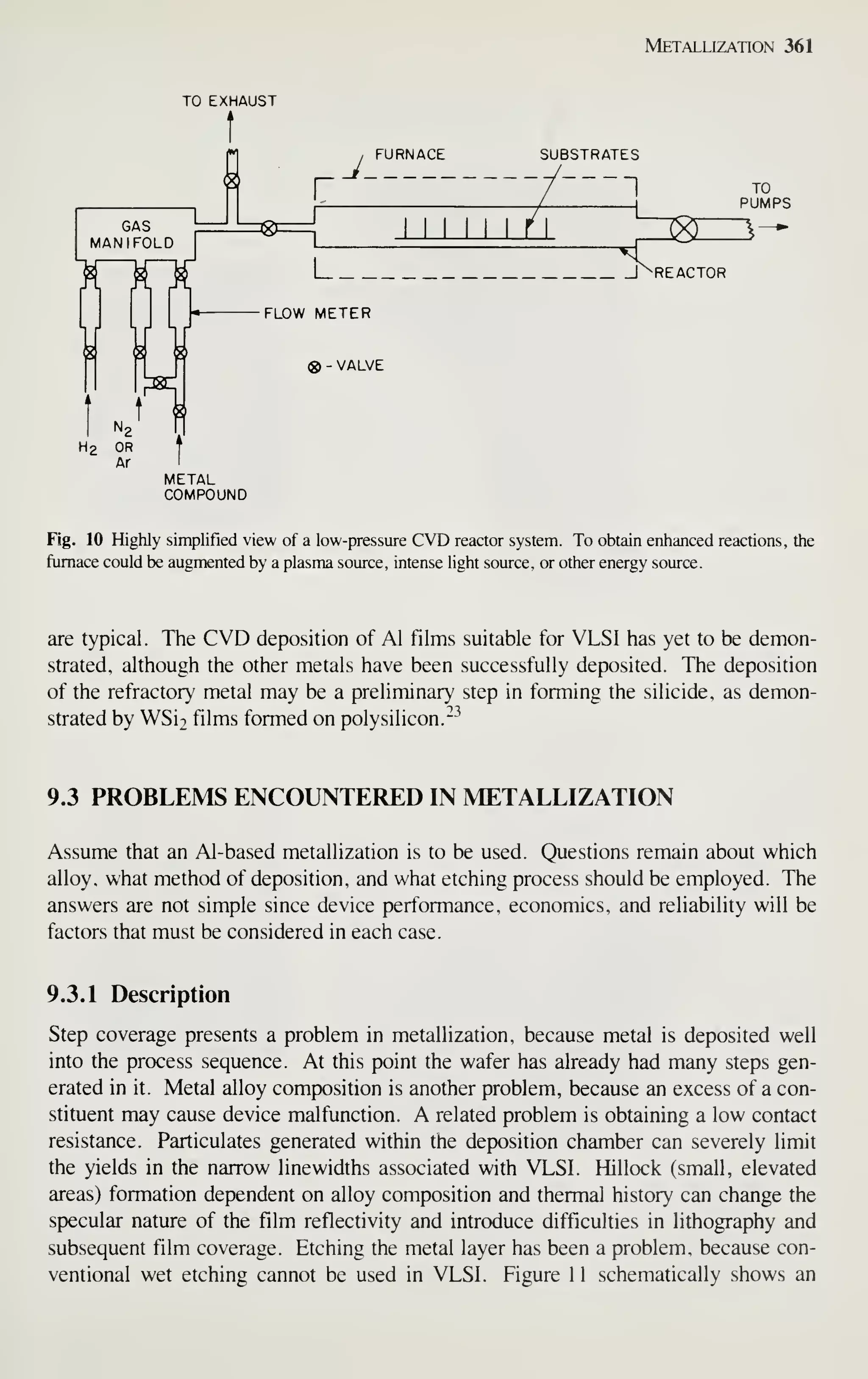
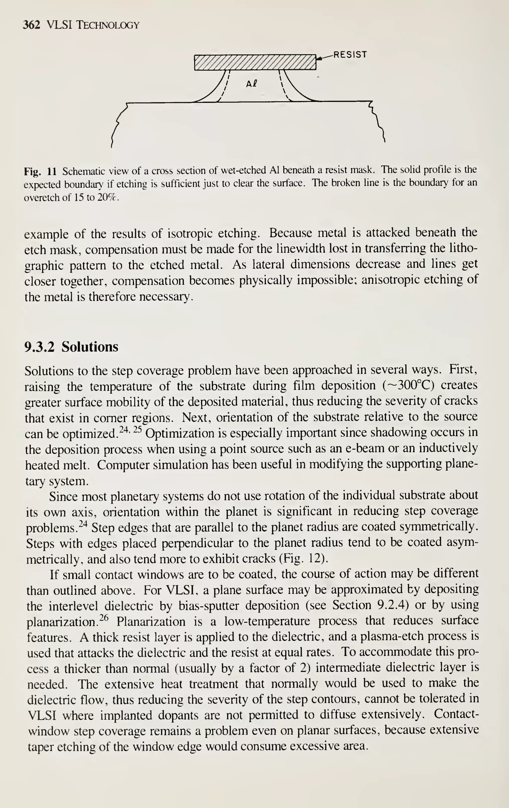
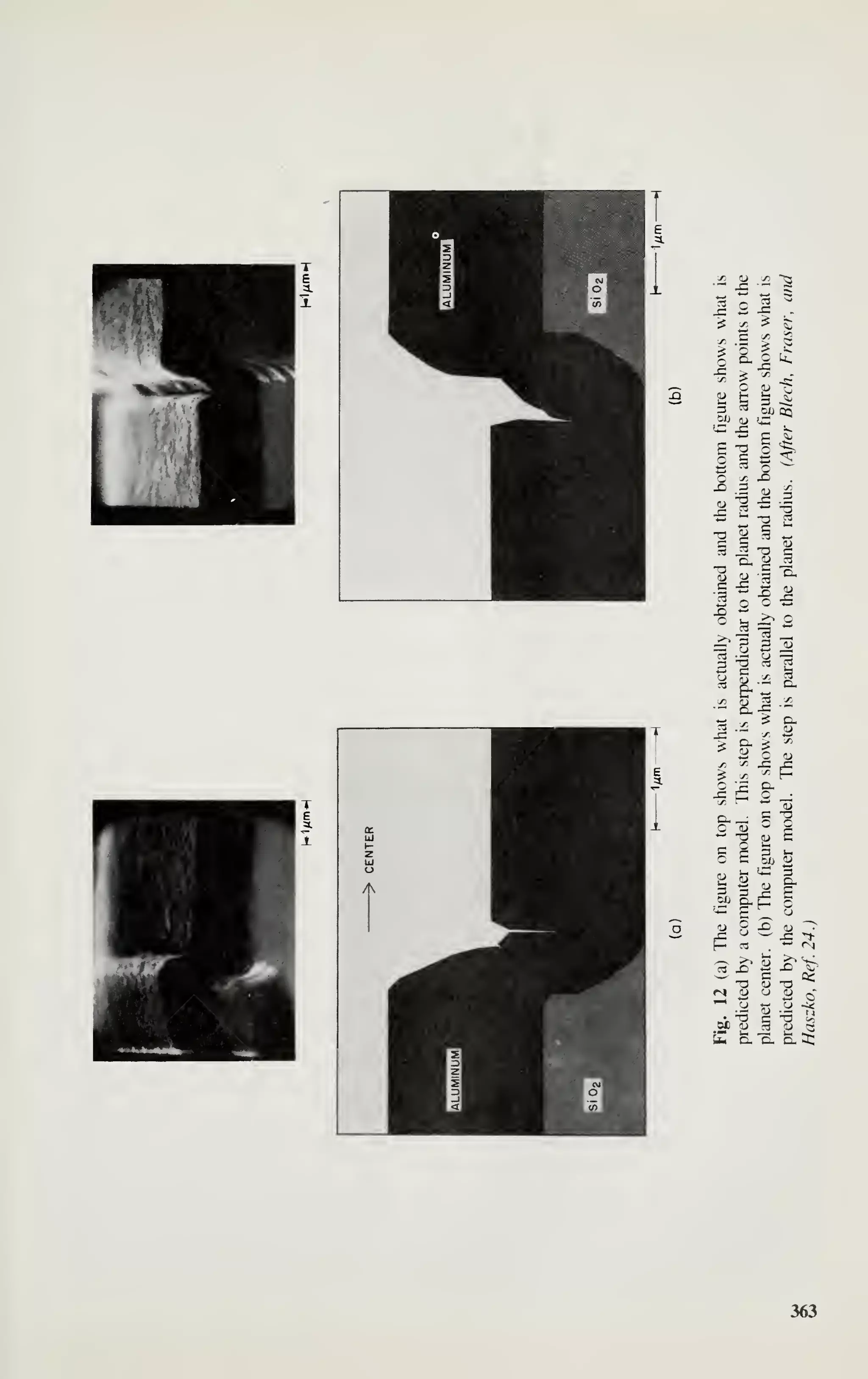
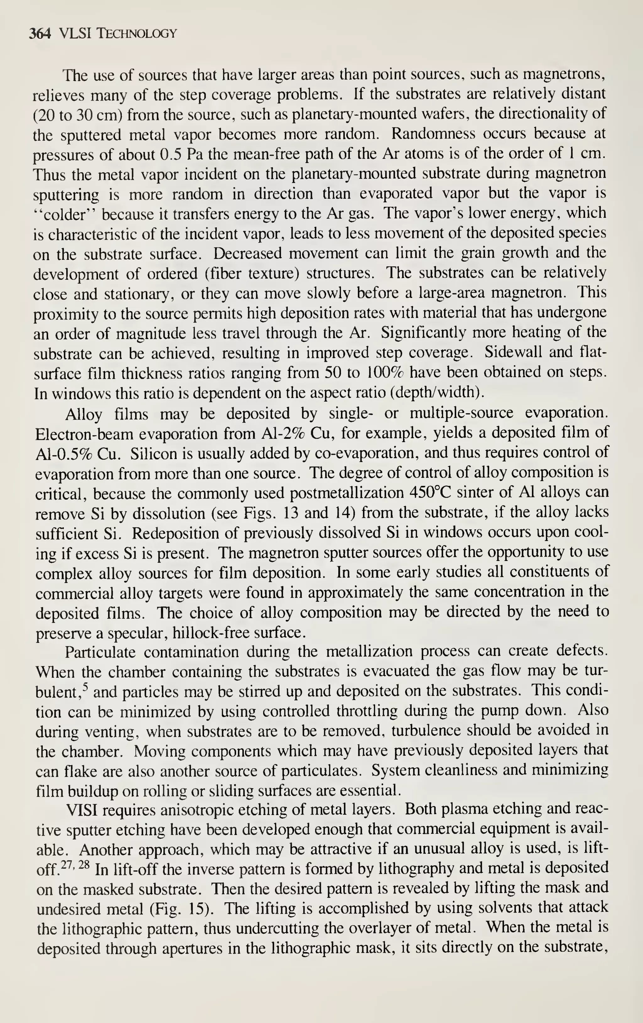
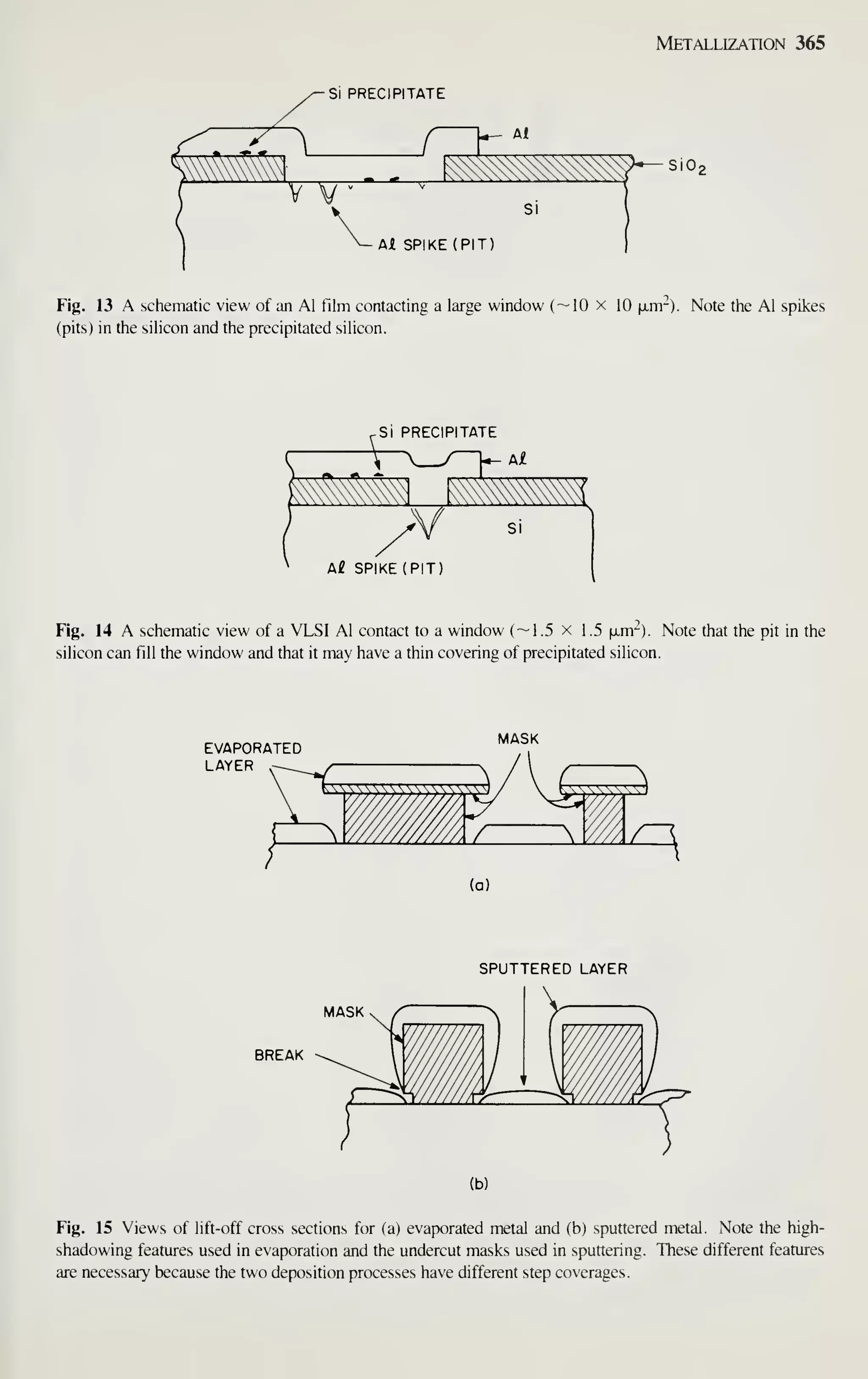
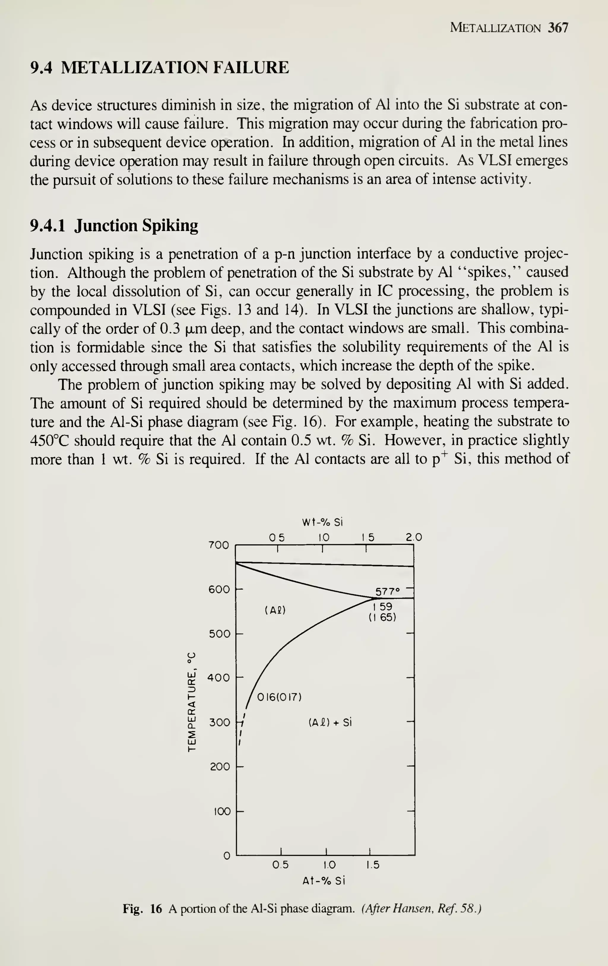
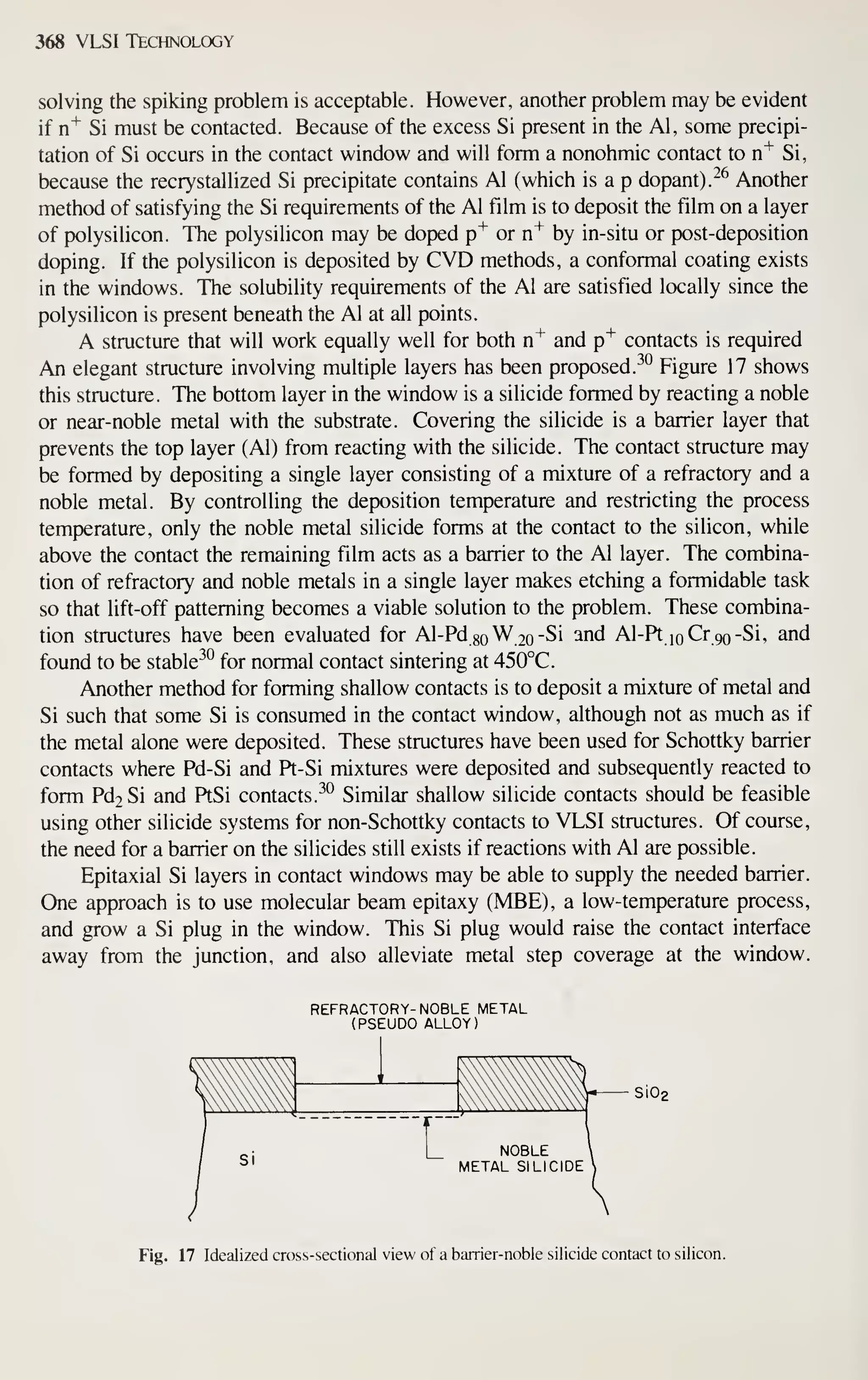
![370 VLSI Technology
(3) (b)
Fig. 18 SEM micrographs of electromigration failure, (a) S-Gun magnetron-deposited Al-0.5 wt. % Cu
and (b) In-Source-evaporated Al-0.5 wt. % Cu. (After Vaidya, Fraser, aiidSinha, Ref. 36.)
view (a) catastrophic melting and balling of the Al is evident. View (b) shows the
area after etching the Al to reveal the polysilicon runners and the Si precipitates. The
arrows indicate the direction of the electron flow.
Electromigration resistance of Al film conductors can be increased by several
techniques. These techniques include alloying with Cu, incorporation of discrete
layers such as Ti, encapsulating the conductor in a dielectric, or incorporating oxygen
during film deposition. ^^ The mean-time-to-failure (MTF) of the conductor can be
related to the current density J in the conductor and an activation energy Q by
MTF ^ J'^ Qxp[Q/kT] (28)
for 10-^ ^ y ^ 2 X 10^ (A/cm-). Experimentally, a value of Q -- 0.5 eV is
obtained, and taken to indicate that low-temperature grain boundary diffusion is the
5 Aim
Fig. 19 SEM view of an electromigration failure of e-beam-evaporated Al on polysilicon. (a) Metal is on
the polysilicon. (b) Al is etched to reveal the polysilicon (After Vaidya. Fraser. andSinlm. Ref. 36.)](https://image.slidesharecdn.com/simonm-220913174129-44ec6f82/75/Simon-M-Sze-editor-Very-Large-Scale-Integration-VLSI-Technology-McGraw-Hill-Inc-US-1983-pdf-390-2048.jpg)
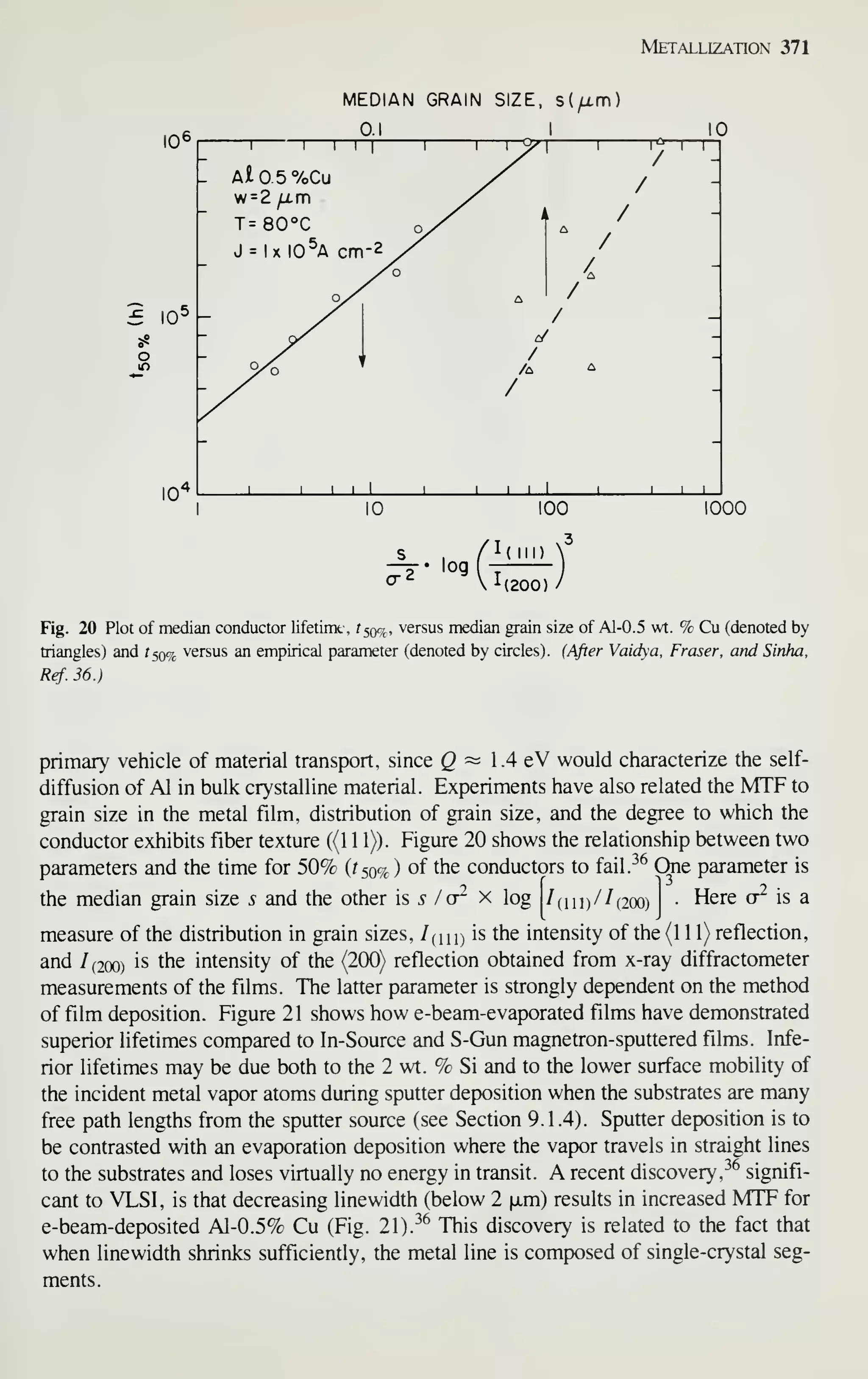
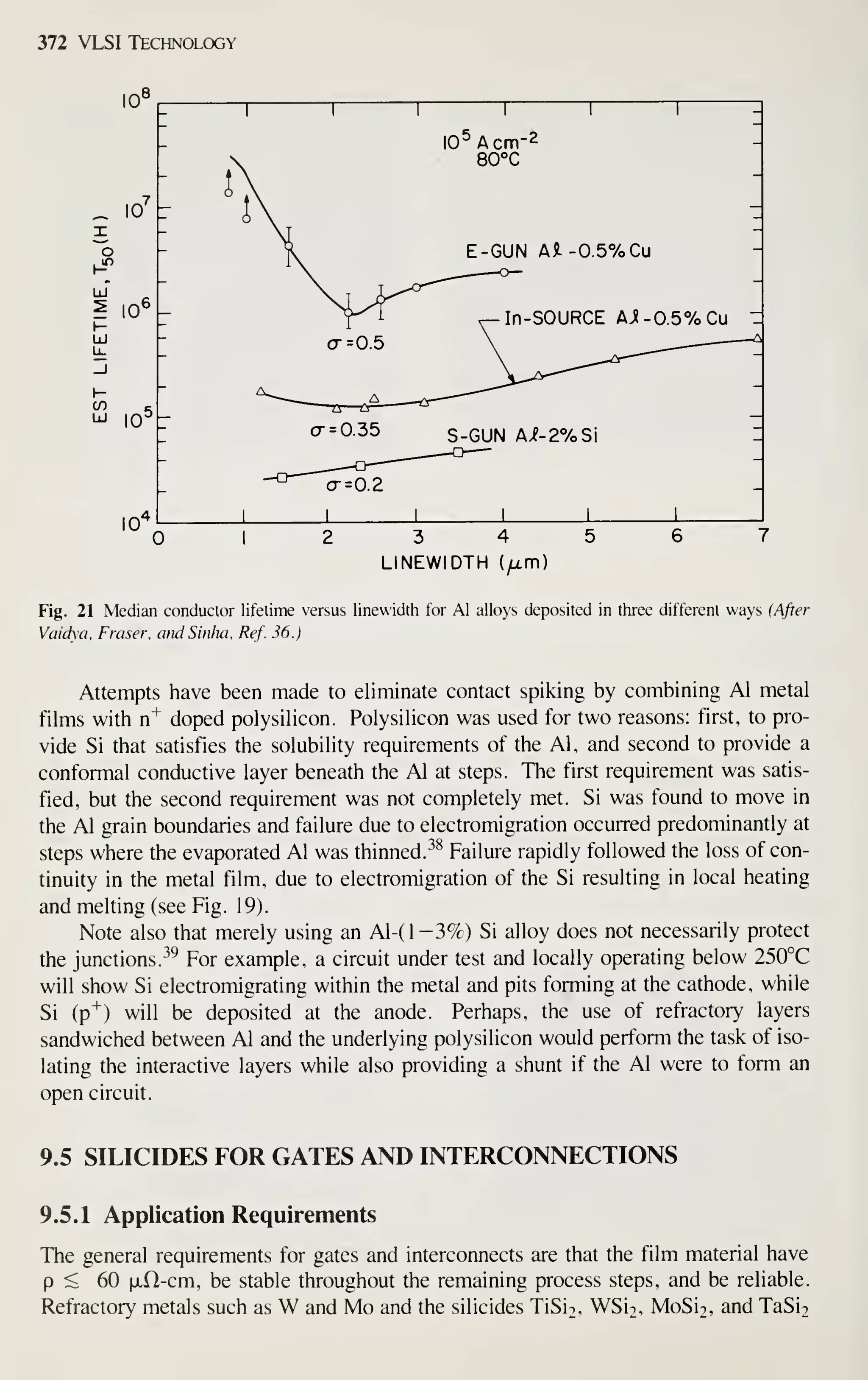
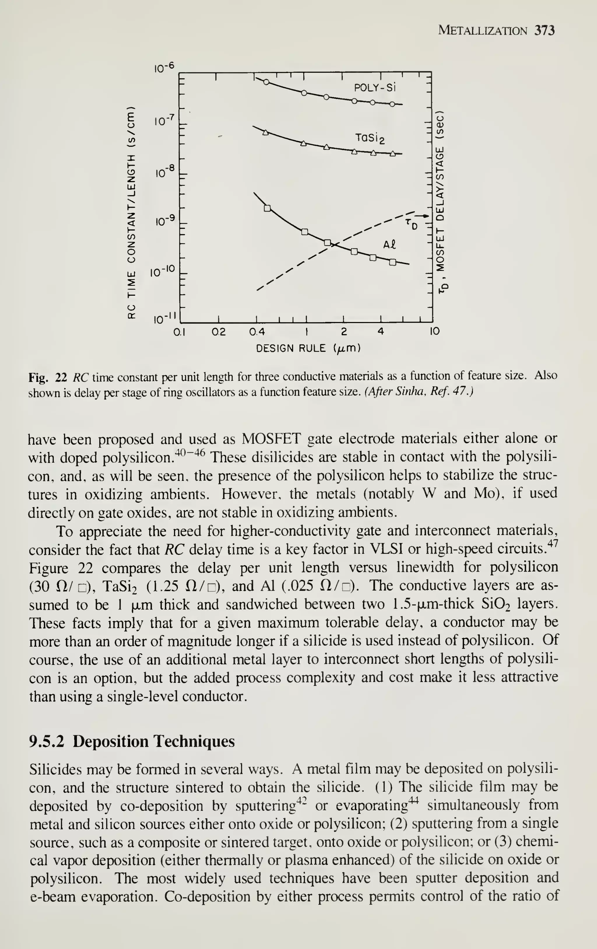
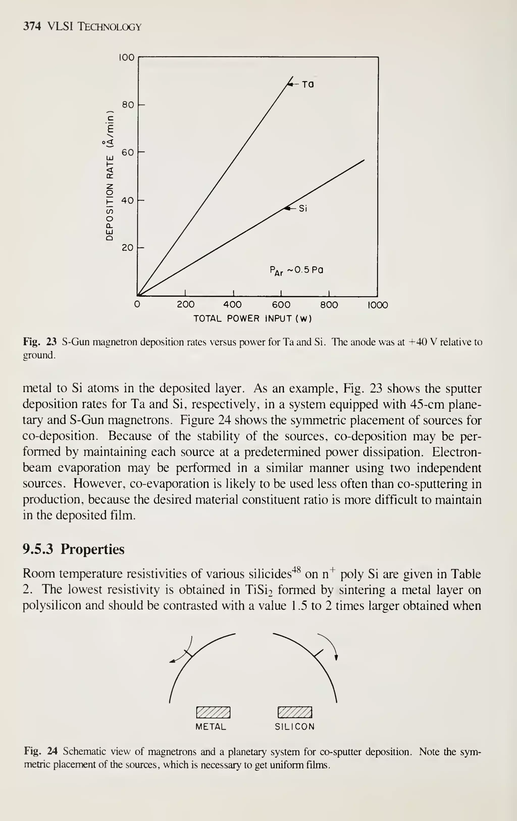
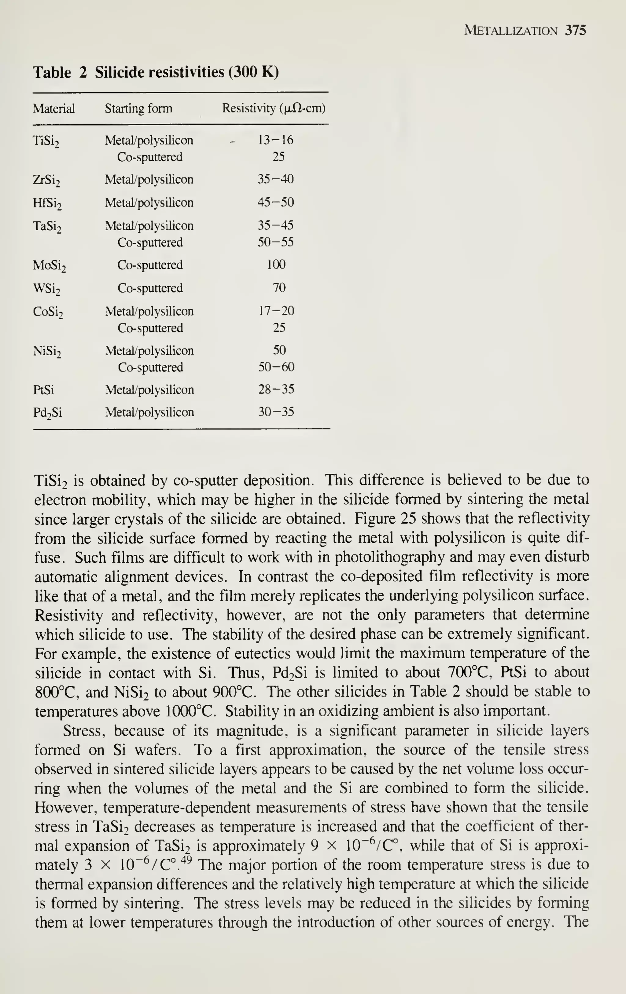
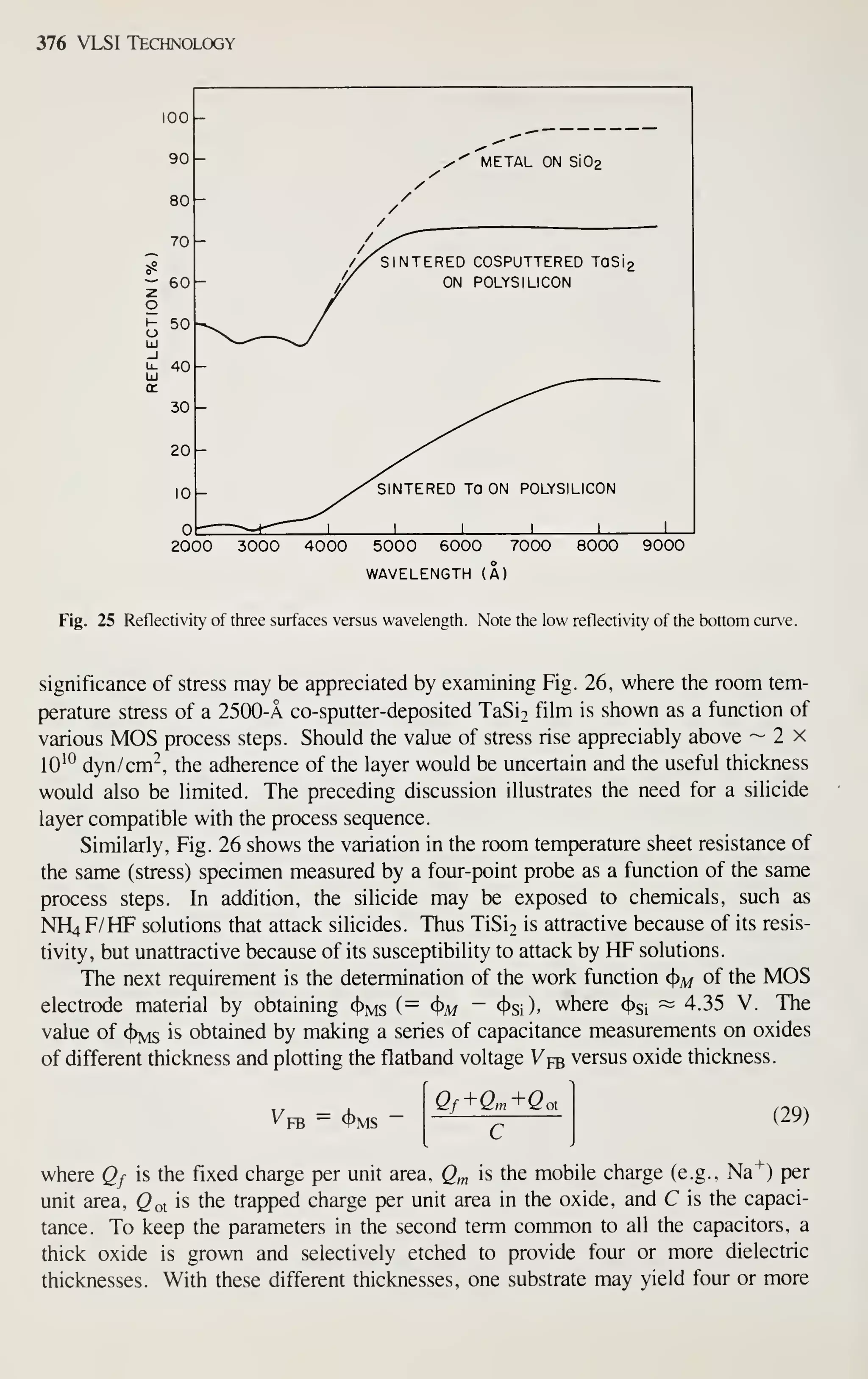
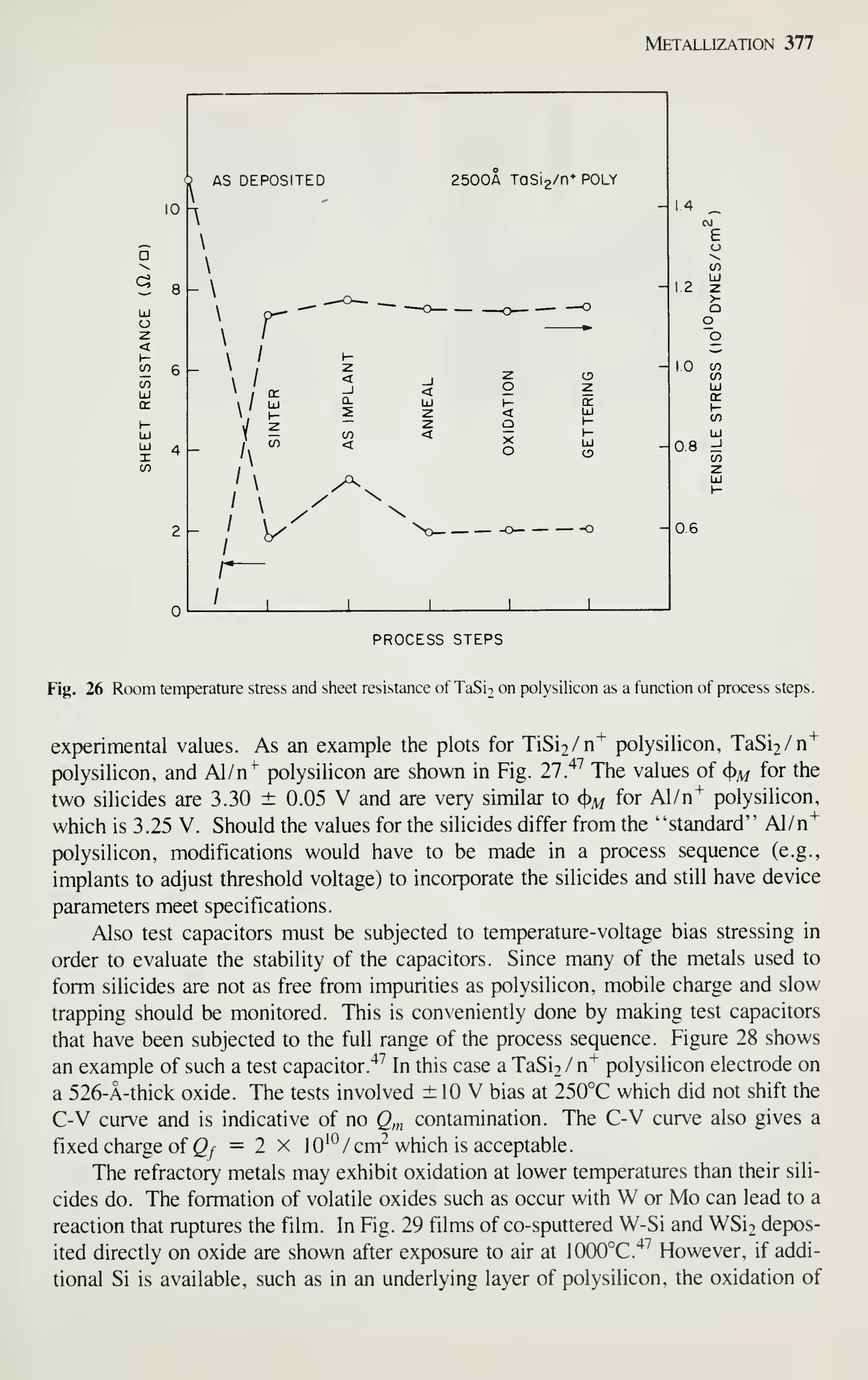
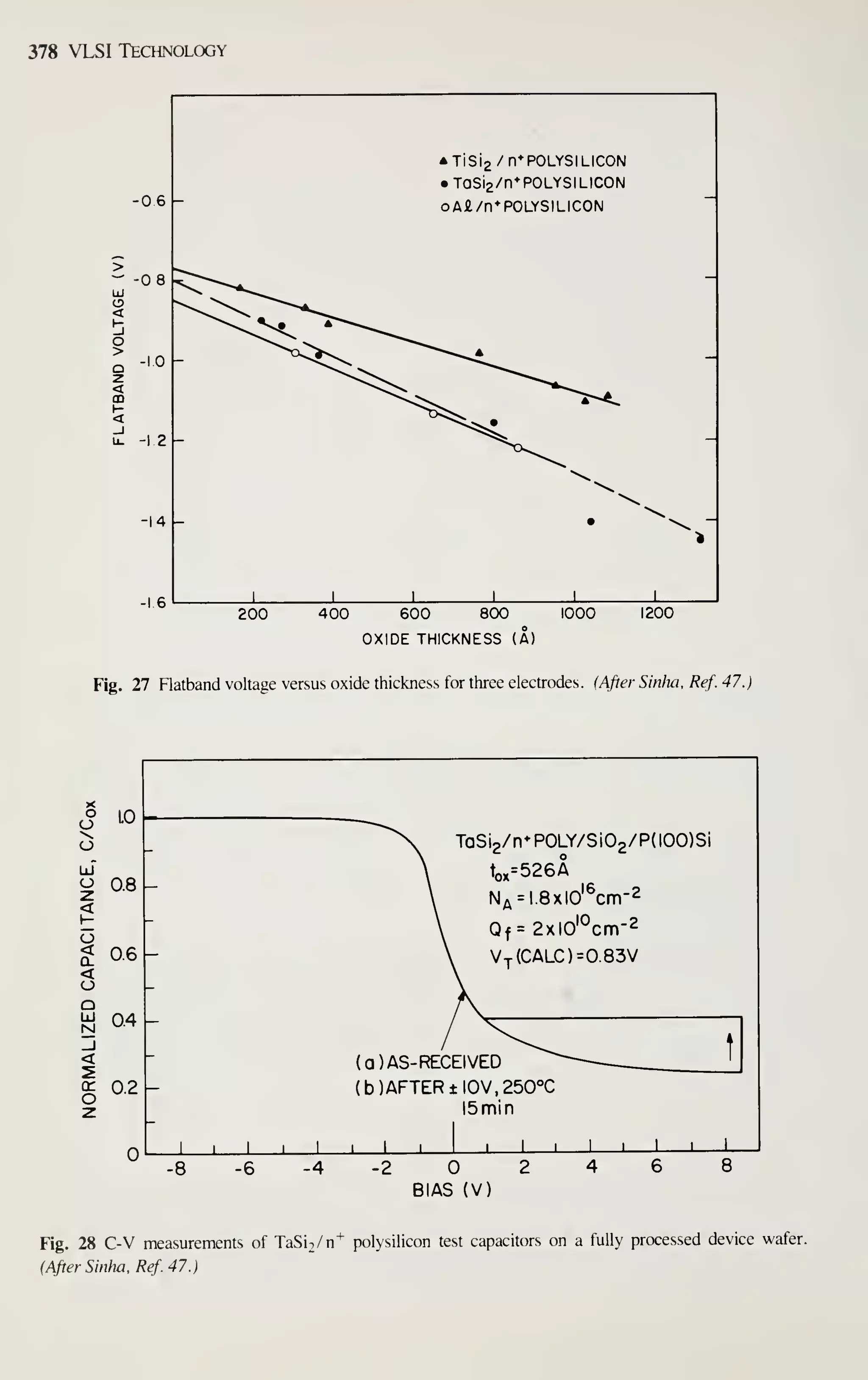
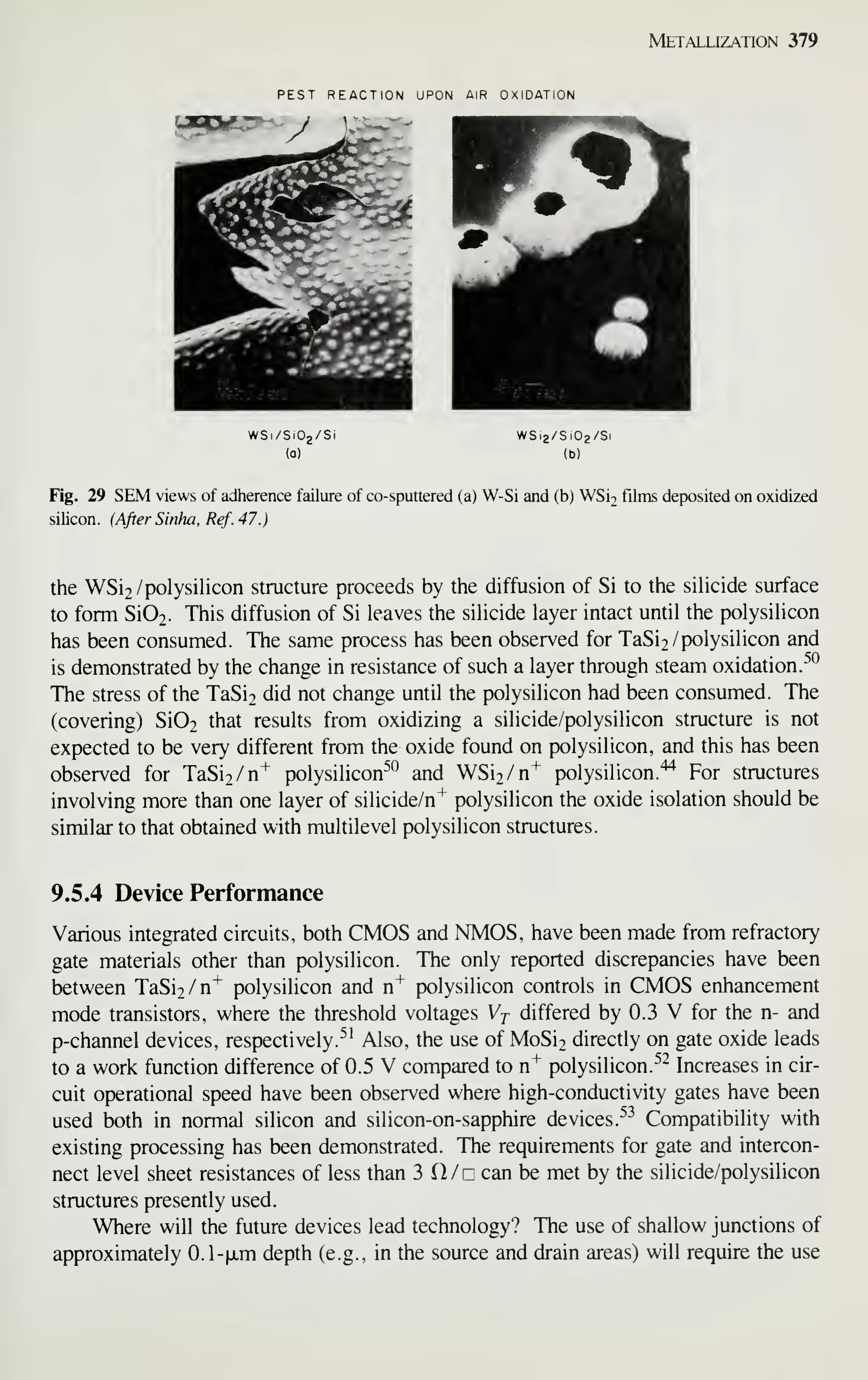
![Metallization 381
Note that the CI is not bound after the A1(0H)3 is formed, leading to further attack of
exposed Al. The problem is compounded by placing metal lines close together and
imposing an electric field between them, such as would occur in VLSI structures.
Passivation by removing residual CI is common in most Al dry-etching processes.
This residual CI may be removed by a CF4-O2 or O2 plasma treatment immediately
after etching and before exposing the wafers to the atmosphere. Further stability may
be gained by thermally oxidizing the metal. ^^ Excessive P in phosphosilicate glass
may cause formation of HPO3 on the dielectric surface, which may in turn lead to
attack of the Al alloy structure. Maintaining a maximum of 6% P content in the
dielectric minimizes this source of corrosion. Corrosive environments where the
reactants are present in the atmosphere require not only cleaning, but passivation and
encapsulation.
9.7 FUTURE TRENDS
Multi-level metallization may be necessary in order to keep VLSI chip areas to a size
compatible with reasonable yield. Cross-unders in the bulk silicon substrate may be
possible by using epitaxially grown silicon on high-conductivity silicides. These
buried high-conductivity patterns may be an alternative to additional metal layers
above the substrate surface. With the use of lower processing temperatures will come
the use of materials currently not considered (i.e., materials that are thermodynami-
cally unstable in present process sequences), such as PtSi. A major stumbling block
to an all-low-temperature process is the required high-temperature treatment to getter
impurities during the final stages of the process. Photochemical deposition may be
useful in maintaining low-temperature processing. Increased use of thermal CVD
techniques is also likely, since the more conformal nature of the films is attractive in
metal step coverage. Development of a conductor plug to remove the metal step cov-
erage problem at contact windows is another possibility. Much of the burden for
achieving practical VLSI technologies will fall on metallization, and, for the foresee-
able future, metallization will remain an active area for the introduction of new
materials and processes.
REFERENCES
[1] J. L. Vossen, Ed., Bibliography on Metallization Materials and Techniques for Silicon Devices, Thin
Film Division, American Vacuum Society, New York, 1974-1982.
[2] M. P. Lepselter, "Beam Lead Technology," Proc. Second Symposium on the Deposition of Thin
Films by Sputtering, University of Rochester, June 1967, p. 48.
[3] W. D. Ryden and E. F. Labuda, "A Metallization Providing Two Levels of Interconnect for Beam-
Leaded Silicon Integrated Circuits," IEEE J. Solid-State Circuits, SC-12, 376 (1977).
[4] S. M. Sze, Physics of Semiconductor Devices , 2d ed.. Wiley, New York, 1981, p. 304.
[5] J. F. O'Hanlon, A User's Guide to Vacuum Technology, Wiley, New York, 1980.
[6] A. S. Grove, Physics and Technology of Semiconductor Devices, Wiley, New York, 1967.
[7] R. Glang, "Vacuum Evaporation," in L. I. Maissel and R. Glang, Eds. , Handbook of Thin Film Tech-
nology, McGraw-Hill, New York, 1970, Chapter 1, p. 1-107.
[8] S. Dushman, Scientific Foundations of Vacuum Technique, Wiley New York, 1962, p. 21
.](https://image.slidesharecdn.com/simonm-220913174129-44ec6f82/75/Simon-M-Sze-editor-Very-Large-Scale-Integration-VLSI-Technology-McGraw-Hill-Inc-US-1983-pdf-401-2048.jpg)
![382 VLSI Technology
[9] R. Glang, "Vacuum Evaporation," in L. I. Maissel and R. Glang, Eds., Handbook of Thin Film Tech-
nology, McGraw-Hill, New York, 1970, Chapter 1, p. 1-26.
[10] R. Glang, "Vacuum Evaporation," in L. I. Maissel and R. Glang, Eds., Handbook of Thin Film Tech-
nology, McGraw-Hill, New York, 1970, Chapter 1, p. 1-92.
[11] J. L. Vossen and J. J. Cuomo, "Glow Discharge Sputter Deposition," in J. L. Vossen and W. Kern,
Eds., Thin Film Processes, Academic, New York, 1978, p. 12.
[12] J. A. Thornton and A. S. Penfold, "Cylindrical Magnetron Sputtering," in J. L. Vossen and W. Kern,
Eds., Thin Film Processes, Academic, New York, 1978, p. 76.
[13] D. B. Eraser, "The Sputter and S-Gun Magnetrons," in J. L. Vossen and W. Kern, Eds., Thin Film
Processes, Academic, New York, 1978, p. 115.
[14] R. K. Waits, "Planar Magnetron Sputtering," in J. L. Vossen and W. Kern, Eds., Thin Film
Processes, Academic, New York, 1978, p. 131.
[15] J. M. E. Harper, "Ion Beam Deposition," in J. L. Vossen and W. Kern, Eds., Thin Film Processes,
Academic, New York, 1978, p. 175.
[16] C. M. Melliar Smith and C. J. Mogab, "Plasma Assisted Etching Techniques for Pattern Delinea-
tion," in J. L. Vossen and W. Kem, Eds., Thin Film Processes, Academic, New York, 1978, p. 497.
[17] J. L. Vossen and J. J. Cuomo, "Glow Discharge Sputter Deposition," in J. L. Vossen and W. Kem,
Eds., Thin Film Processes, Academic, New York, 1978, p. 50.
[18] T. N. Kennedy, "Sputtered Insulator Film Contouring over Substrate Topography" , J. Vac. Sci. Tech-
nol.,13, 1135(1976).
[19] W. Kem and V. S. Ban, "Chemical Vapor Deposition of Inorganic Thin Fikns," in J. L. Vossen and
W. Kem, Eds., Thin Film Processes, Academic, New York, 1978, p. 258.
[20] A. C. Adams, Chapter 3, this volume.
[21] J. M. Shaw and J. A. Amick "Vapor Deposited Tungsten For Devices," RCA Review, 31, 306
(1970).
[22] C. F. Powell, "Chemically Deposited Metals," in C. F. Powell, J. H. Oxley, and J. M. Blocher,
Eds., Vapor Deposition, Wiley, New York, 1966, p. 277.
[23] N. E. Miller and I. Beinglass, "Hot-Wall CVD Tungsten for VLSI," Solid State TechnoL, 23, 79
(1980).
[24] I. A. Blech, D. B. Eraser, and S. E. Haszko, "Optimization of Al Step Coverage Through Computer
Simulation and Scanning Electron Microscopy," J. Vac. Sci. TechnoL, 15, 13 (1978); Errata, J. Vac.
Sci. TechnoL, 15, 1856(1978).
[25] W. Fichtner, Chapter 10, this volume.
[26] A. C. Adams, "Plasma Planarization," Solid State TechnoL, 24, 178 (1981).
[27] T. Sakurai and T. Serikawa, "Lift-Off Metallization of Sputtered Al Alloy Fihns," J. Electrochem.
Soc.,126, 1257(1979).
[28] T. Batchelder, "A Simple Metal Lift-Off Process," Solid State TechnoL, 25, 1 1 1 (1982).
[29] Handbook of Chemistry and Physics, Chemical Rubber Co., Cleveland, 1970.
[30] K. N. Tu, "Shallow And Parallel Silicide Contacts," J. Vac. Sci. TechnoL, 19, 766 (1981).
[31] A. K. Sinha, W. S. Lindenberger, D. B. Eraser, S. P. Murarka, and E. N. Fuls, "MOS Capability of
High Conductivity TaSij/n^ Poly Si Gate MOSFET", IEEE Trans. Electron Devices, ED-27, 1425
(1980).
[32] M.-A. Nicolet and M. Bartur, "Diffusion Barriers in Layered Contact Stmctures," J. Vac. Sci. Tech-
noL, 19, 186(1981)
[33] M. Wittmer, "High-Temperature Contact Stmctures for Silicon Semiconductor Devices," v^p/. Phys.
Lett., 37, 540(1980).
[34] P. B. Ghate, J. C. Blair, C. R. Fuller, andG. E. McGuire, "AppHcationofTiiW Barrier Metallization
For Integrated Circuits," Thin Solid Films, 53, 117(1978).
[35] J. Black, "Physics of Electromigration," Proc. 12th Reliability Physics Symposium, IEEE, New
York, 1974, p. 142.
[36] S. Vaidya, D. B. Eraser, and A. K. Sinha, "Electromigration Resistance of Fine Line Al," Proc. 18th
Reliability Physics Symposium, IEEE, New York, 1980, p. 165.
[37] A. Gangulee, P. S. Ho, and K. N. Tu, Eds., Low Temperature Diffusion and Application to Thin
Films, Elsevier, New York, 1975.](https://image.slidesharecdn.com/simonm-220913174129-44ec6f82/75/Simon-M-Sze-editor-Very-Large-Scale-Integration-VLSI-Technology-McGraw-Hill-Inc-US-1983-pdf-402-2048.jpg)
![Metallization 383
[38] S. Vaidya, "Electromigration in Aluminum/Poly-silicon Composites," Appl. Phys. Lett., 39, 900
(1981).
[39] P. B. Ghate, J. C. Blair, and C. R. Fuller, "Metallization In Microelectronics," Thin Solid Films, 45,
69(1977).
[40] R. C. Henderson, R. F. W. Pease, A. M. Voschenkov, R. P. Helm, and R. Wadsack, "A High Speed
P-channel Random Access 1024 Bit Memory Made with Electron Lithography," IEEE Solid-State Cir-
cuits, SC-10, 92 (1915).
[41] D. M. Brown, W. E. Engler, M. Garfinkel, and P. V. Gray, "Self-Registered Molybdenum-Gate
MOSFET," J. Electrochem. Soc, 115, 874 (1966).
[42] S. P. Murarka and D. B. Eraser, "Silicide Formation in Thin Cosputtered (Titanium + Silicon) Fihns
on Polycrystalline Silicon and Si04," J. Appl. Phys., 51, 350 (1980).
[43] K. L. Wong, T. C. HoUoway, R. F. Pinizotto, Z. P. Sobczak, W. R. Hunter, and A. F. Tasch, "Com-
posite TiSi2/« ^ Poly-Si Low Resistivity Gate Electrode and Interconnect for VLSI Device Technol-
ogy," IEEE Trans. Electron Devices. ED-29, 547 ( 1982).
[44] B. L. Crowder and S. Zirinsky, "l-jjim MOSFET VLSI Technology: Part VH-Metal Silicide Inter-
connection Technology—A Future Perspective," IEEE J. Solid State Circuits, SC-14, 291 (1979).
[45] T. Mochizuki, K. Shibata, T. Inoue, and K. Ohuchi, "A New MOS Process Using MoSi2 As A Gate
Material," yp«. J. Appl. Phys., 77 (suppl. 17-1) 37 (1977).
[46] S. P. Murarka, D. B. Eraser, A. K. Sinha, and H. J. Levinstein, "Refractory Silicides of Titanium and
Tantalum for Low Resistivity Gates and Interconnects," IEEE Trans. Electron Devices, ED-27, 1409
(1980).
[47] A. K. Sinha, "Refractory Metal Silicides for VLSI Applications," J. Vac. Sci. Technol., 19, 778
(1981).
[48] S. P. Murarka, "Refractory Silicides for Integrated Circuits," J. Vac. Sci. Technol., 17, 775 (1980).
[49] T. F. Retajczyk and A. K. Sinha, '
Elastic Stiffness and Thermal Expansion Coefficients of Various
Refractory Silicides and Silicon Nitride Films," Thin Solid Films, 70, 241 (1980).
[50] S. P. Murarka, D. B. Eraser, W. S. Lindenberger, and A. K. Sinha, "Oxidation of Tantalum Disili-
cide on Polycrystalline Silicon," 7. Appl. Phys., 51, 3241 (1980).
[51] D. B. Eraser, S. P. Murarka, A. R. Tretola, and A. K. Sinha, "Tantalum Silicide/Polycrystalline
Silicon-High Conductivity Gates for CMOS LSI Applications," J. Vac. Sci. Technol., 18, 345 ( 1981).
[52] T. Mochizuki, T. Tsujimaru. M. Kashiwagi, and Y. Nishi, "Film Properties of MoSi2 and Their
Application to Self-Aligned MoSi2 Gate MOSFET," IEEE Trans. Electron Devices, ED-27, 1431
(1980).
[53] B. C. Leung and J. S. Maa, "Refractory Metal Sihcide/N+ Polysilicon in CMOS/SOS," Tech. Digest
Int. Elect., Sn{l9Sl).
[54] C. J. Koeneke, S. M. Sze, R. M. Levin, and E. Kinsbron, "Schottky MOSFET for VLSI," paper
15.6, IEEE Electron Device Meeting, Washington, D. C, Dec. 1981.
[55] R. Kieffer and F. Benesovsky, Hartstojfe, Springer, Vienna, 1963.
[56] D.-Y. Shih and P. J. Ficabora, "The Reduction of Au-Al IntermetaUic Formation and Electromigra-
tion in Hydrogen Environments," IEEE Trans. Electron Devices, ED-26, 27 (1979).
[57] J. M. Eldridge, "Corrosion Problems of Metal Conductor Lines in Integrated Circuits," Solid State
Devices, Inst. Phys. Conf. Ser. No. 57, 1980, p. 211.
[58] M. Hansen, Constitution ofBinary Alloys, McGraw-Hill, New York, 1958.
PROBLEMS
1 If the residual water vapor pressure is 5 x 10~^ Pa in an Al evaporation station at 300 K, what O content
does a deposited film have if Al is deposited at 50 A /s? Assume the reaction results in incorporating AI2 O3
in the film and that each Ht O molecule has a reaction probability 10"''.
2 Assume thai you have no way of co-depositing Al-Si while maintaining the compositional ratio
throughout the film thickness. However, individual discrete films may be deposited with accurate thickness.
A sandwich of 1 [jtm of Al on a Si film must be deposited on a Si contact. It must be stable so that sintering](https://image.slidesharecdn.com/simonm-220913174129-44ec6f82/75/Simon-M-Sze-editor-Very-Large-Scale-Integration-VLSI-Technology-McGraw-Hill-Inc-US-1983-pdf-403-2048.jpg)
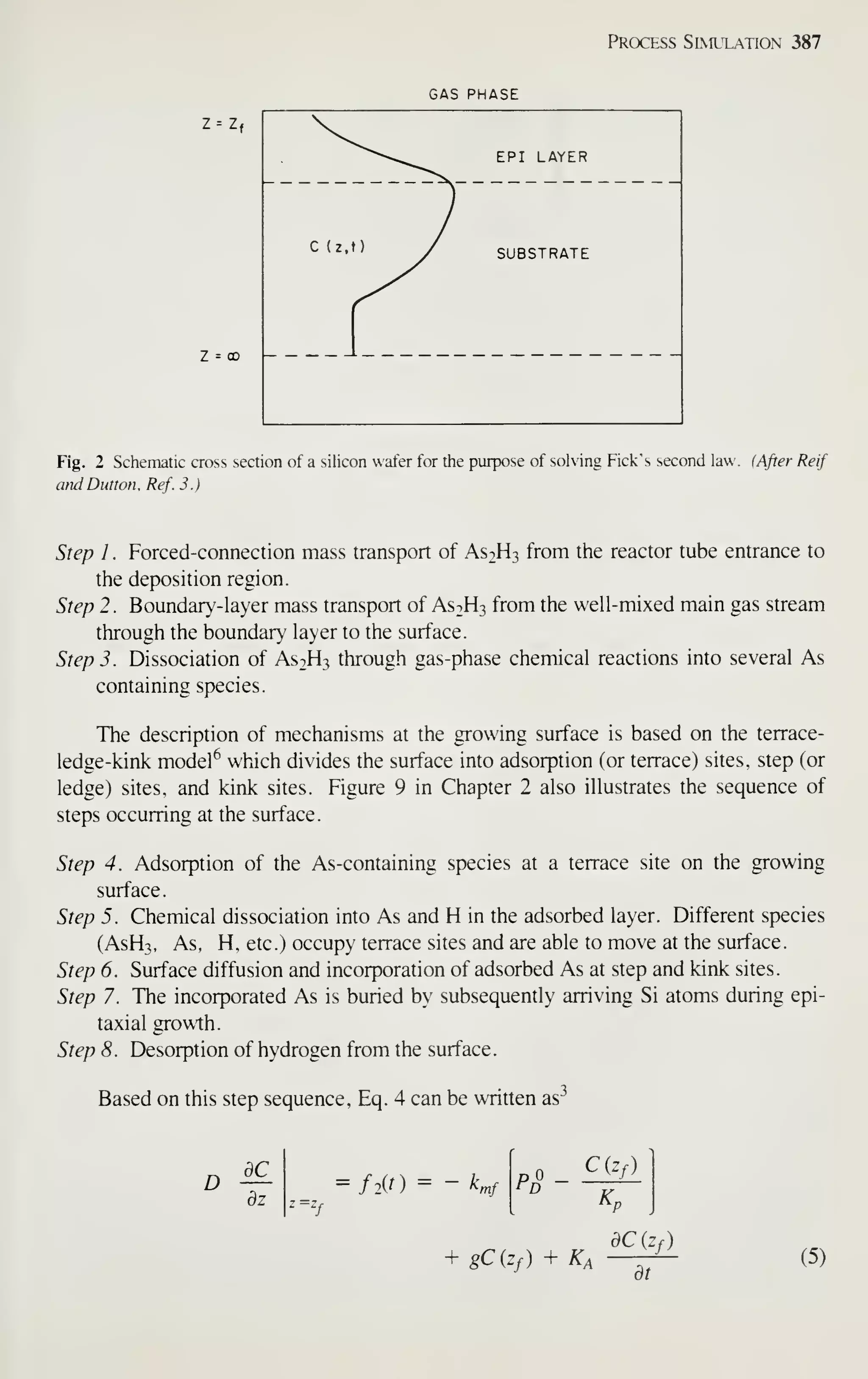
![388 VLSI Technology
The first term describes the flux of dopant species leaving the boundary layer by
adsorbing at the surface (steps 4 through 6). The variable k,nf is a kinetic coefficient
associated with the mechanism dominating the dopant-incorporation process. P^ is
the input partial pressure, C (zy) is the dopant concentration at the interface, and Kp is
a segregation coefficient relating the epitaxial dopant concentration to the concentra-
tion of dopant species in the gas phase. The second term gC (Zf) represents the rate at
which the adsorbed layer decreases its concentration of dopant species due to the sili-
con covering step (step 7). The last term represents diffusion of dopant atoms
between the adsorbed layer and the bulk silicon. The variable K^ relates the epitaxial
dopant concentration to the concentration of the dopant species in the adsorbed layer.
Pick's second law (Eq. 1) can now be solved subject to the boundary and initial
conditions, specified in Eqs. 2 to 5.
10.2.2 Computer Implementation and Results
Figure 3 shows schematically a finite difference discretization of the simulation
region. The silicon region is partitioned into discrete spatial cells with a constant
dopant concentration within each cell [that is, C = Q + i
for (z, + Z/ + i)/2
^z ^ (z,+i + z,+2)/2].
At the initial time t = 0, the doping profile is given by Eq. 2. The simulation
starts by adding a new cell z, _i (Fig. 3b). The dopant concentration C, _i of this new
cell is computed from Eq. 5 by setting the left-hand side to zero
= k^f P -gC,_i-^^-^^ (6)
This equation accounts only for dopant introduction into the added cell and neglects
the simultaneous impurity redistribution in the silicon. Now we calculate the impur-
ity redistribution that occurs during the growth of all z, _| cells by solving Fick's law
(Eq. 1). This is illustrated in Fig. 3c. No flux of impurities enters the silicon at this
time. This concludes the calculation at one time step Ar, and we arrive at
t = f + ^ ^ where we start the cycle over until the total epitaxial deposition time is
over.
Figure 4 compares a doping profile simulated by using this model with a profile
measured by the spreading resistance technique. For the comparison shown in the fig-
ure, two consecutive independent arsenic-doped epitaxial films were deposited as
indicated in the inset. The arsine flows corresponding to the first and second layers
were adjusted to produce epitaxial doping levels of approximately lO''' and
10^^ cm"-', respectively.
Between the end of the first deposition cycle and the beginning of the second, the
reactor was purged with H2 for 8 min at 1050°C. The transition between the high and
low doping levels is typical if a lightly doped layer is grown epitaxially on top of a
heavily doped substrate or buried layer. This transition is at first abrupt and then
becomes gradual. This graded transition is a result of the autodoping phenomenon.](https://image.slidesharecdn.com/simonm-220913174129-44ec6f82/75/Simon-M-Sze-editor-Very-Large-Scale-Integration-VLSI-Technology-McGraw-Hill-Inc-US-1983-pdf-408-2048.jpg)
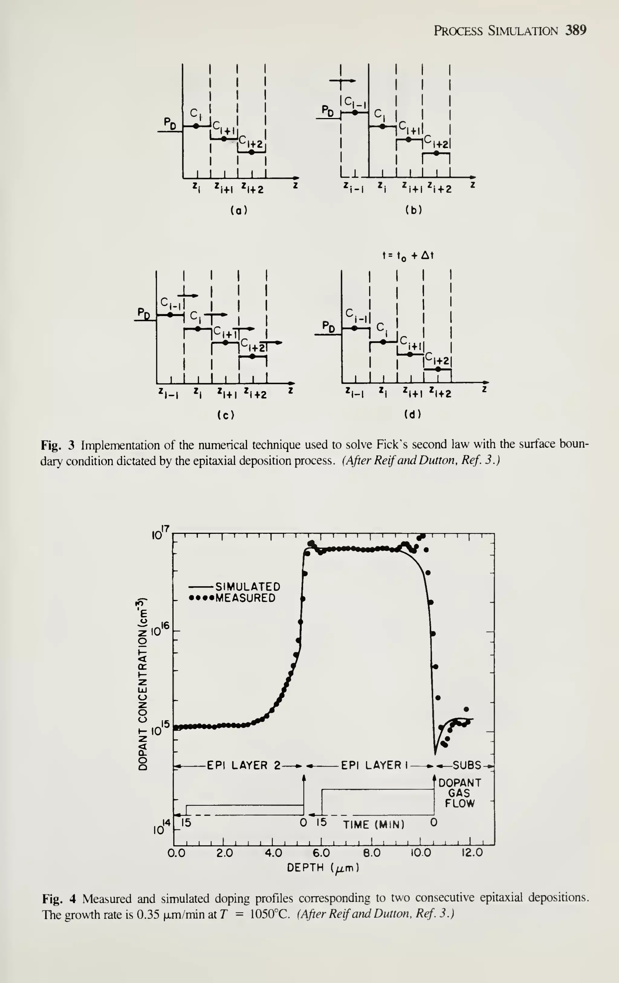
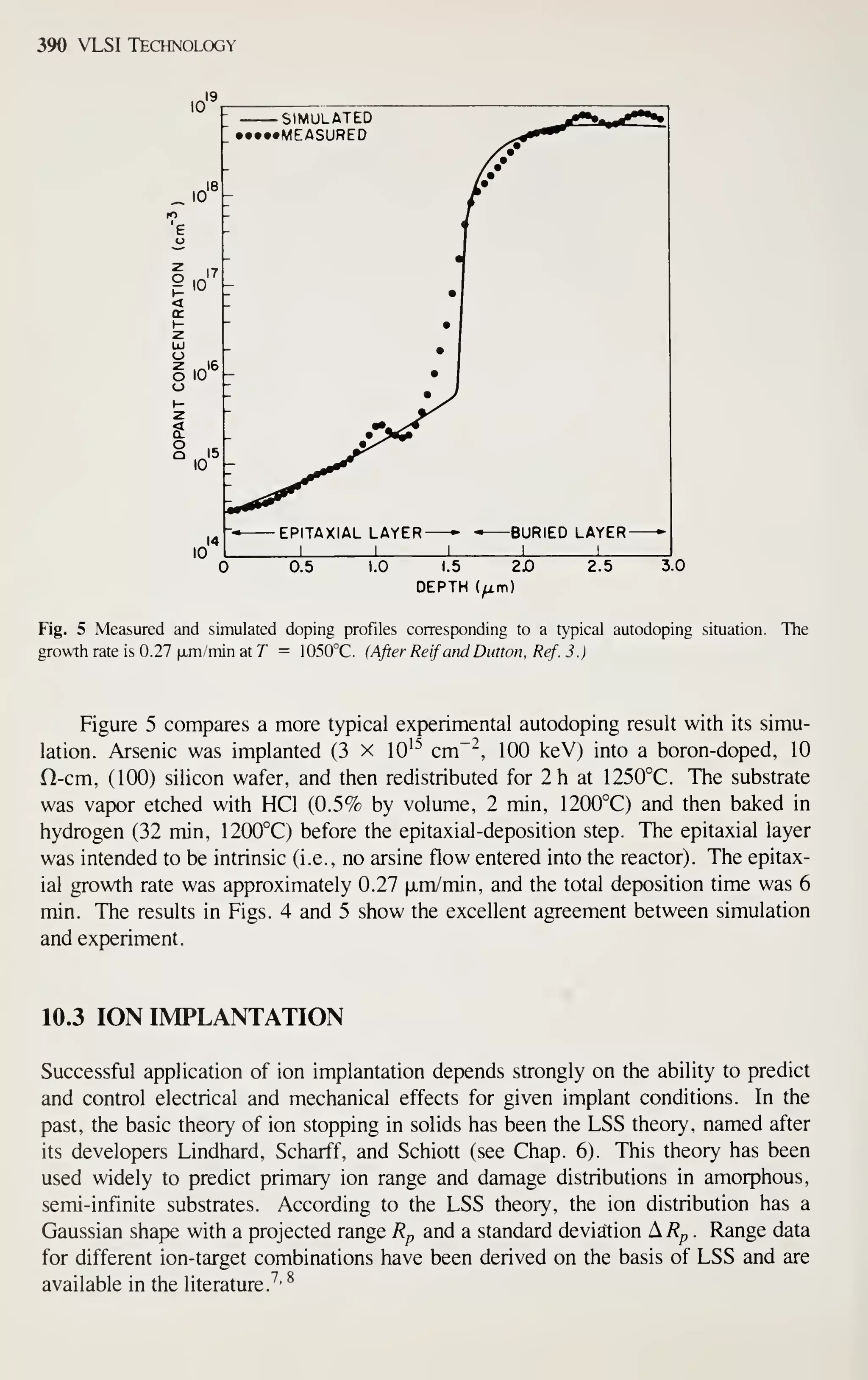
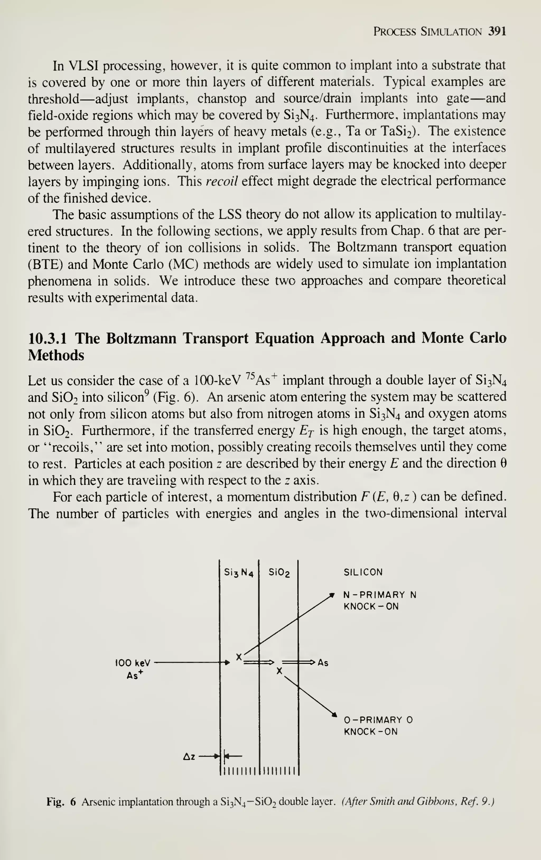
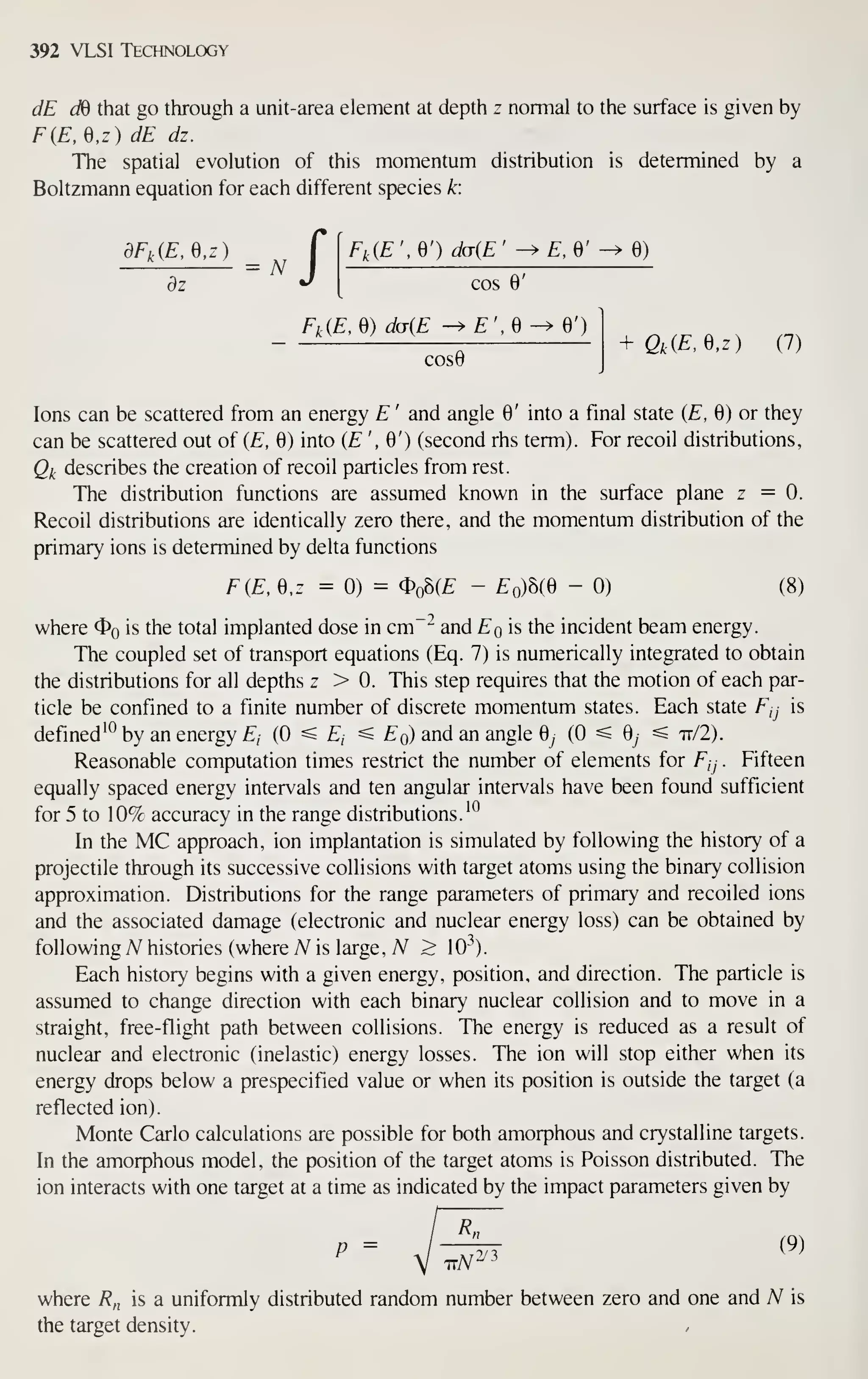
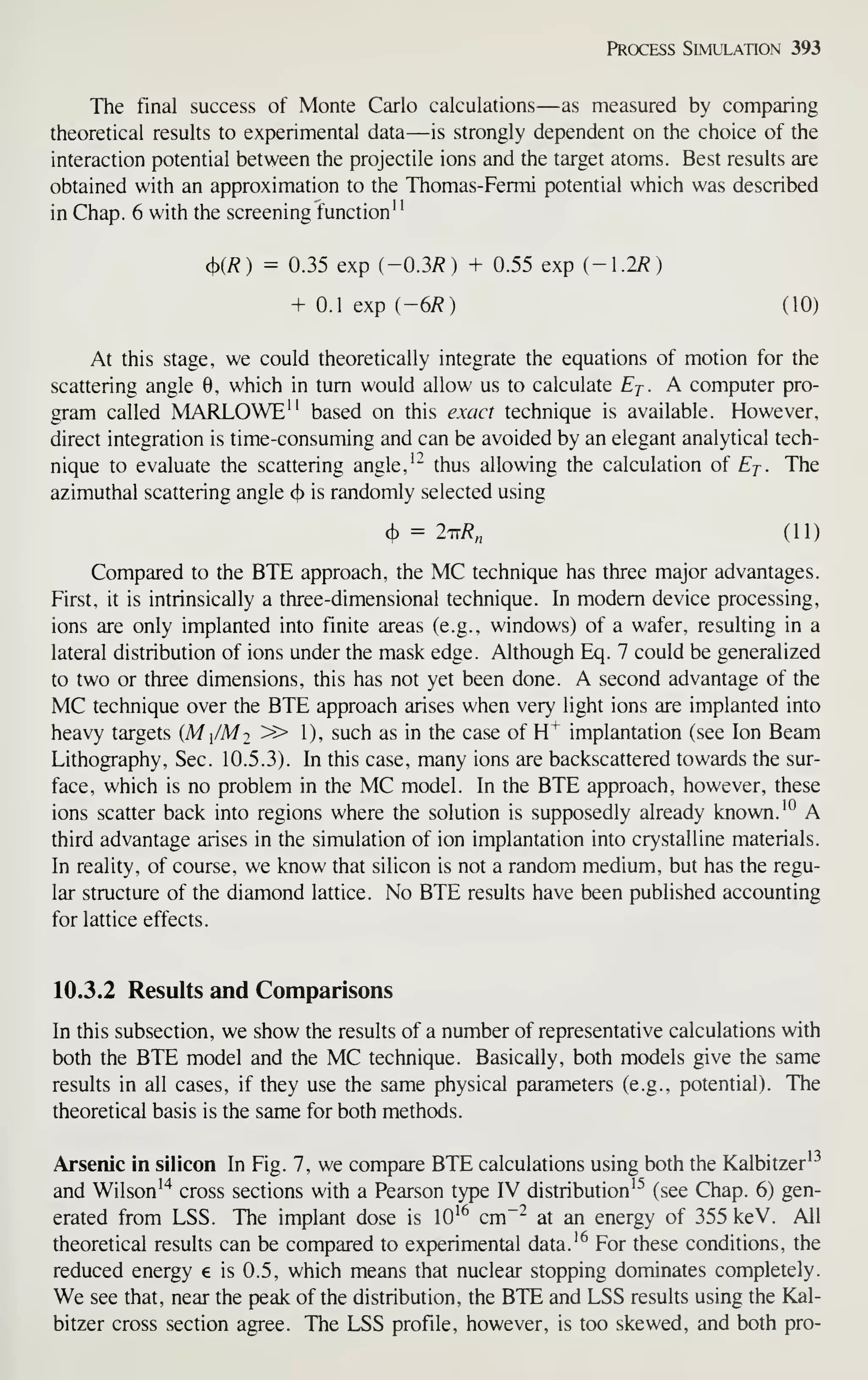
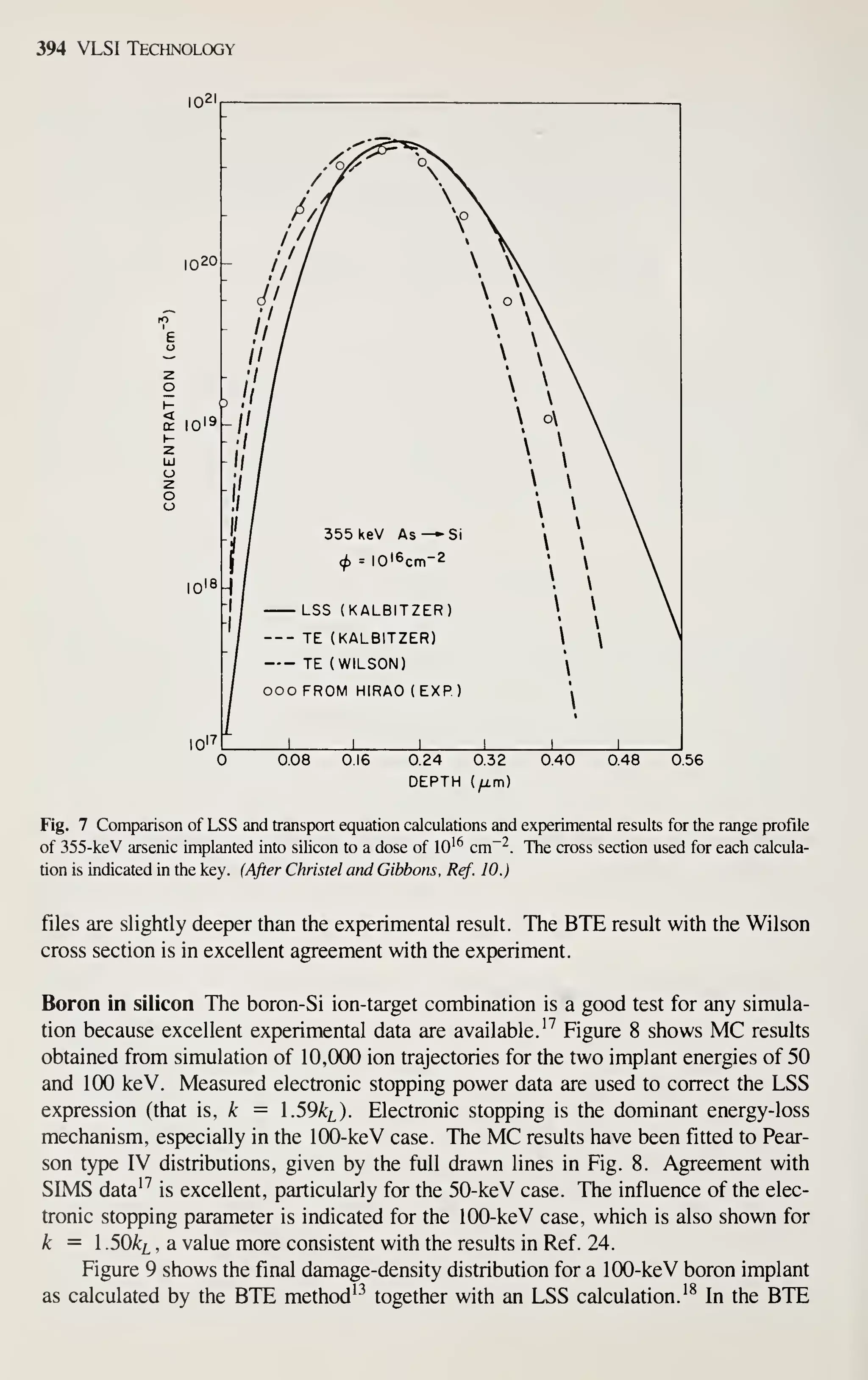
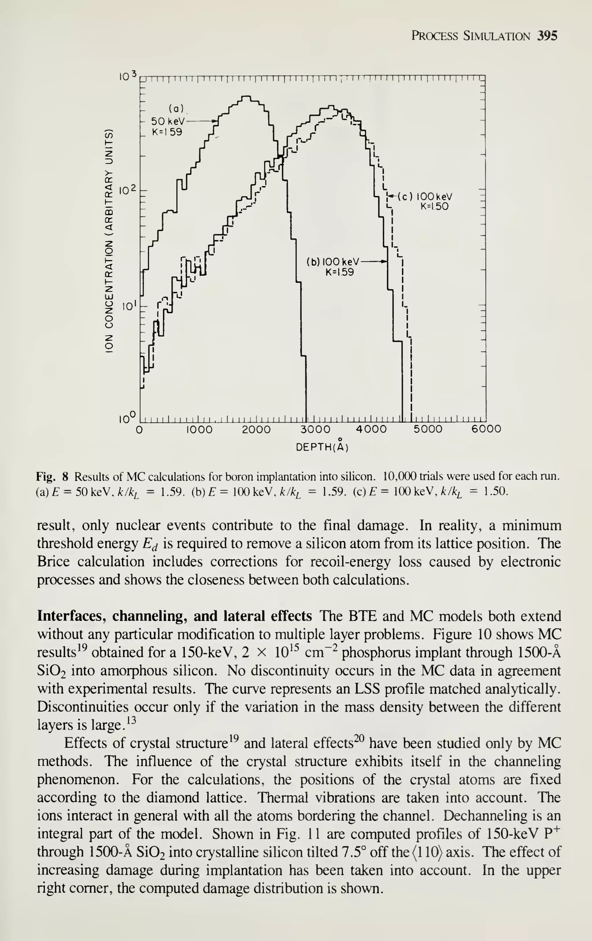
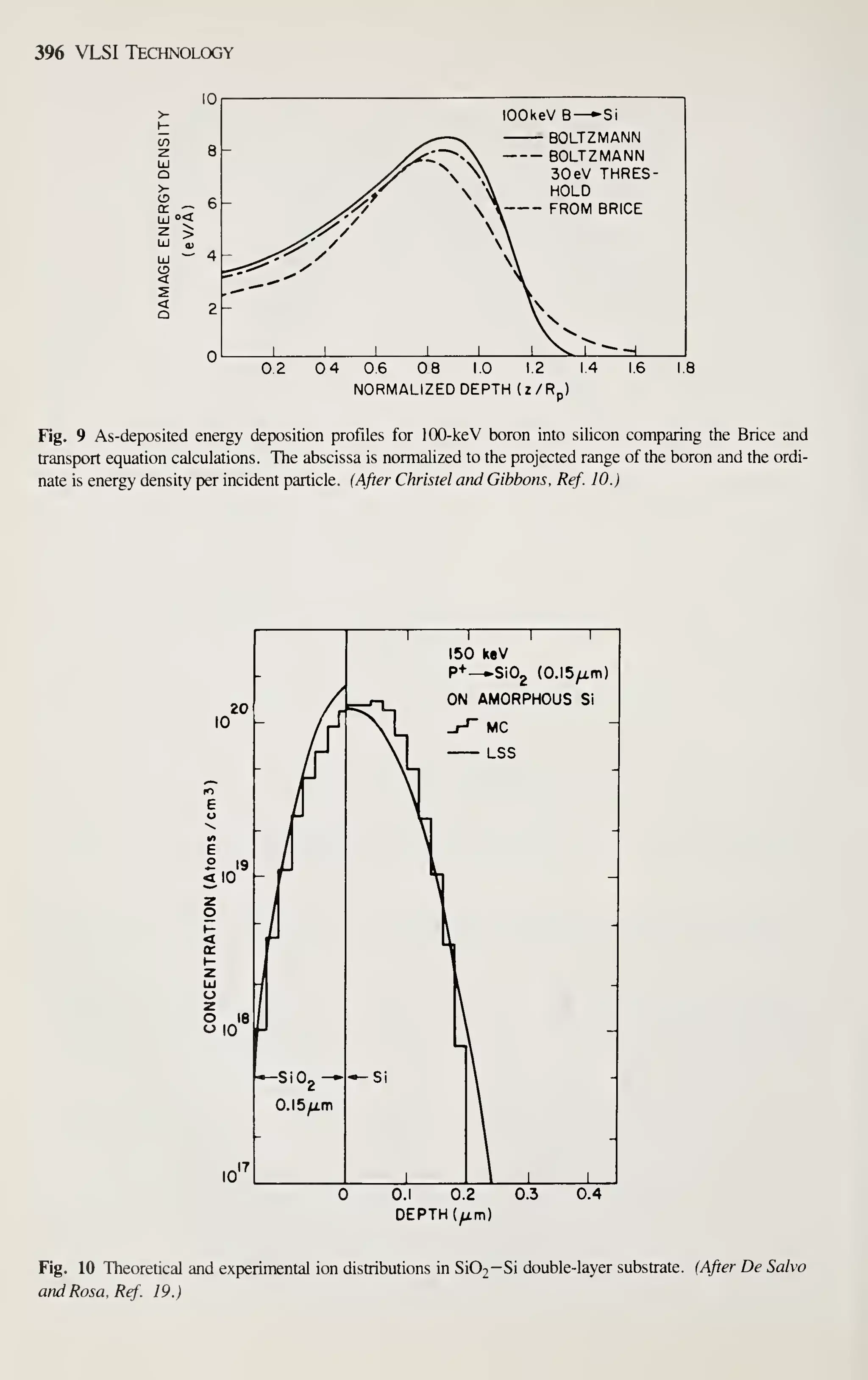
![Process Simulation 397
"1 1
] r
NO DAMAGE
WITH DAMAGE
ICX)
!: 80
UJ
o
<
1 60
<
o
^ 40h
^ 20|-
0.1 0.2
DEPTH (^m)
n
!
"^, J
01 2 0.3 0.4
DEPTH (^m)
05 06
Fig. 11 Computed penetration profile of 150-keV P^ in Si02 (0. 15 p.m) on Si crystal tilted at 7.5° off the
(110) axis, taking into account the effect of increasing damage during implantation for a total dose of
2 X 10'^ ions cm"- (continuous histogram). The inset shows the damage distribution vs. depth. (After De
Salvo arid Rosa. Ref. 19.)
10.4 DIFFUSION AND OXIDATION
Solid-state diffusion is the physical mechanism that is responsible for the impurity
migration within the silicon crystal during high-temperature processing. Together
with ion implantation and epitaxy, solid-state diffusion is one of the key methods for
controlling the type, concentration level, and distribution of impurities within specific
regions of the silicon wafer. To obtain a diffused layer, impurity atoms are intro-
duced into the surface region either by a predeposition step or by ion implantation.
For VLSI devices, ion implantation is the preferred method since it allows both accu-
rate control of the amount of dopant introduced and considerable freedom in the
profile position (by a suitable choice of implant energy). A high-temperature step is
usually required to activate the implanted ions and to remove the damage associated
with the implant process (see Chap. 6).
As we have seen above, implantations are often performed through mask win-
dows which make the diffusion process a two-dimensional problem.-^'](https://image.slidesharecdn.com/simonm-220913174129-44ec6f82/75/Simon-M-Sze-editor-Very-Large-Scale-Integration-VLSI-Technology-McGraw-Hill-Inc-US-1983-pdf-417-2048.jpg)
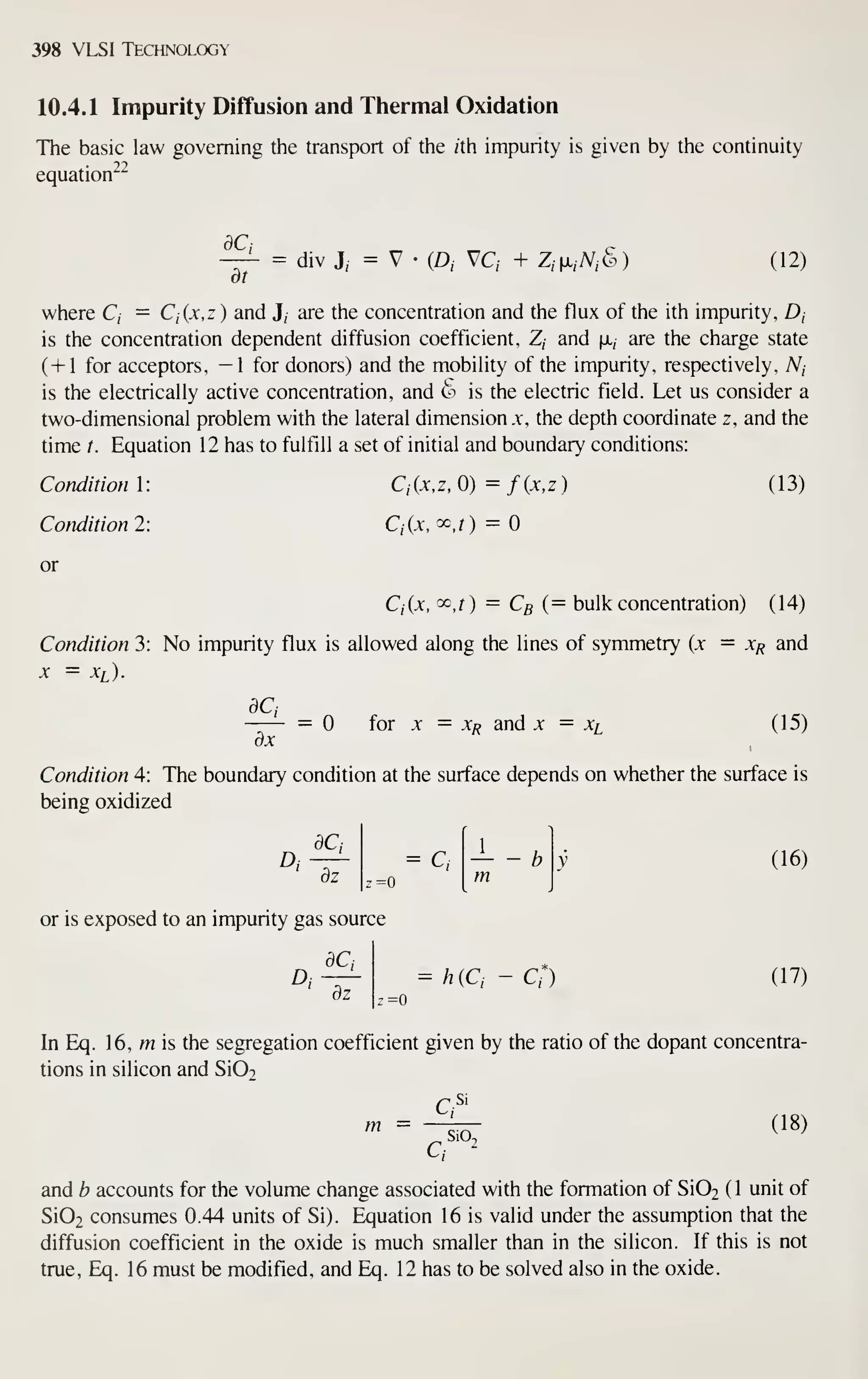
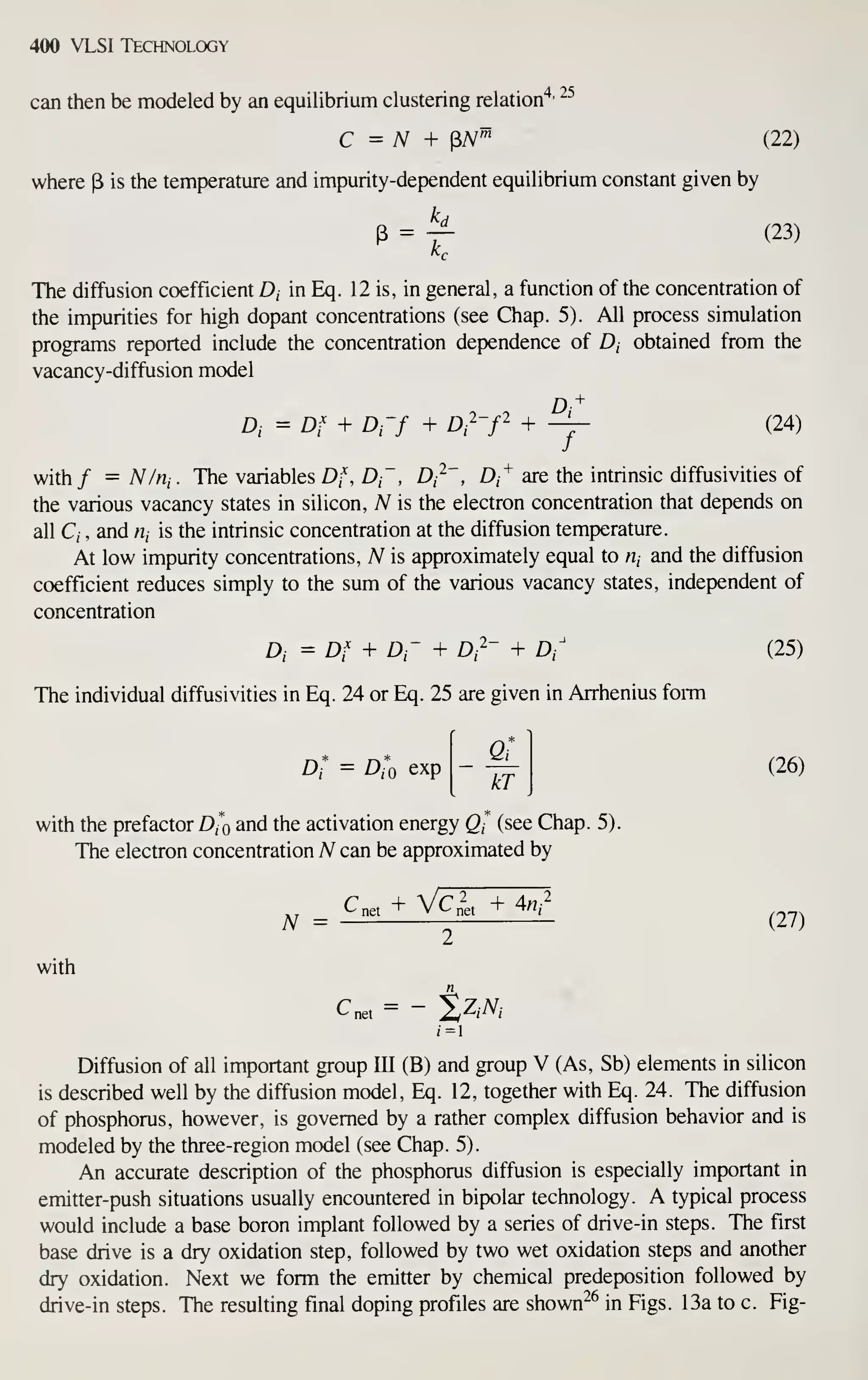
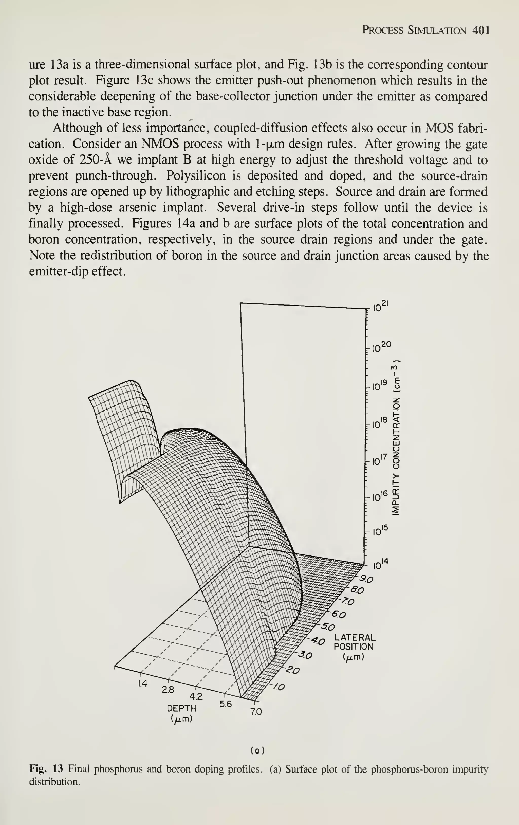
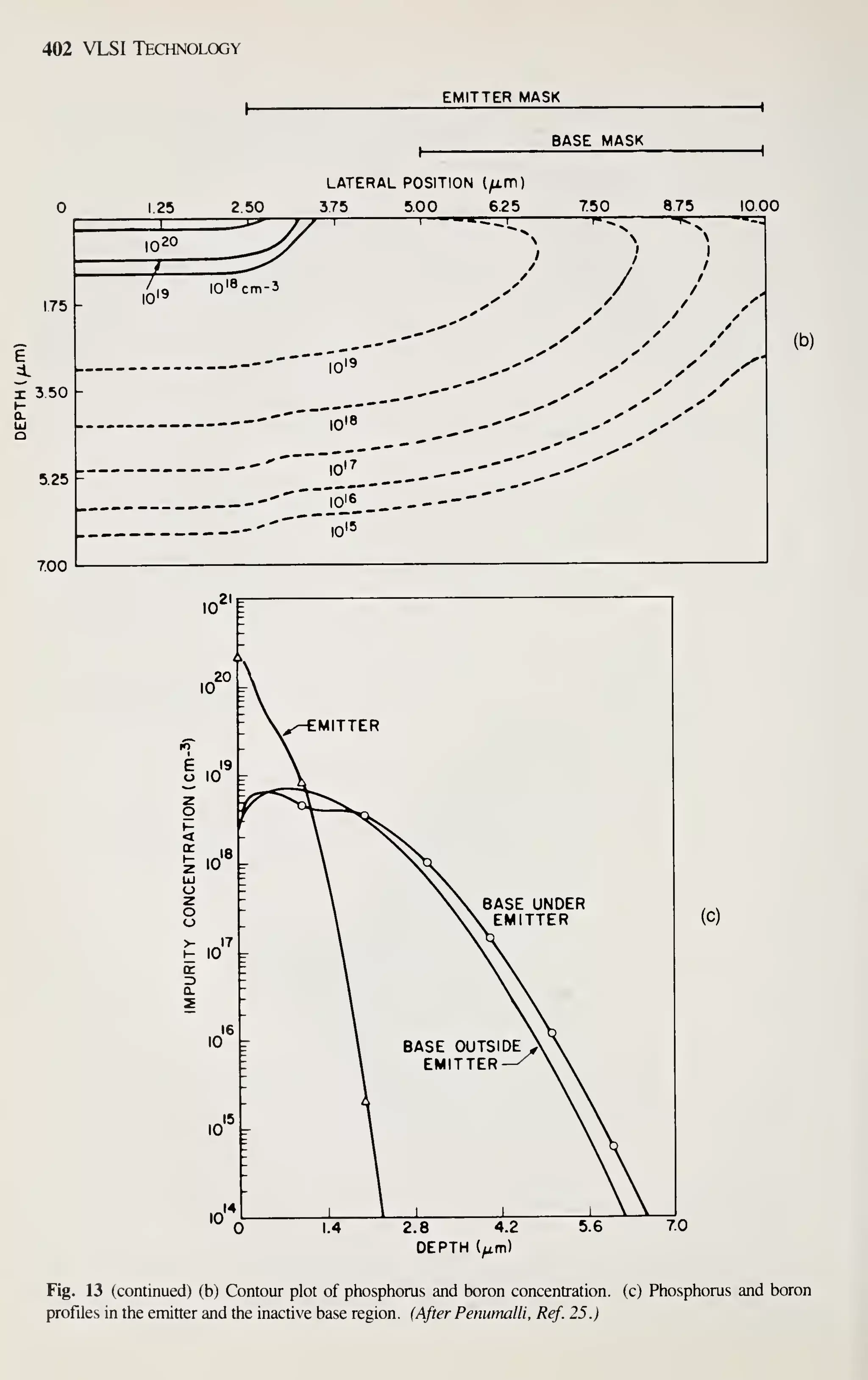
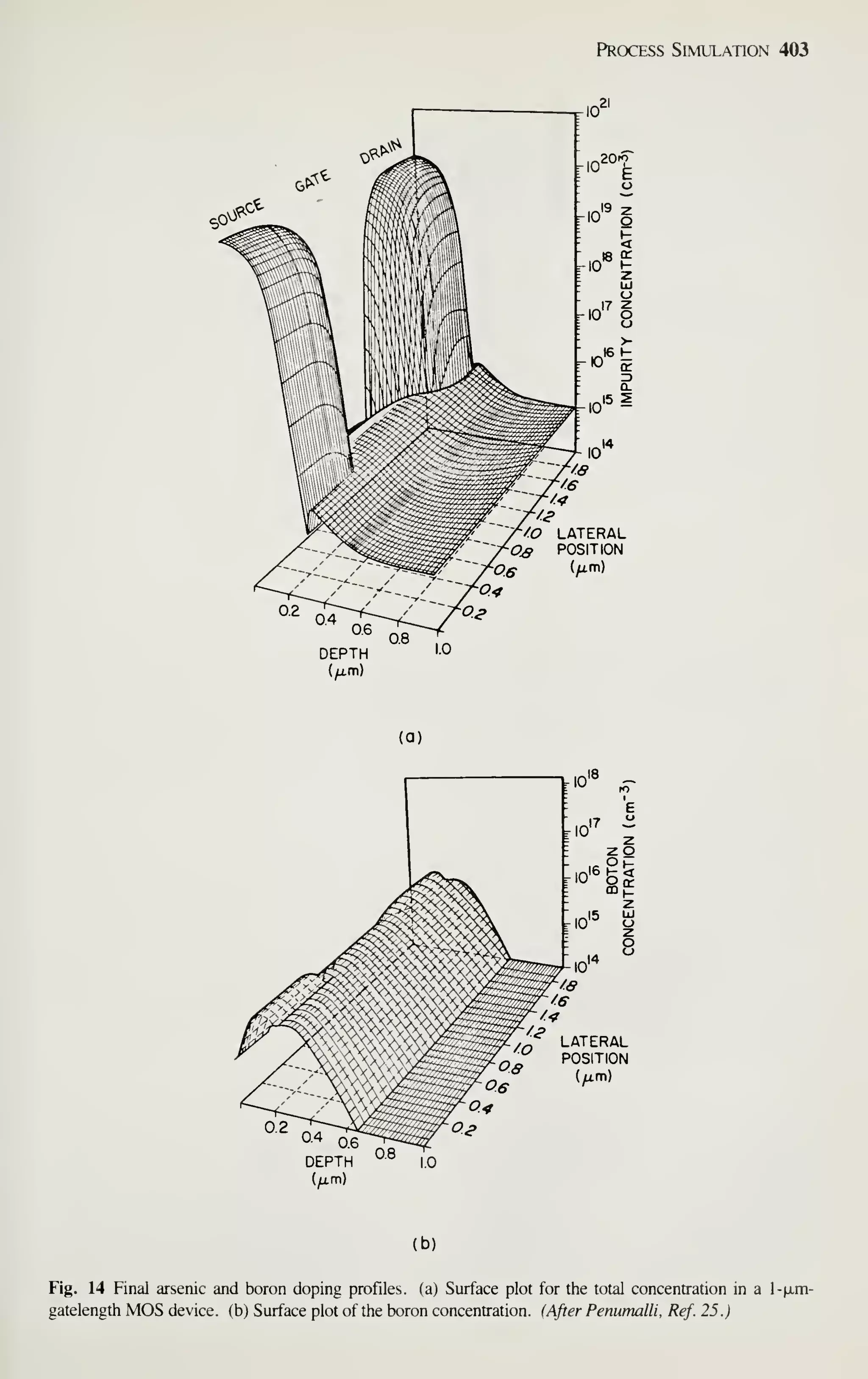
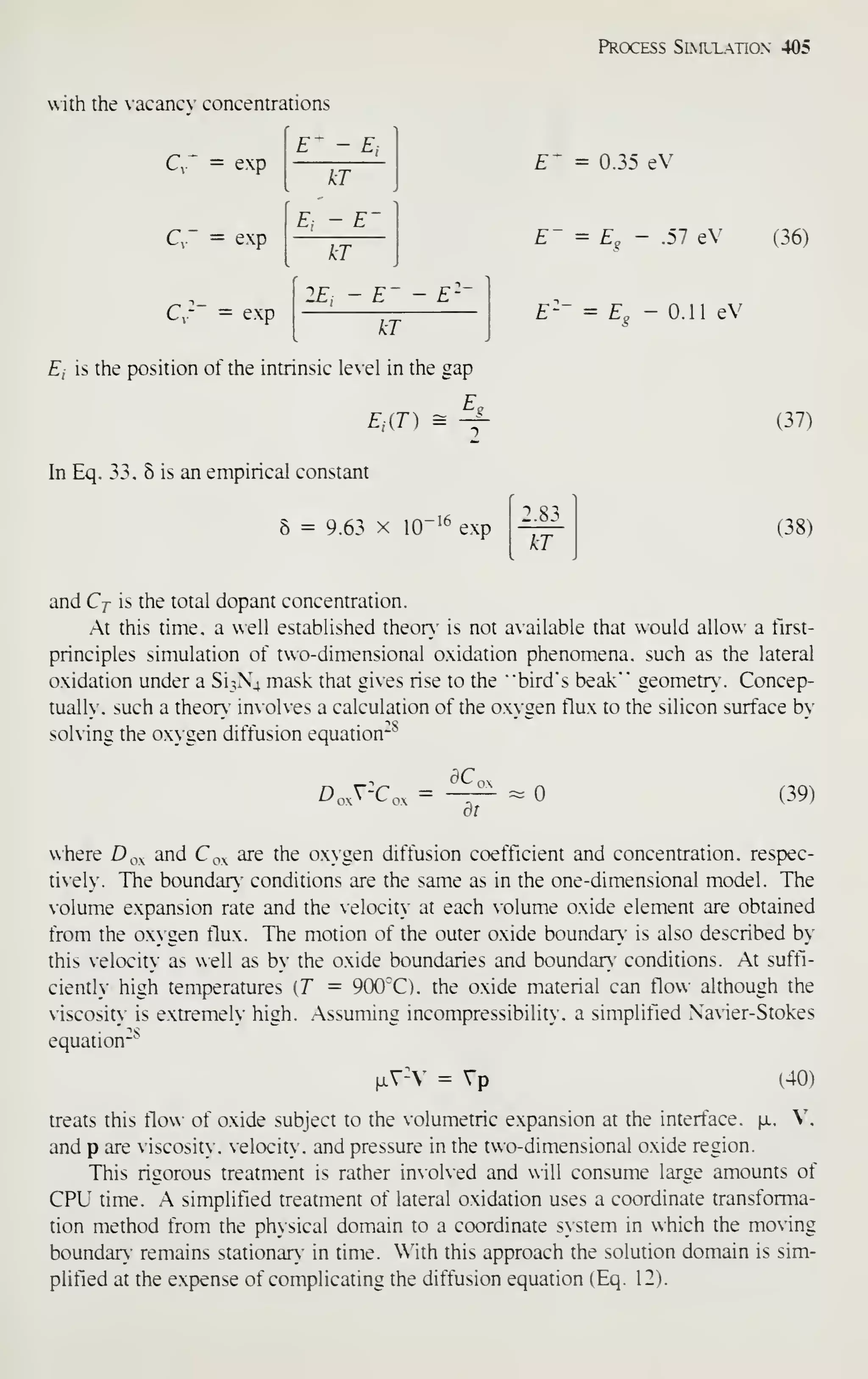
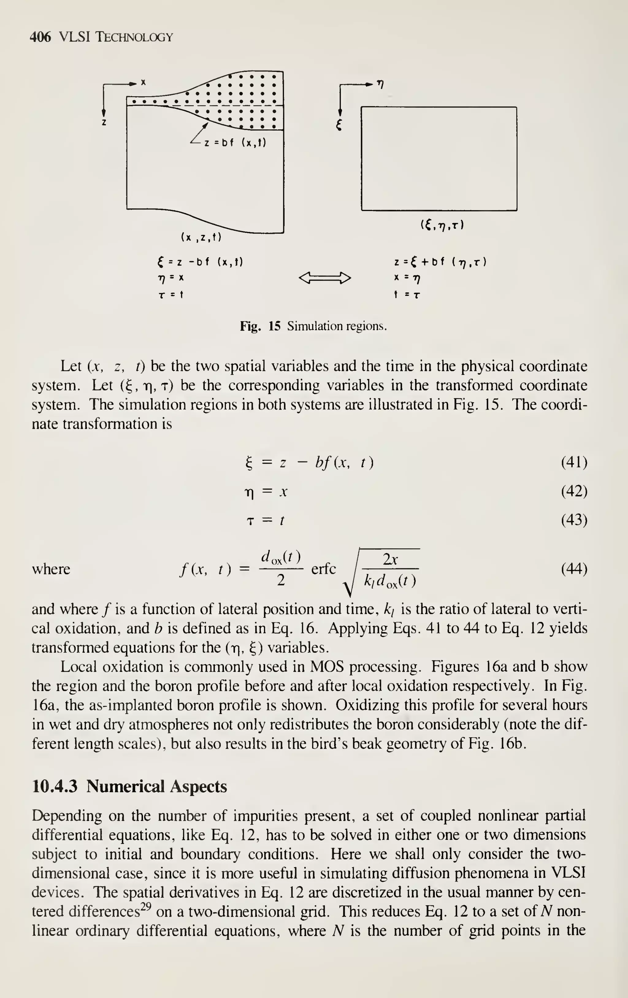
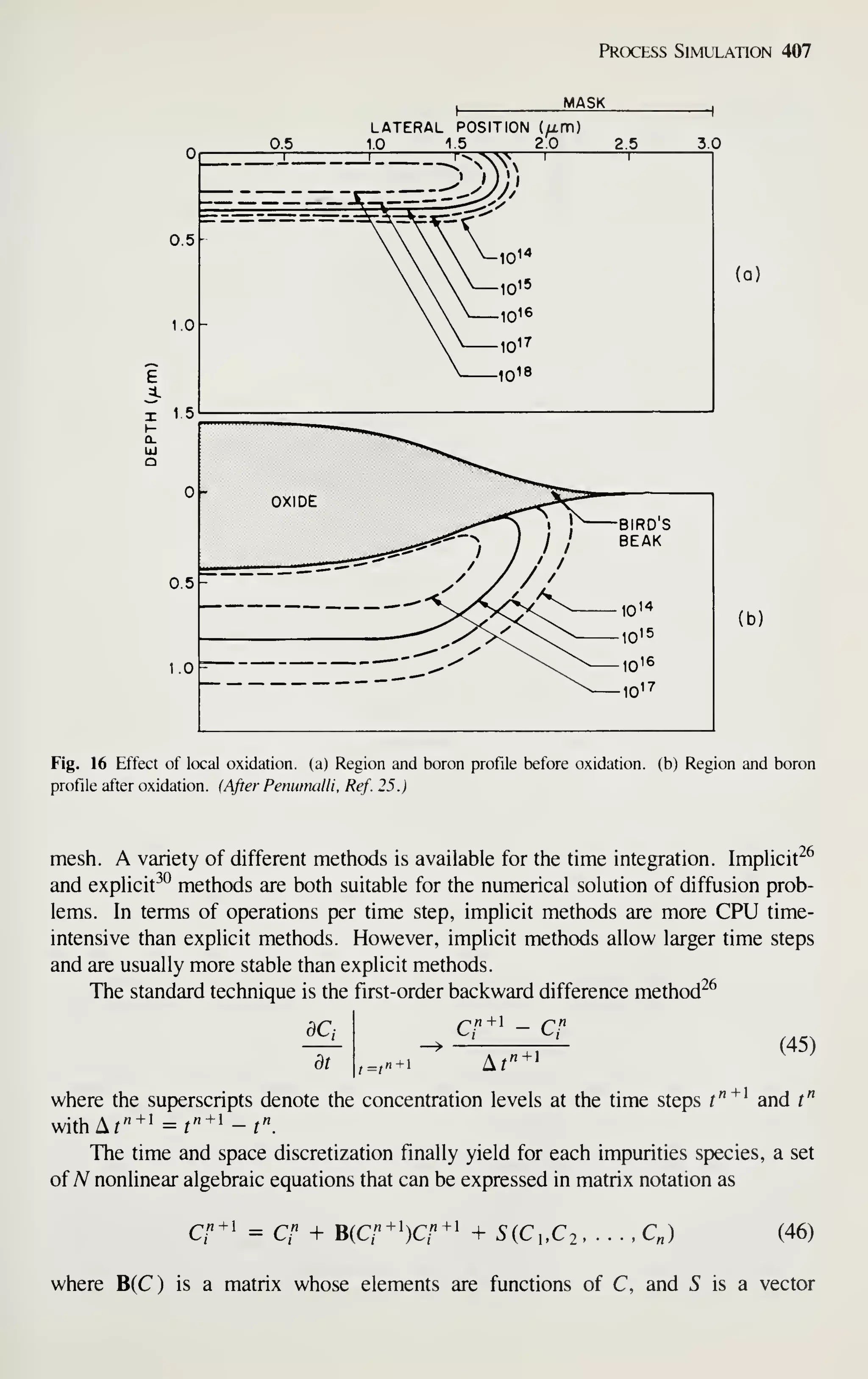
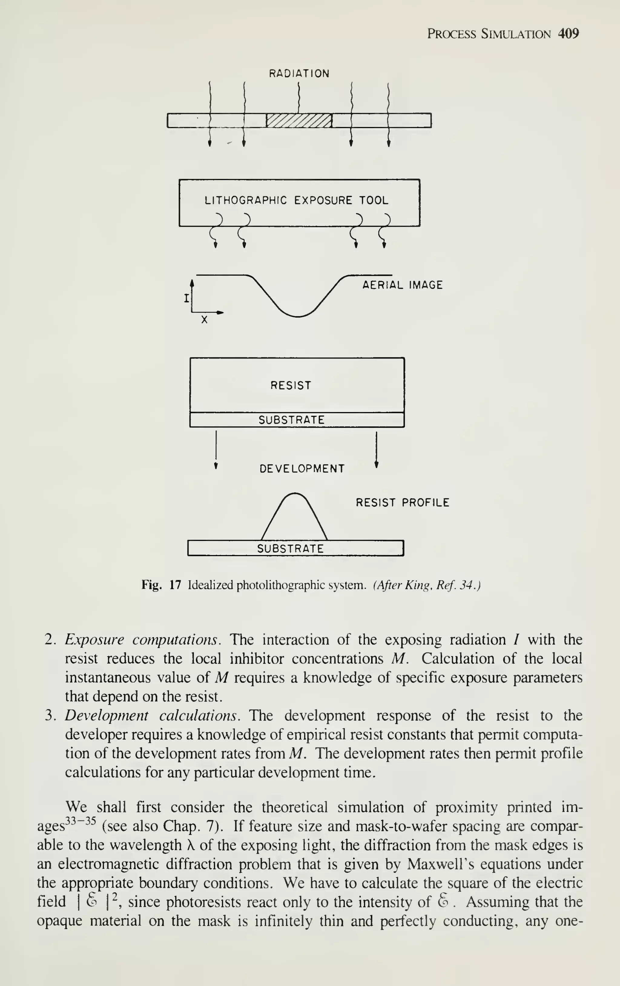
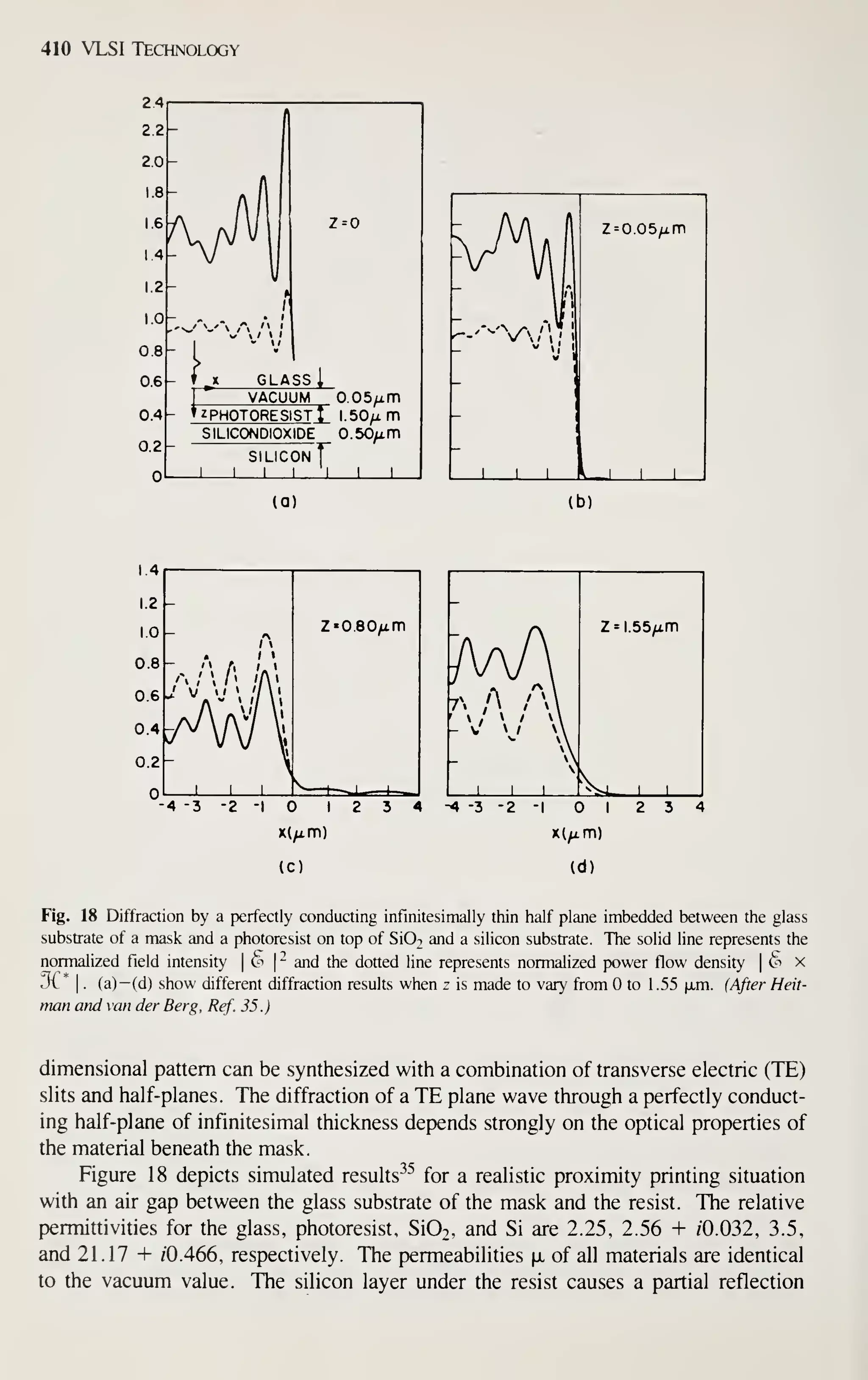
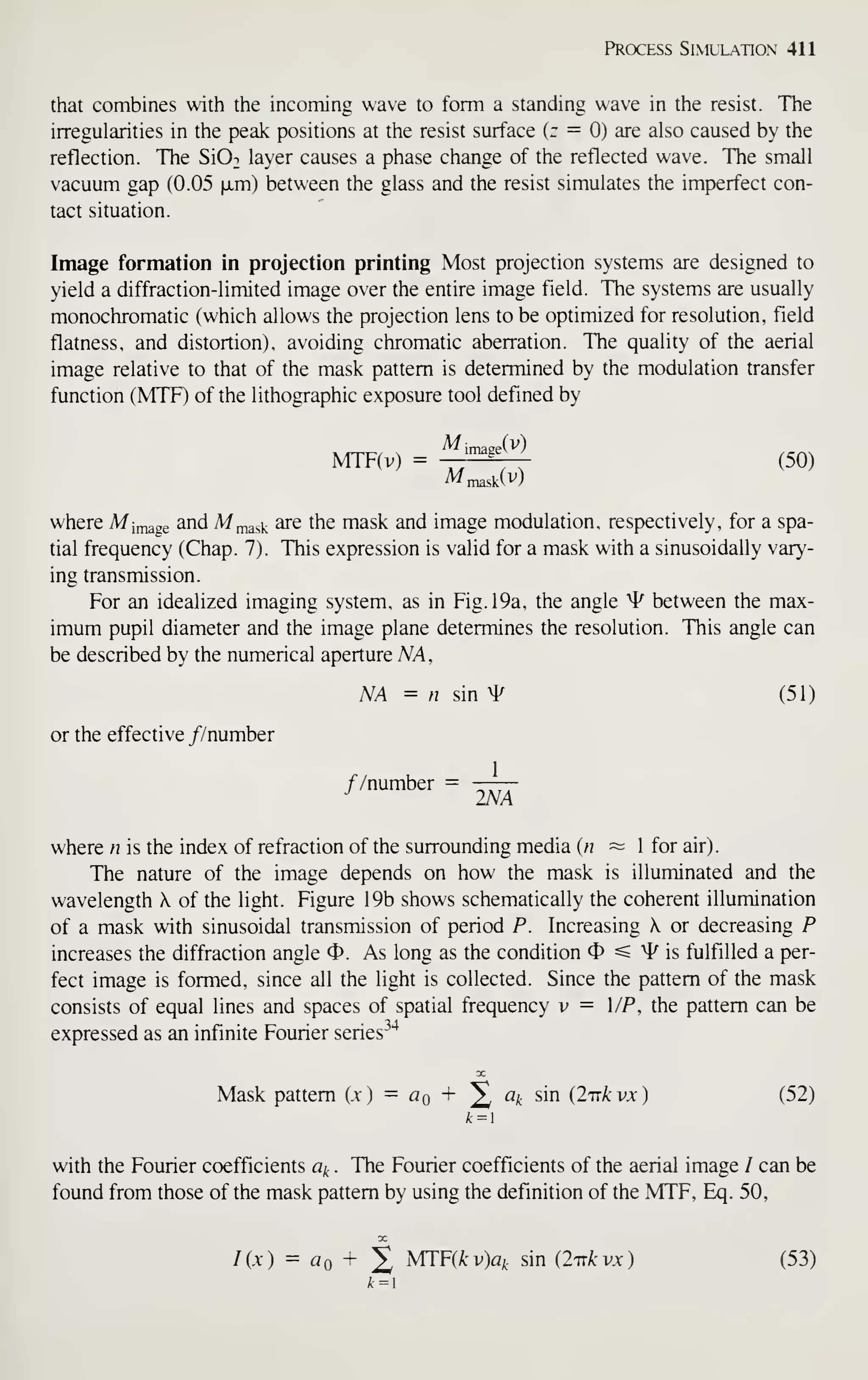
![412 VLSI Technology
OBJECT PLANE
LENS IMAGE PLANE
(a)
MASK
COHERENT
ILLUMINATION
LENS
( + 1)
IMAGE
(-1)
SINUSOIDAL TRANSMITTANCE PERIOD p
(b)
MASK LENS IMAGE
INCOHERENT
(C)
ILLUMINATION
SINUSOIDAL TRANSMITTANCE PERIOD p
Fig. 19 (a) Simple imaging system, (b) Coherent illumination of a mask with sinusoidal transmittance of
period P. (c) Incoherent illumination of a mask with sinusoidal transmittance of period P. (After King, Ref.
34.)
Assuming that the lithographic system operates near its limiting capability, only the
fundamental spatial frequency is important and MTF (kv) = for ^ > 1 . Now we
calculate the amplitude of the aerial image
/I max 4
A(x,z) = —-— sl+ — exp [/c|)(z)] sin (I'ttvx) (54)
with the phase angle 4> describing various aberrations of the optical system. For a
perfect exposure system ^ depends only on the focus condition, given approximately
by
Mz) (55)](https://image.slidesharecdn.com/simonm-220913174129-44ec6f82/75/Simon-M-Sze-editor-Very-Large-Scale-Integration-VLSI-Technology-McGraw-Hill-Inc-US-1983-pdf-432-2048.jpg)
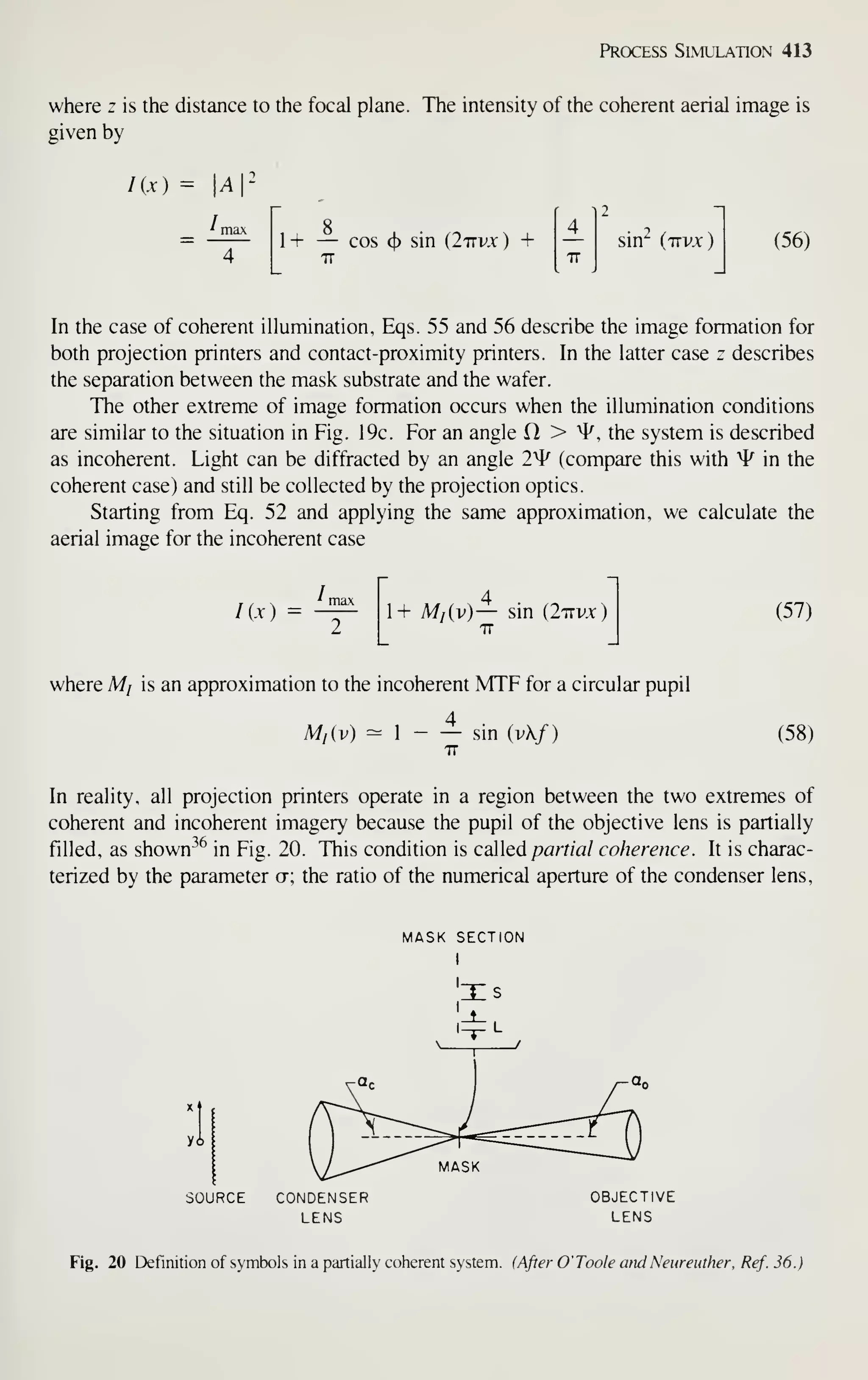
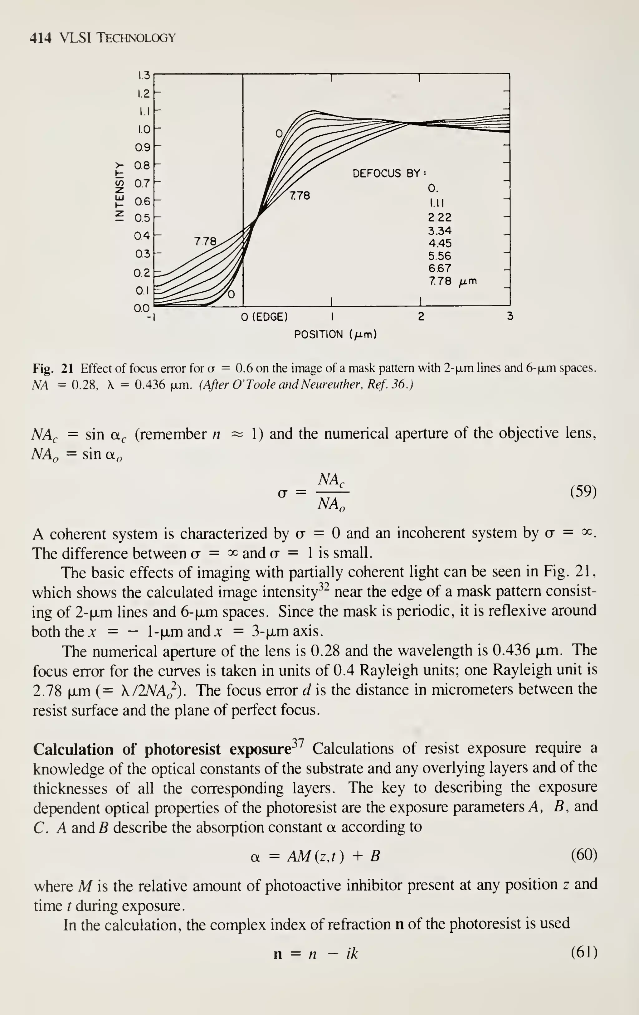
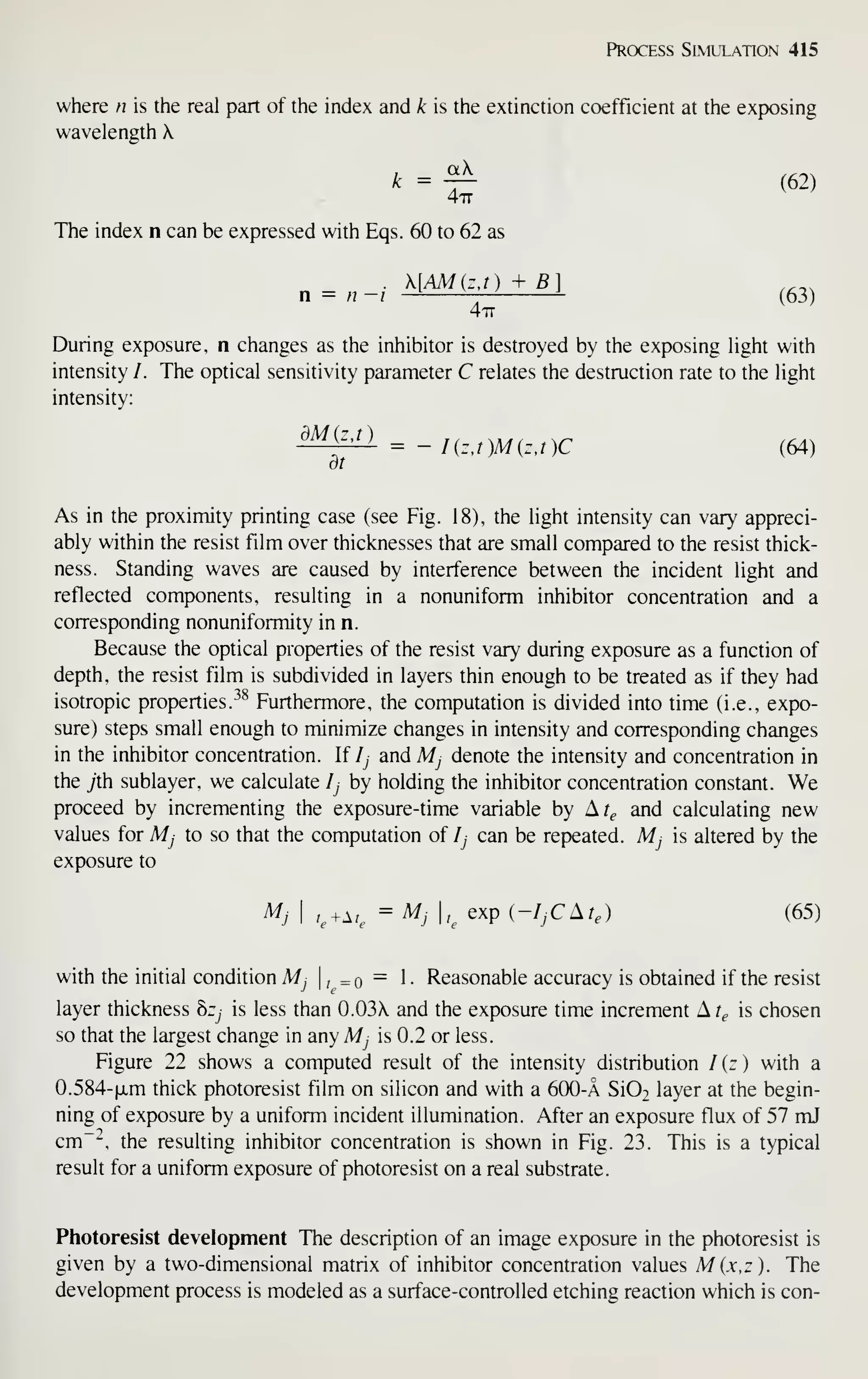
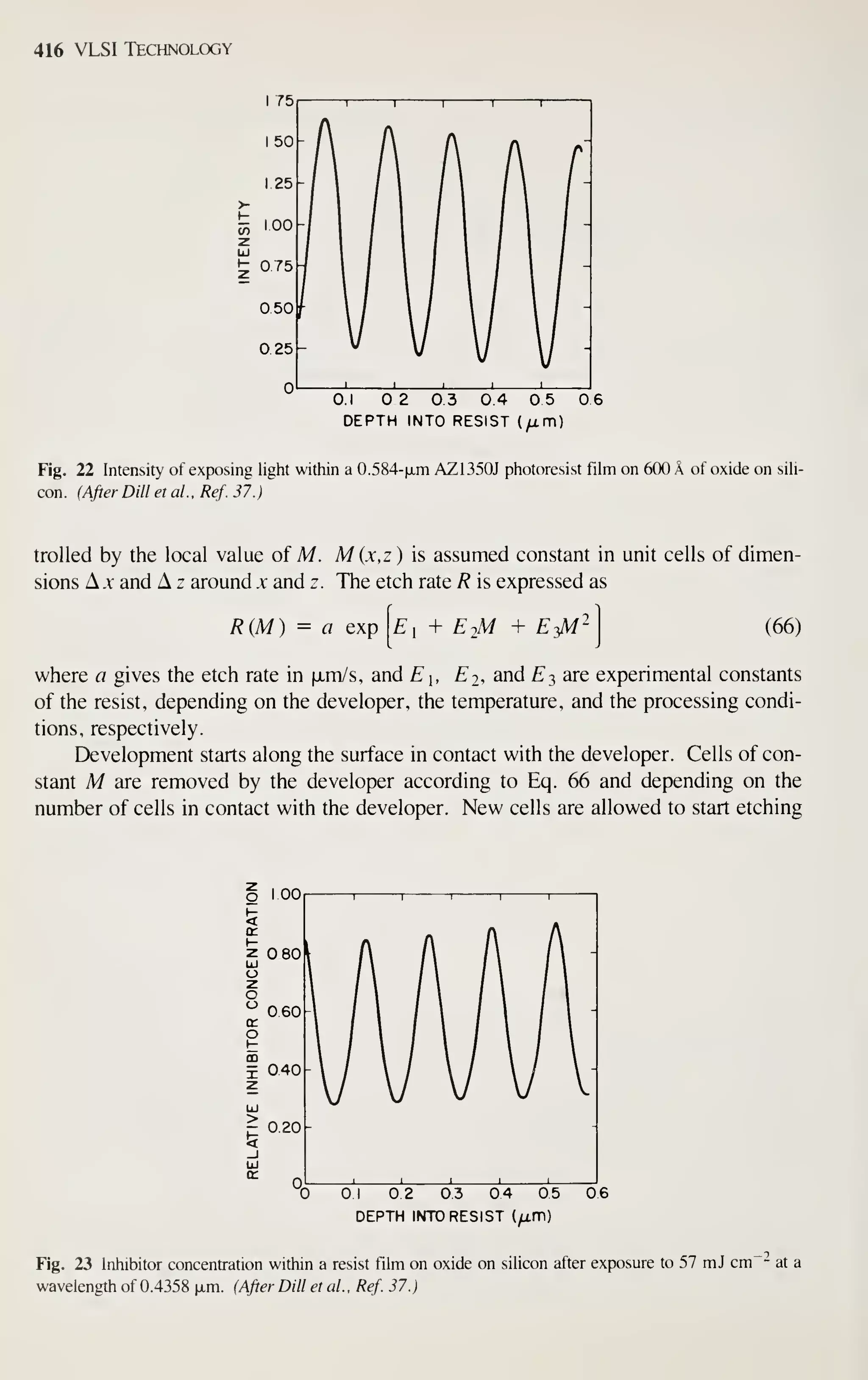
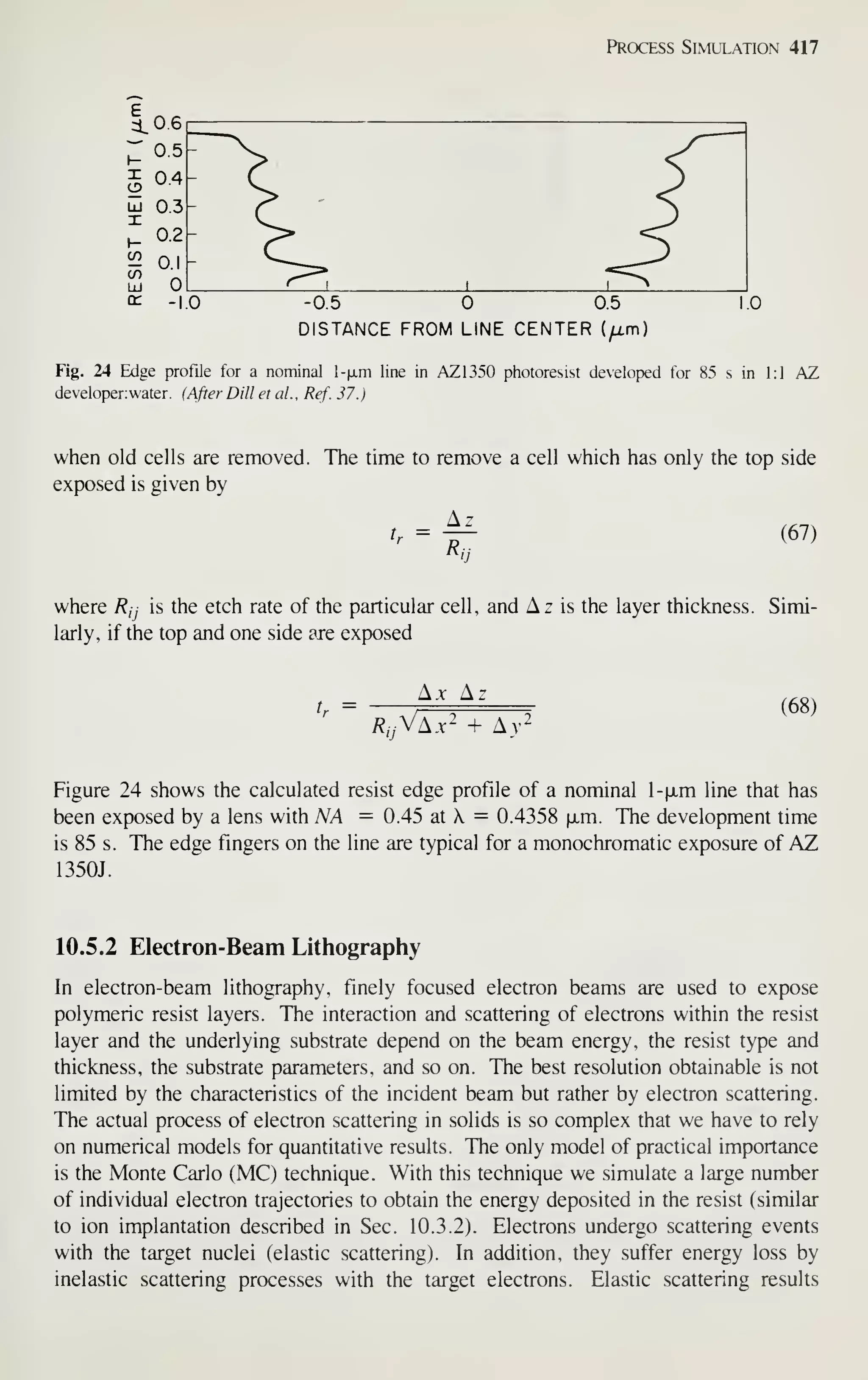
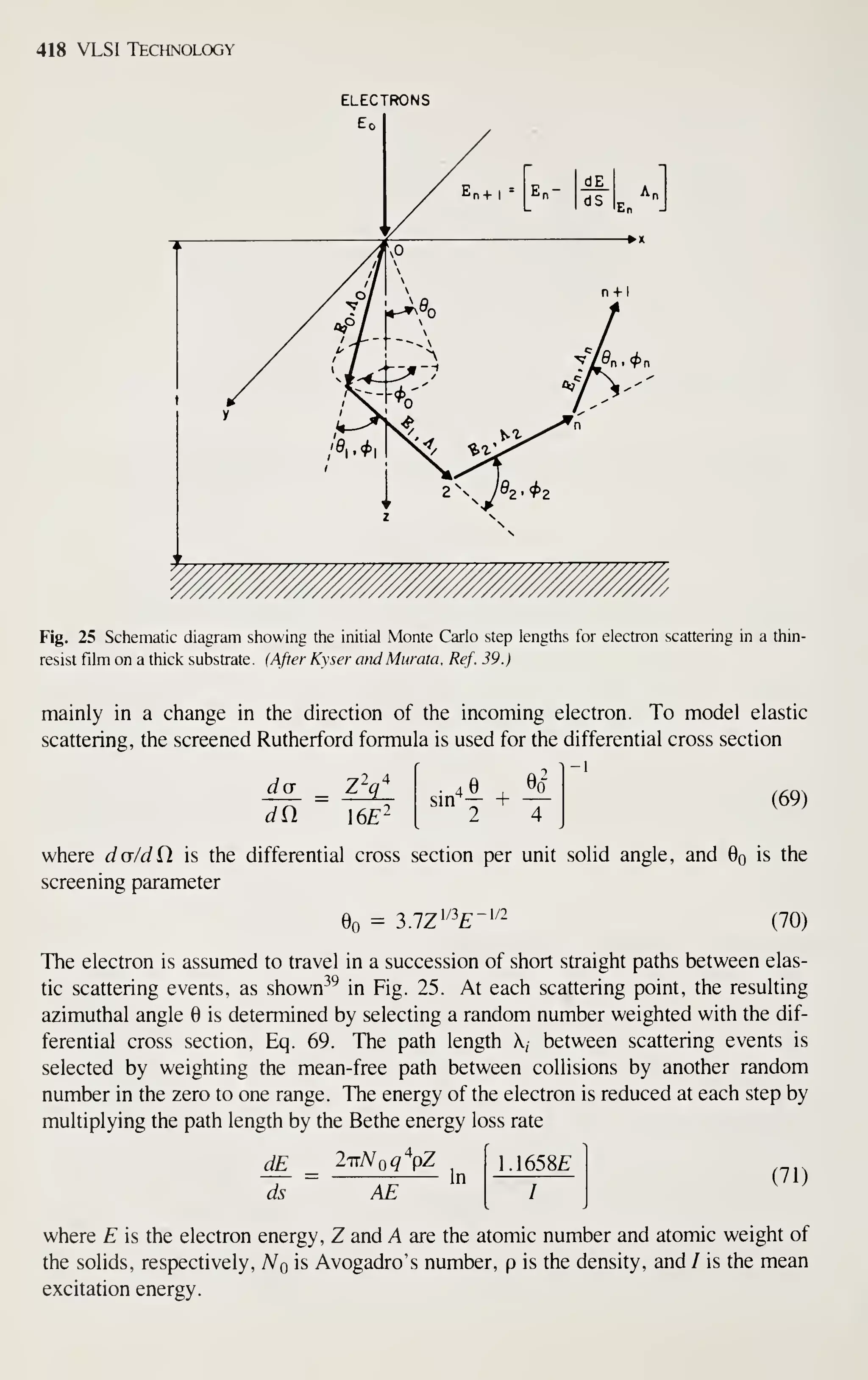
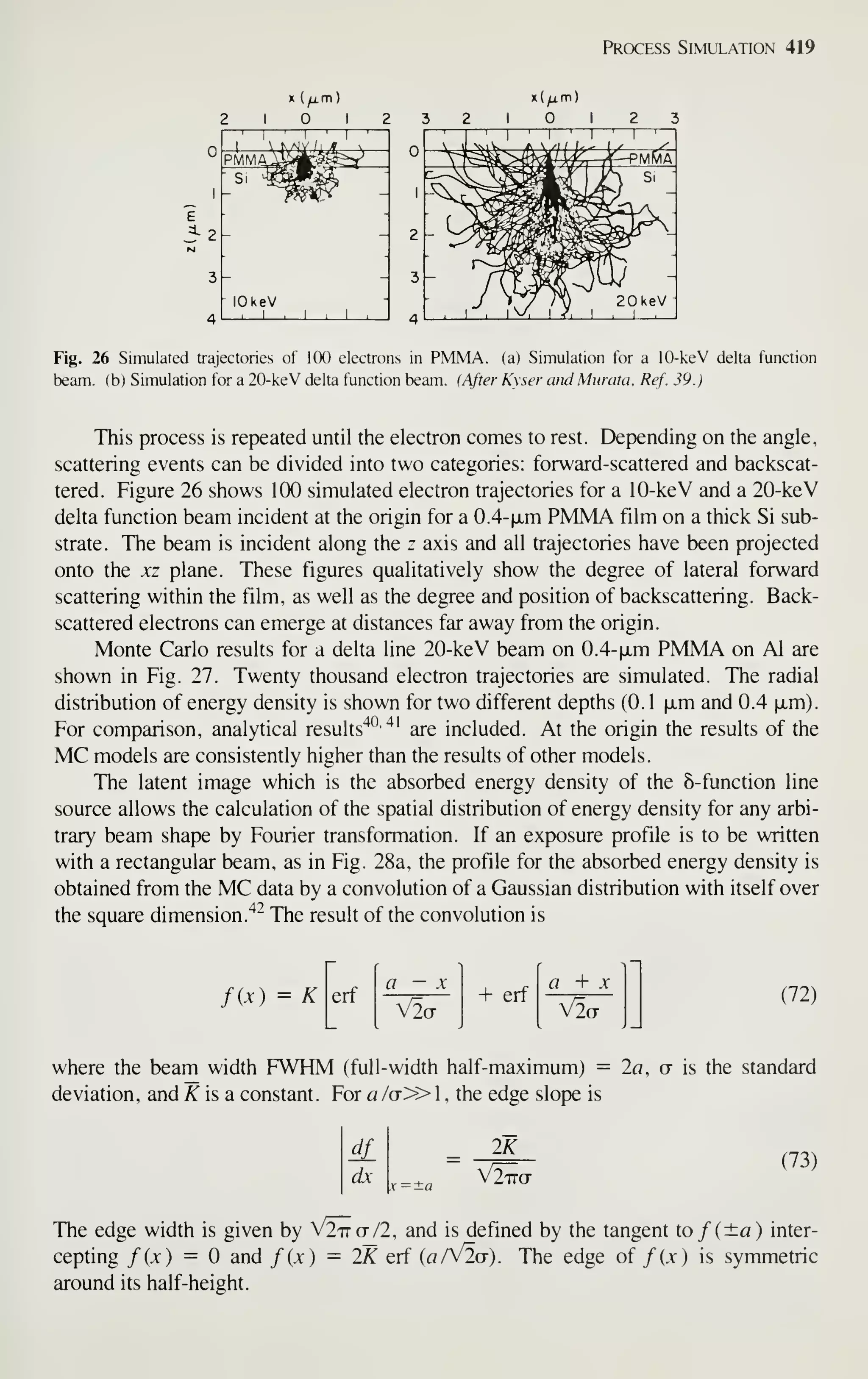
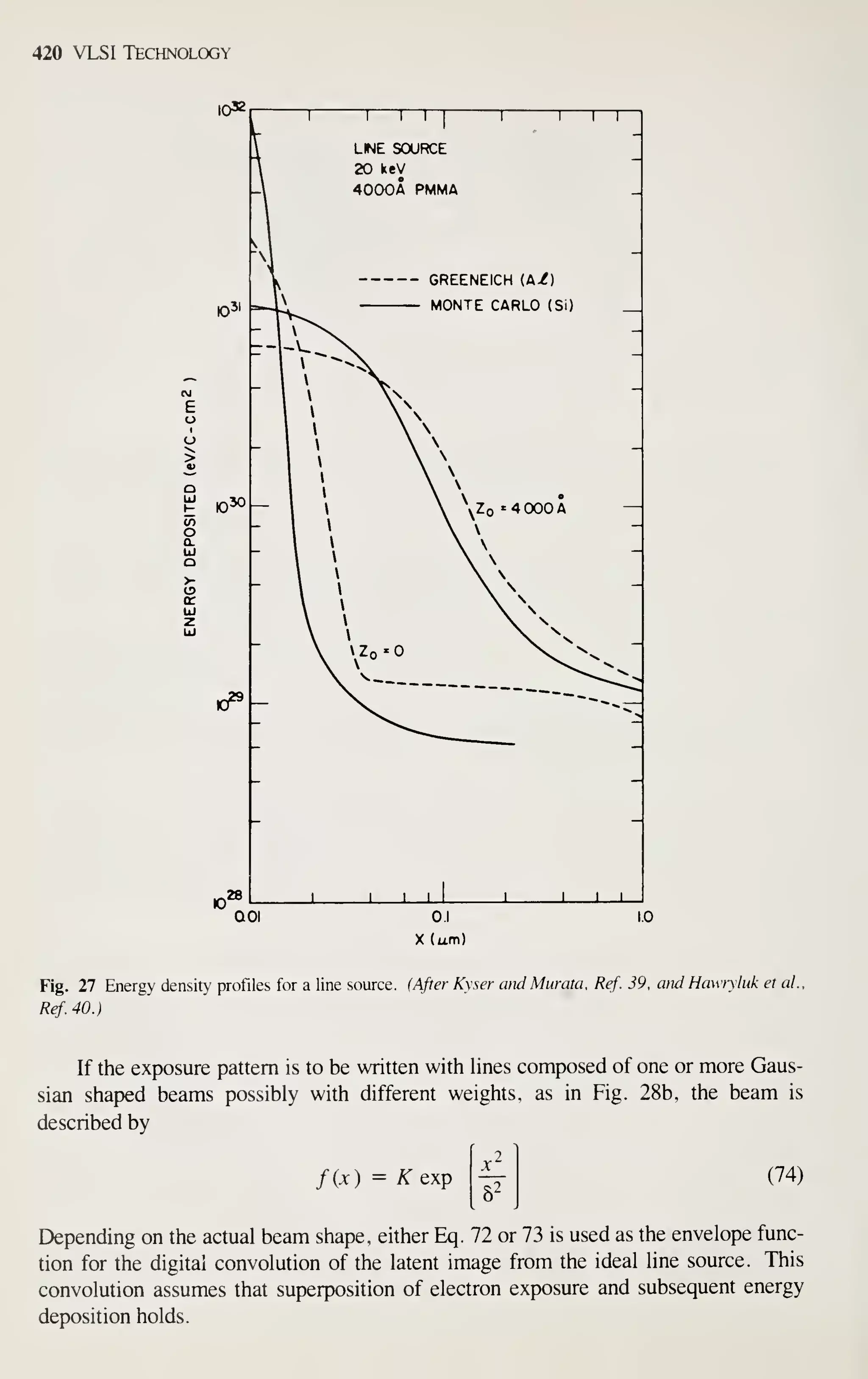
![Process Simulation 421
30-
20
cr=0 25/J.m
FWHM
I
f (MAX)
-f(0)
(a)
F(x) = Ke-''^/S^
(b)
Fig. 28 Exposure patterns for arbitrary beam shapes, (a) Definition of terms. The vertical axis is the
number of electrons distributed over the incident line, normalized to 10^ electrons. (After Kyser and Pyle,
Ref. 42.) (b) Schematic representation of a Gaussian round beam.
Figure 29a shows the simulated MC result of the energy deposited within 1.8 |xm
of resist at three depths for a 25-keV beam. At the surface (z = 0), the distribution is
very narrow, but for increasing depth, it becomes broader due to backscattering con-
tributions from the substrate. To calculate the lateral distribution of deposited energy
(see Fig. 29b), the 5-function distribution is convoluted with the rectangular beam in
Fig. 28a. The energy deposited varies with z. The tails in the original line response
deep in the resist are a significant part of the total distribution in Fig. 29b.
As in optical lithography, we can calculate resist development. For positive
resists, a general relationship between R and E is
R = (A + fi£'')[l-exp i-az)] + e(£) (75)
where R is the etch rate in A/s, z is the distance below the surface, E is the local
absorbed energy density in keV cm~^, and A, fl, and n are appropriate constants.
The dependence of e is modeled as
e(£) = eo + CE"" (76)](https://image.slidesharecdn.com/simonm-220913174129-44ec6f82/75/Simon-M-Sze-editor-Very-Large-Scale-Integration-VLSI-Technology-McGraw-Hill-Inc-US-1983-pdf-441-2048.jpg)
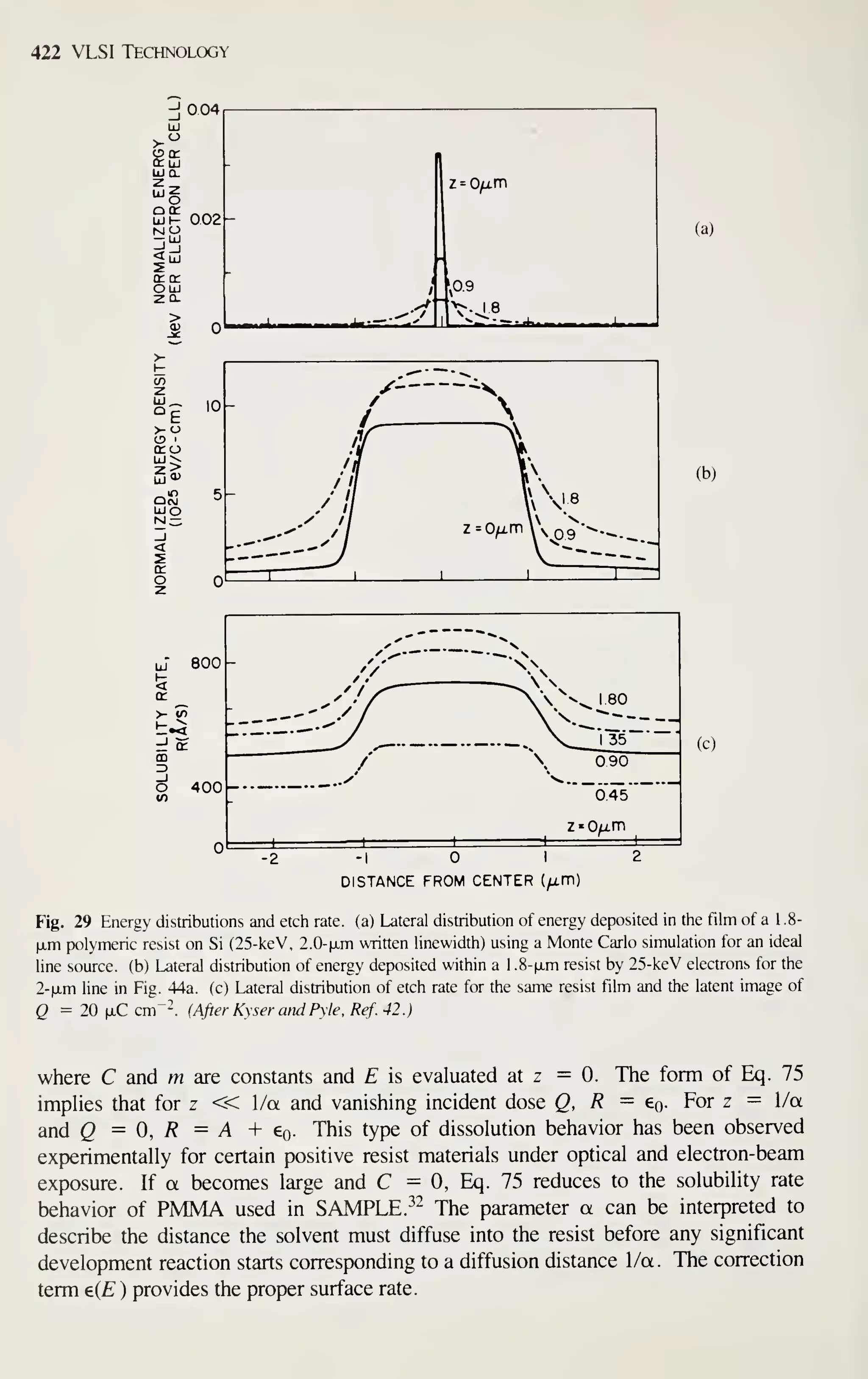
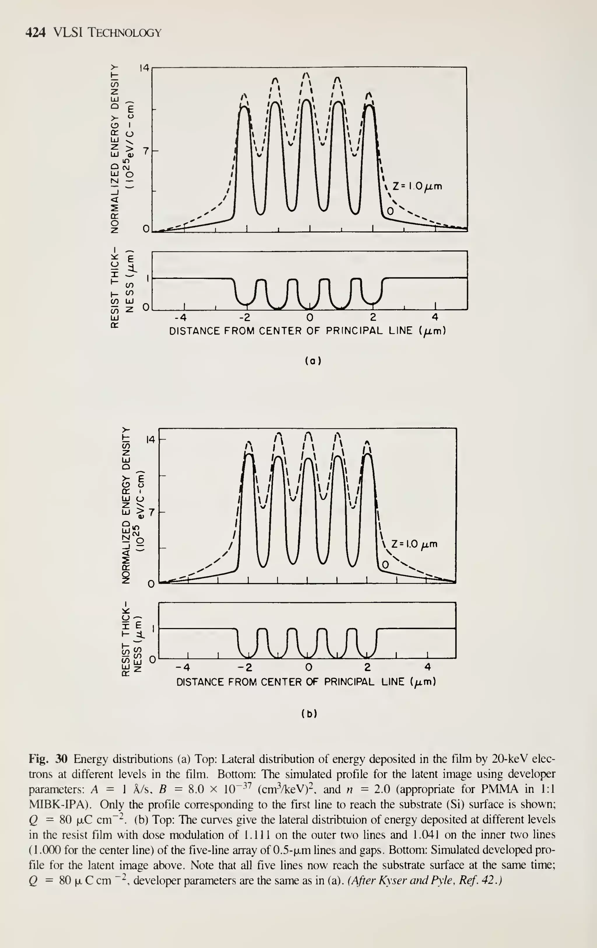
![Process Simulation 425
Fig. 31 Schematic of the proximity function fir ) for arbitrary resist, substrate, and for incident electron
energy. The forward-scattered electron distribution ( ) has a characteristic width Py , while the
backscattered-electron distribution (
) has a characteristic width p^, . (After Parikh. Ref. 45.)
adjustable variable (M = A^)."^^ The single parameter is the primitive figure exposure
£,; the single quantifier M, is the average dose in the primitive figure. Using Eq. 78,
we can calculate the average dose in the jth figure due to exposure of the ith figure:
1
^J A,
(79)
The total average dose in the jth figure is the sum of all contributing component doses
D, = 2^; (80)
where Dp is linear with respect to the exposures and is expressed in the form
Dji = EiKji
and the Kji are symmetric in / and j {Kij =Kji).^
Setting each of the D, equal to some average dose D results in A^ equations
£"1^:11 + £2^12 + + En^in ~ D
E]kj] + EikMj + •••
+ E„kMM — D
li^Nl ni^NN
(81)
(82)
This system can be solved to yield values for all Ej
.
The quality of correction that can be achieved with this algorithm is limited by](https://image.slidesharecdn.com/simonm-220913174129-44ec6f82/75/Simon-M-Sze-editor-Very-Large-Scale-Integration-VLSI-Technology-McGraw-Hill-Inc-US-1983-pdf-445-2048.jpg)
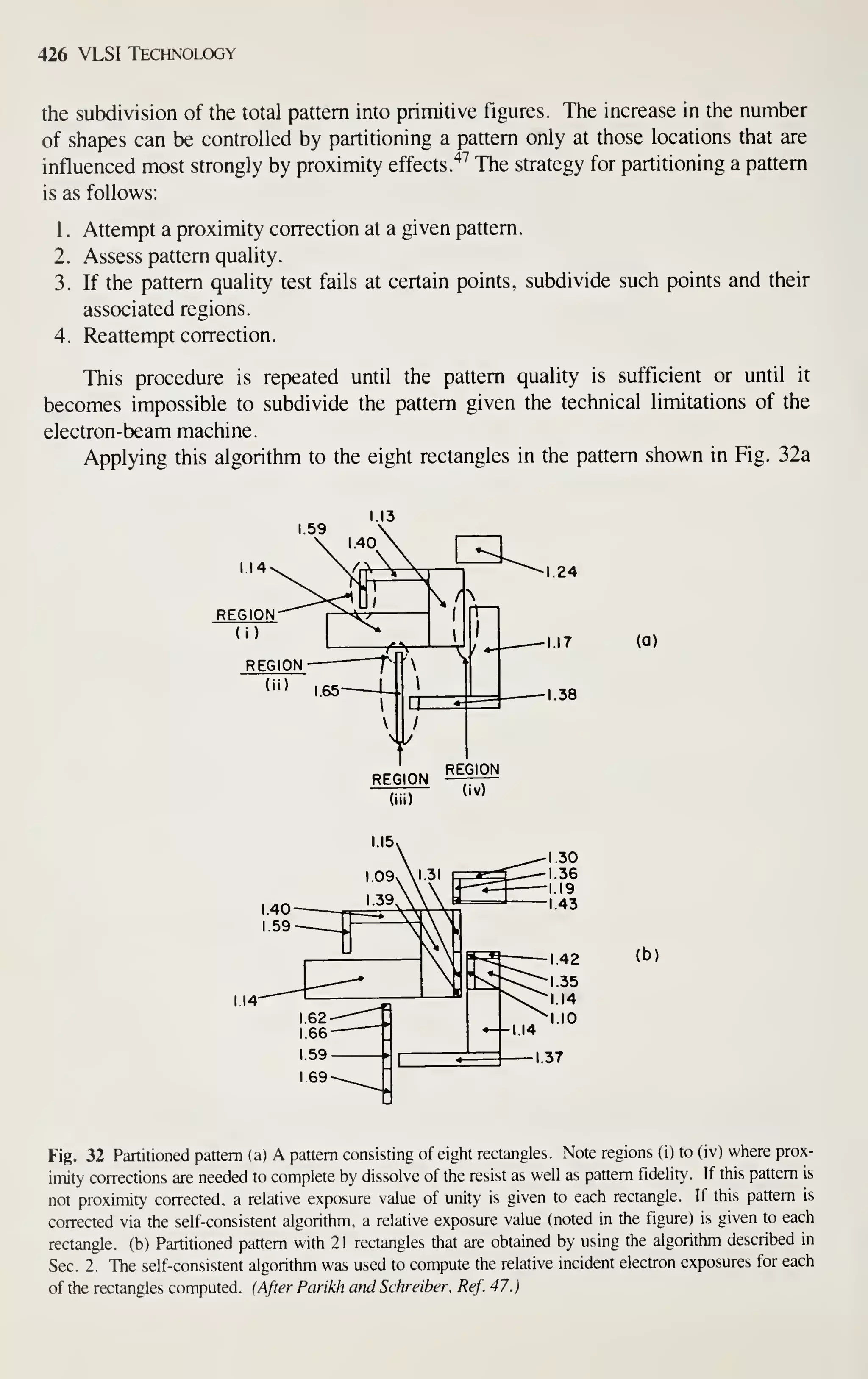
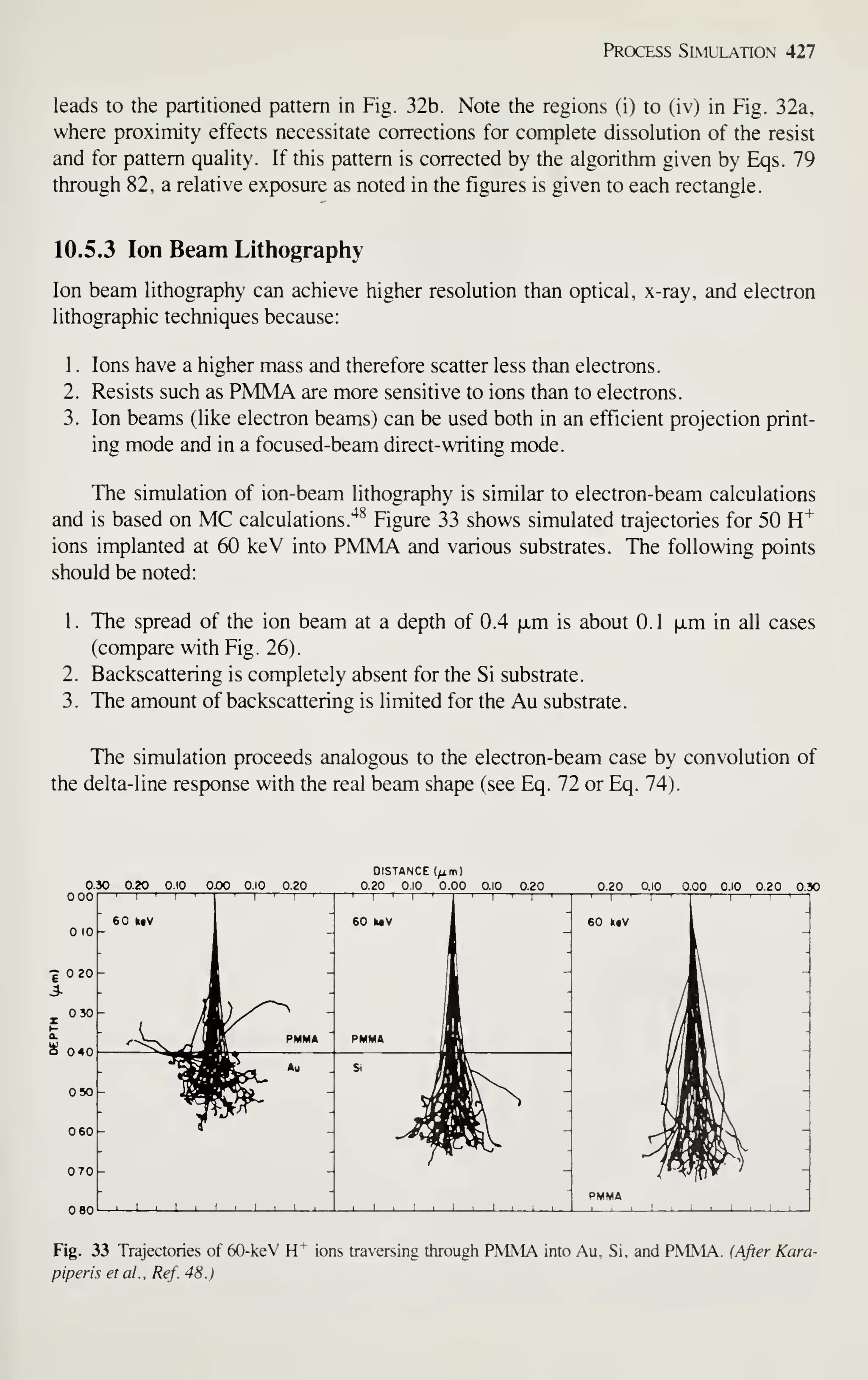
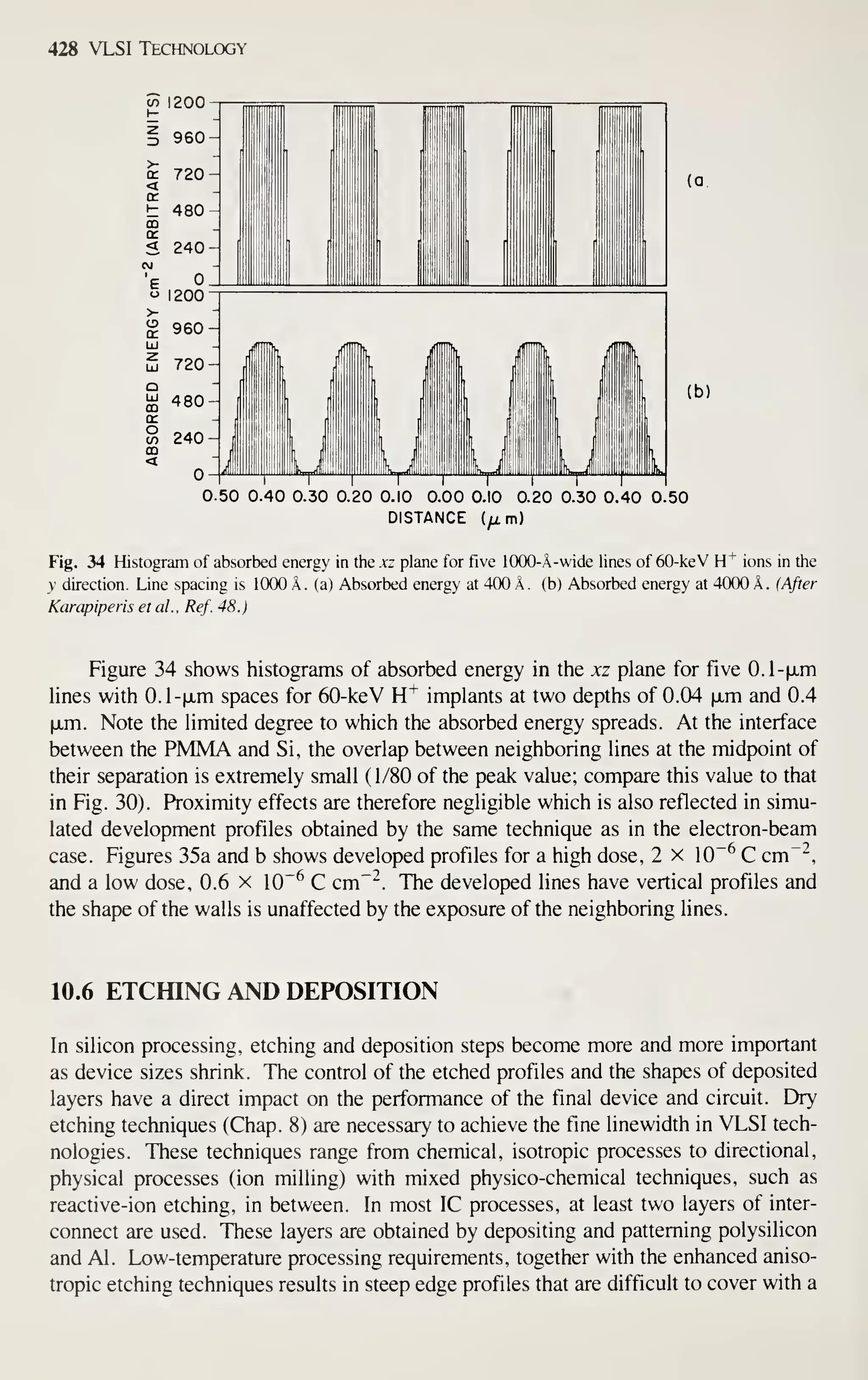
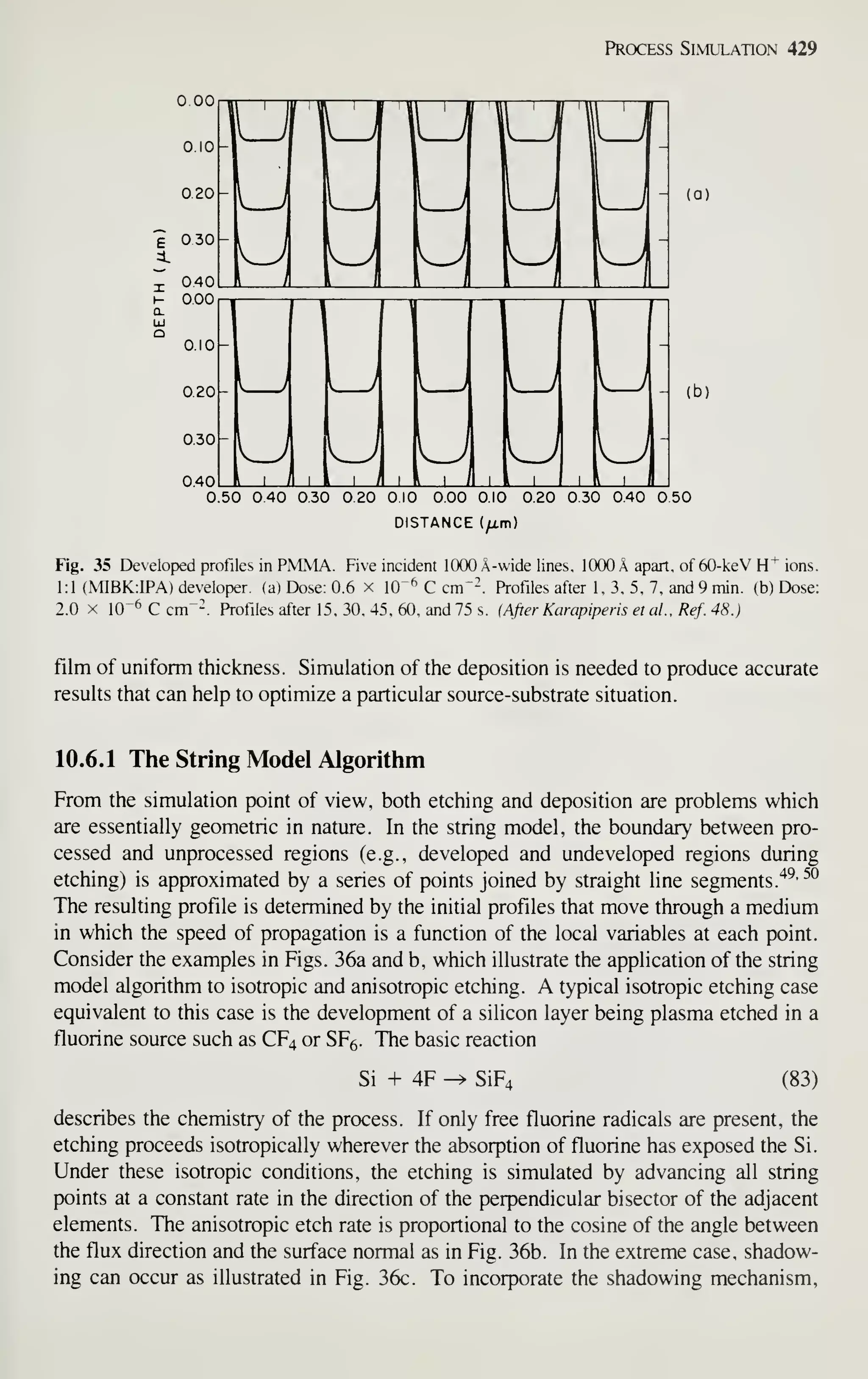
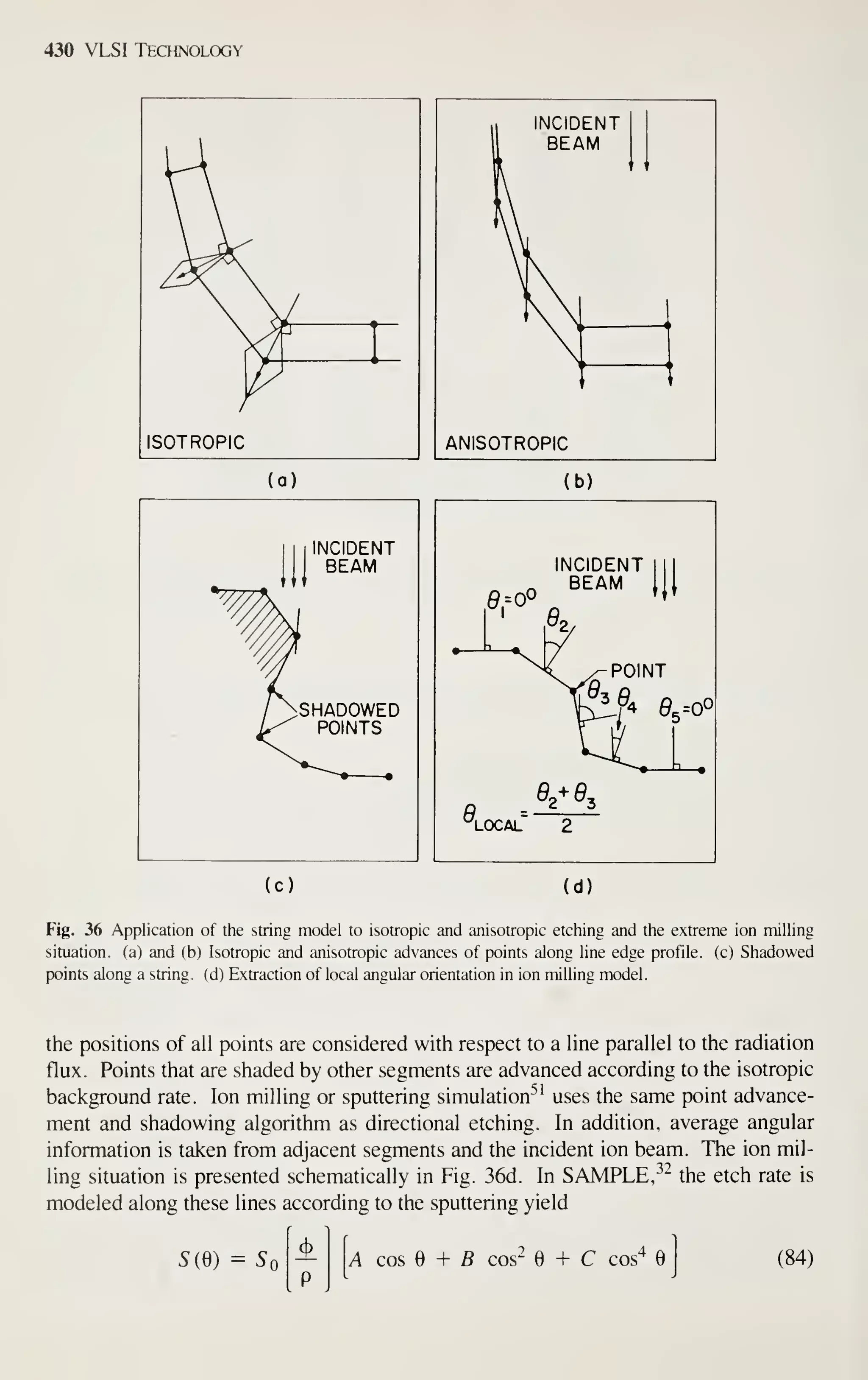
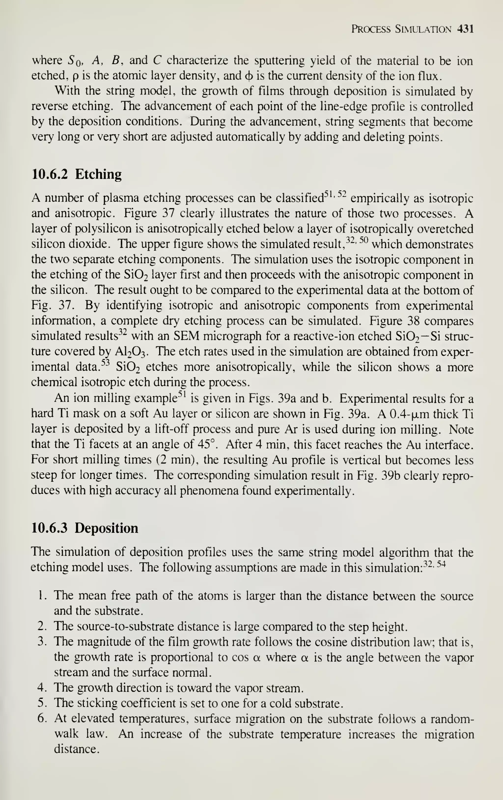
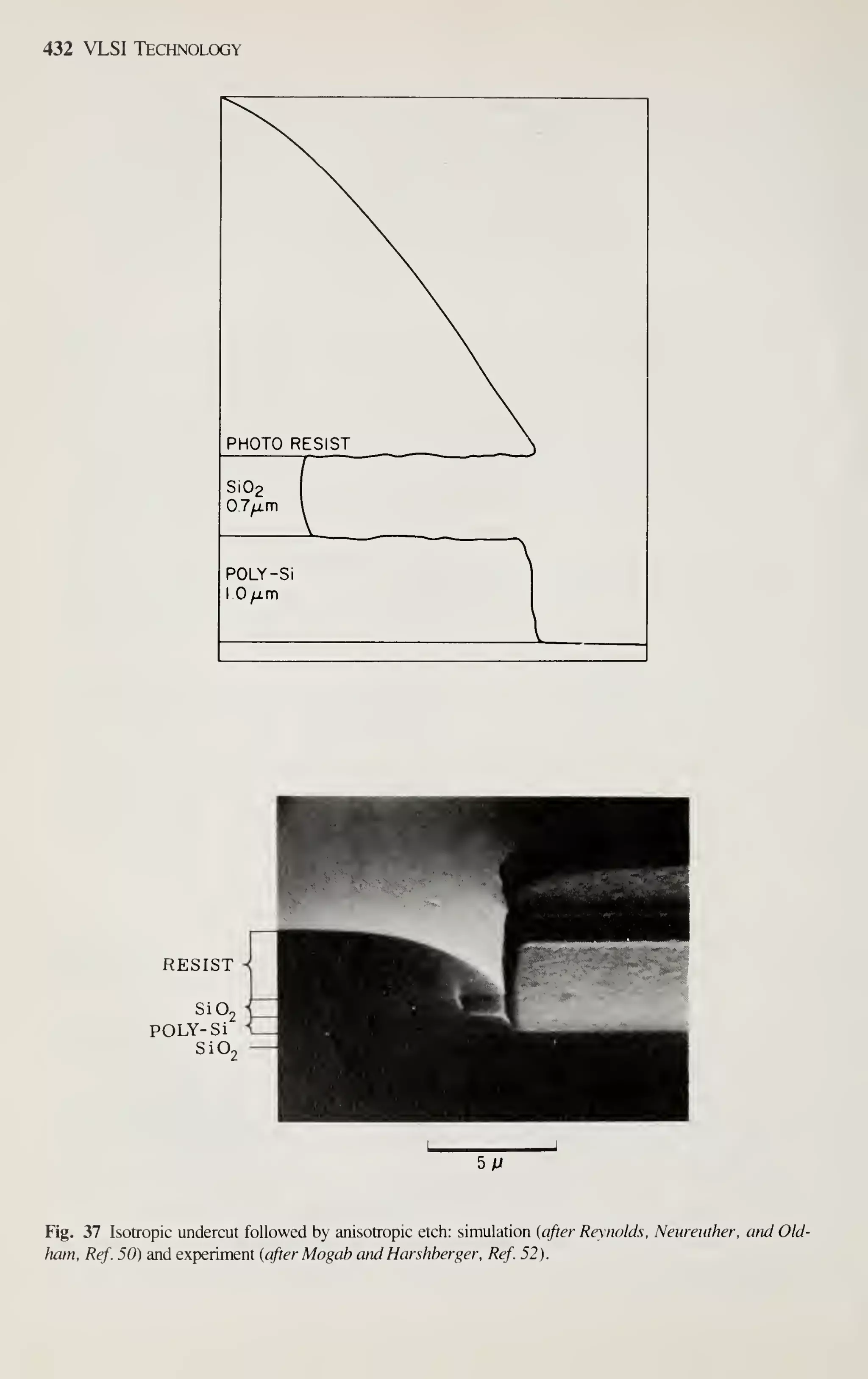
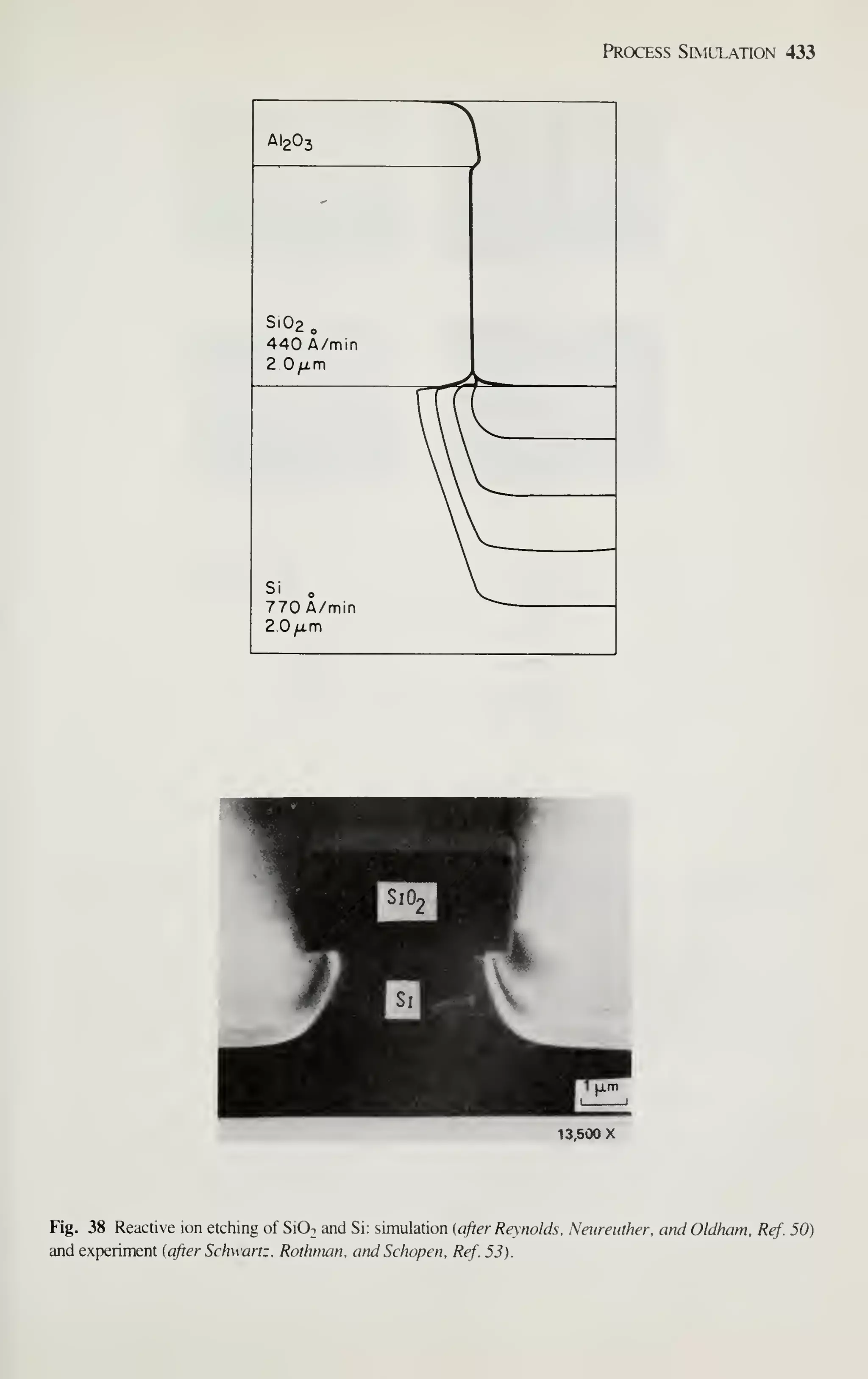
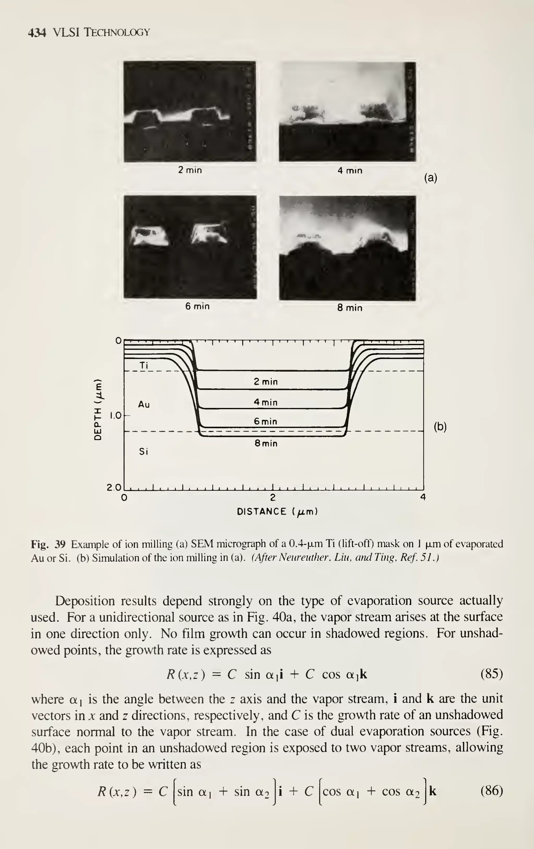
![Process Simulation 435
VAPOR STREAM
U,
SOURCE I
SOURCE 2
.VAPOR STREAM /^
D
IQ
L
r
u,
VAPOR STREAM
(a)
(b)
(c)
Fig. 40 Evaporation sources (a) Unidirectional; (b) dual evaporation; (c) hemispherical.
For a hemispherical source (Fig. 40c) the vapor flux is distributed in a range of direc-
tions with the growth rate
Rix,z) = C cos ai — cos a2 i + C sin a2 — sin aj k (87)
where a] and a2 are the lower and upper bounds of the incident angles of the vapor
streams.
A planetary system is shown in Fig. 41. In this configuration, the rotation of the
planet along the system control axis does not affect the deposition rate. The growth
rate is calculated by holding the planet stationary and rotating only the source along
the planet axis. The growth rate for a deposition from all angles between a^m ^^d
^maY A^
55
RAx,z) = f Ax, (a - p) ^a (88)](https://image.slidesharecdn.com/simonm-220913174129-44ec6f82/75/Simon-M-Sze-editor-Very-Large-Scale-Integration-VLSI-Technology-McGraw-Hill-Inc-US-1983-pdf-455-2048.jpg)
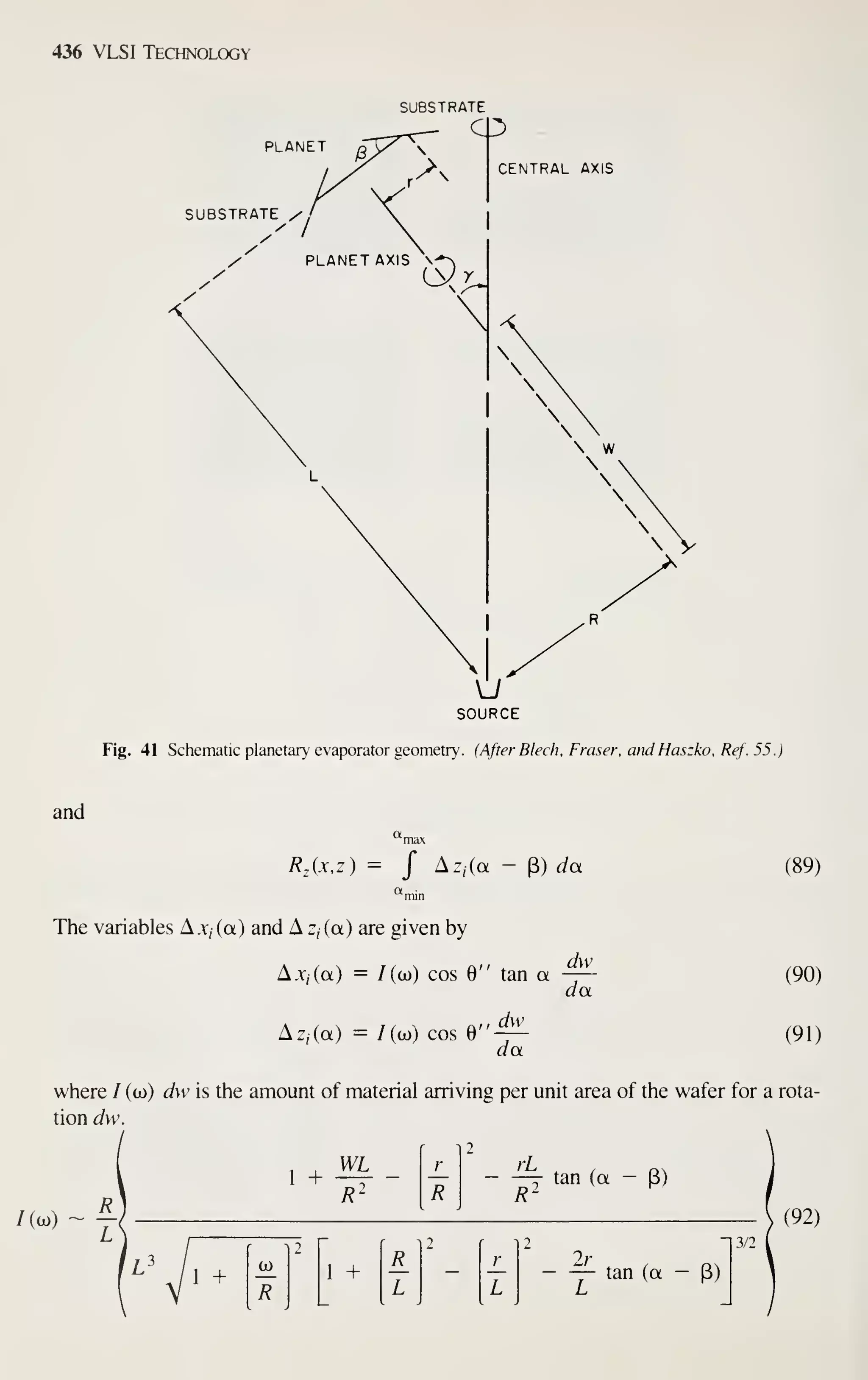
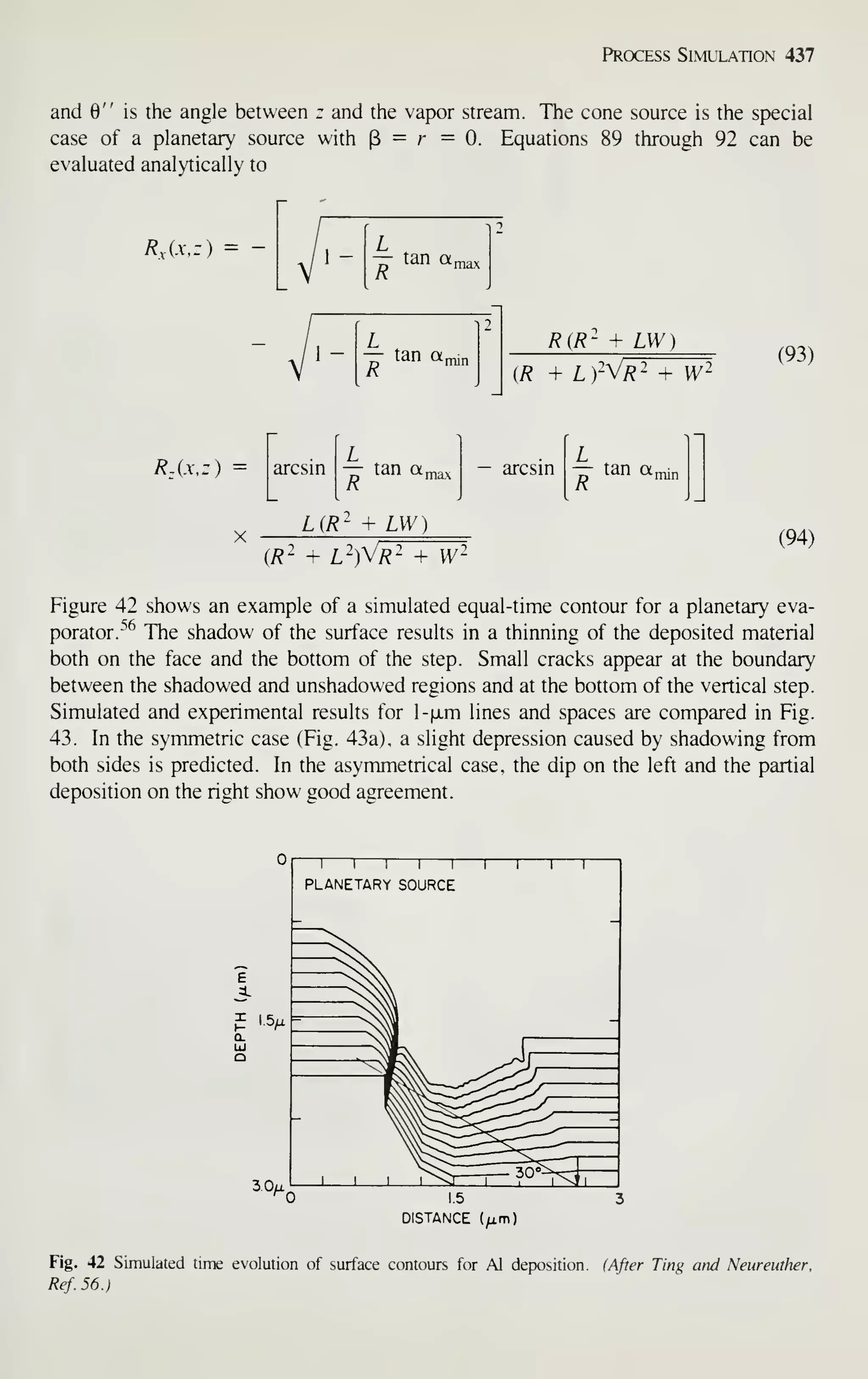
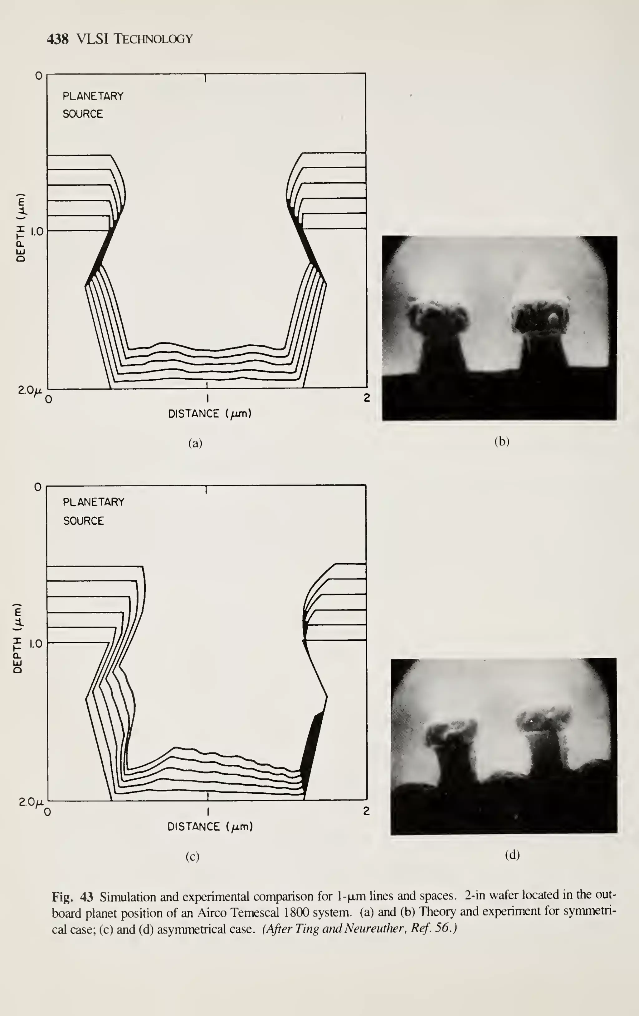
![Process Simulation 439
10.7 DEVICE SIMULATION
For the device design to be successful, process simulation has to be coupled to device
modeling to account for the interrelation between processing and device behavior.
Device modeling is based on the numerical solution of the coupled nonlinear partial
differential equationsr^'' which model the intrinsic behavior of semiconductor devices.
Depending on the problem, one-dimensional''^ or higher-dimensional models^^ are
required. In the following we consider a NMOS process for the fabrication of submi-
crometer size MOSF^Ts.-''^ Electron-beam lithography with a novel multilevel resist
structure defines the pattern. Dry etching techniques transfer the patterns. Table 1
summarizes the wafer process. At all lithographic levels a three-layer resist structure
is used (see Chap. 7). At the bottom is a thick layer of HPR resist followed by a thin
intermediate stencil layer of amorphous silicon and an upper layer of electron resist.
Positive (PBS) and negative resists (GMC) are used at different levels. Apart from
the lithographic steps, the fabrication sequences of major importance are chan-stop
and threshold-adjust implants (steps 3. 5, and 7), and the source-drain formation
implant (step 15).
Several low-temperature (T = 900°C) annealing steps occur in the whole process.
All major process steps have been modeled in two dimensions. Figure 14a shows the
total concentration as calculated by simulating the process in Table 1. Figure 44
Table 1 Wafer process outline
(substrate is 6 to 8 Q-cm. B doped)
1. Grow field oxide, 3500 A
2. Ion implant B. ]50keV.2 x lO'- cm"-
3. Active-area level lithography. PBS( -i-) resist
4. Field oxide etch
5. Ion implant B. 150 keV. 0.5 x lO'- cm"- (optional)
6. Depletion level lithography, PBS( + ) resist
7. Ion implant As. 60 keV, 3 x lO'- cm"-
8. Grow gate oxide. 250 A
9. Deposit polysilicon. 1500 A
10. Polycon level lithography. PBS( + ) resist
11. Etch polysilicon: etch oxide
12. Deposit polysilicon, 2000 A
13. Polysilicon level lithography. GMC( — ) resist
14. Etch polysilicon
15. Ion implant As, 30 keV, 7 x lO'^ cm"-
16. Grow thin oxide, deposit PSG. and planarize
17. Window-level lithography, PBS( + ) resist
18. Etch oxide
19. Form silicide
20. Deposit polysilicon plus Al
21. Metal level lithography, GMC( -) resist
22. Etch Al, etch polysilicon
23. Sinter Al, metallize backside](https://image.slidesharecdn.com/simonm-220913174129-44ec6f82/75/Simon-M-Sze-editor-Very-Large-Scale-Integration-VLSI-Technology-McGraw-Hill-Inc-US-1983-pdf-459-2048.jpg)
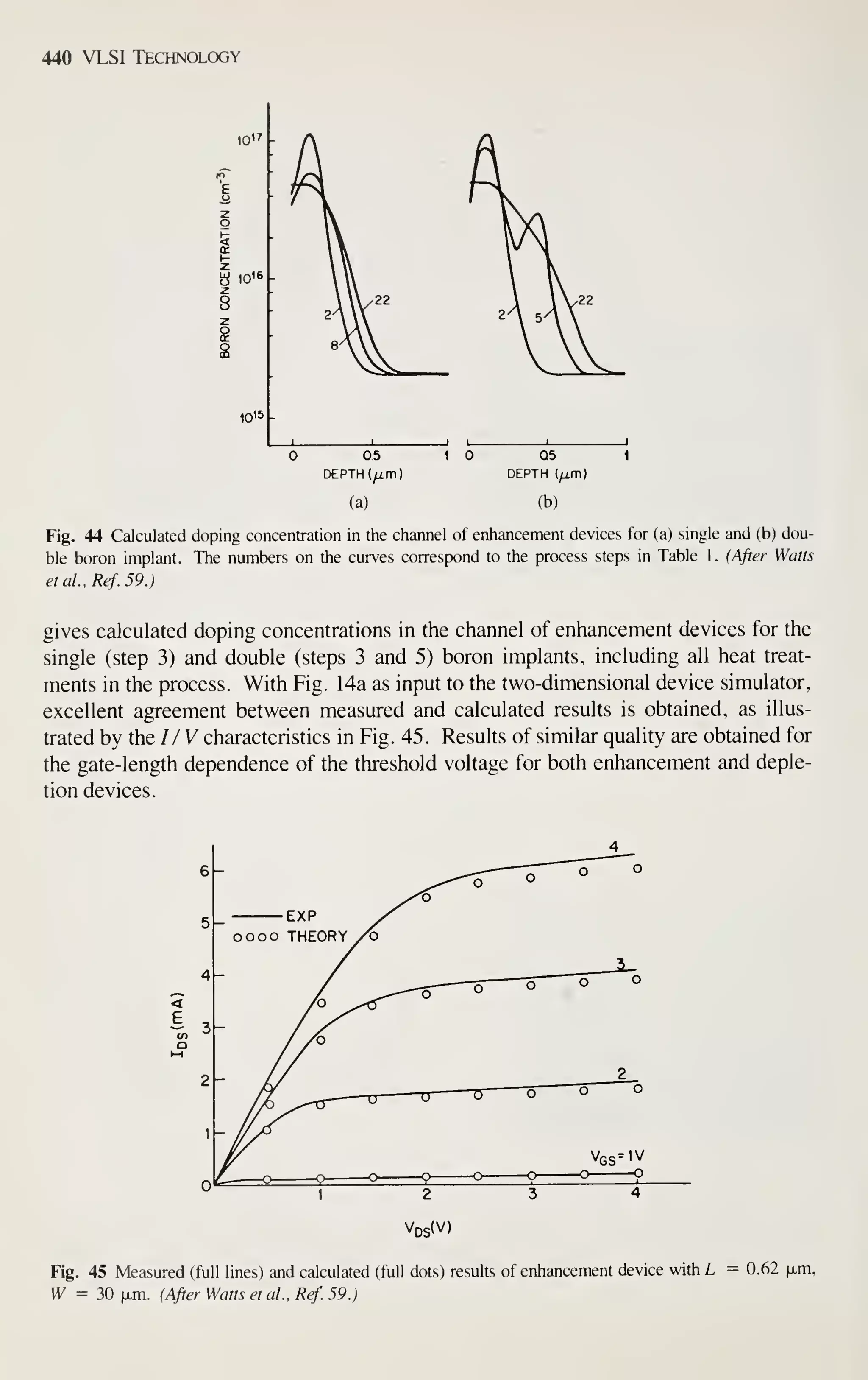
![Process Simulation 441
10.8 SUMMARY AND FUTURE TRENDS
This chapter summarizes the relevant theory and provides examples of process simu-
lation. Theoretical results have been minimized by referencing the important litera-
ture. The material presented, together with the references at the end, should enable
the reader to understand the basic features and goals of process simulation.
Process simulation is a rapidly expanding field and the literature is growing.
With the exception of several theoretical papers, most references cited are from the
late 1970s with the bulk being published in the last few years. We can expect
increased sophistication in computer programs together with an improved understand-
ing of physical processes to take over the job of designing new processes and devices
completely. Optimization of processes will become an automatic tool in the 1980s.
Process and device simulation coupled with circuit simulation will be user-oriented.
In the future, a total design system will allow on-line process design to predict the
desired device and circuit parameter sensitivities, and to facilitate circuit design and
layout with given design rules.
REFERENCES
[1] R. Reif, T. I. Kamins, and K. C. Saraswat, "A Model for Dopant Incorporation into Growing Silicon
Epitaxial Films. I. Theory." 7. Electrochem. Soc, 126, 644 ( 1979).
[2] R. Reif, T. I. Kamins, and K. C. Saraswat, "'A Model for Dopant Incorporation into Growing Silicon
Epitaxial Film. H. Comparison of Theory and Exf)eriment,'" 7. Electrochem. Soc, 126, 653 (1979).
[3] R. Reif and R. W. Dutton, "Computer Simulation in Silicon Epitaxy," J. Electrochem. Soc, 128,
909(1981).
[4] D. A. Antoniadis, S. E. Hansen, and R. W. Dutton, "SUPREM-II-A Program for IC Process Model-
ing and Simulation," Stanford Electronics Laboratories Technical Report No. 5019-2, June 1978.
[5] P. H. Langer and J. I. Goldstein, "Impurity Redistribution during Silicon Epitaxial Growth and Sem-
iconductor Device Processing," J. Electrochem. Soc, 121, 563 (1974); see alsoy. Electrochem. Soc,
124,591(1977).
[6] M. M. Faktor and I. Garrett, Growth of Crystals from the Vapor, Chapman and Hall, New York,
1974.
[7] J. Gibbons, W. S. Johnson, and S. Mylroie, Projected Range Statistics, 2d ed., Wiley, New York,
1975.
[8] B. Smith, Ion Implantation Range Data for Silicon and Germanium Device Technologies, Research
Studies Press. Oregon, 1977.
[9] D. H. Smith and J. F. Gibbons, "Application of the Boltzmann Transport Equation to the Calculation
of Range Profiles and Recoil Implantation in Multilayered Media," in F. Chemow, J. A. Borders, and
D. K. Brice, eds.. Ion bnplantation in Semiconductors 1976, Plenum, New York, 1977.
[10] L. A. Christel and J. F. Gibbons, "An Application of the Boltzmann Transport Equation to Ion Range
and Damage Distributions in Multilayered Targets," 7. Appl. Phys., 51, 6176 (1980).
[11] M. T. Robinson and I. M. Torrens, "Computer Simulation of Atomic Displacement Cascades in
SoUds in the Binary Collision Approximation," Phys. Rev., B9, 5008 (1974).
[12] J. P. Biersack and L. G. Haggmark, "A Monte Carlo Computer Program for the Transport of Ener-
getic Ions in Amorphous Targets," Nucl. lustrum, and Methods, 174, 257 (1980).
[13] S. Kalbitzer and H. Oetzmann, "Ranges and Range Theories," Radiat. Eff., 47, 57 (1980).
[14] W. D. Wilson, L. G. Haggmark, and J. P. Biersack, "Calculations of Nuclear Stopping, Ranges and
Straggling in the Low Energy Region," Phys. Rev., B15, 2458 (1977).](https://image.slidesharecdn.com/simonm-220913174129-44ec6f82/75/Simon-M-Sze-editor-Very-Large-Scale-Integration-VLSI-Technology-McGraw-Hill-Inc-US-1983-pdf-461-2048.jpg)
![Process Simulation 443
[41] J. S. Greeneich. "Electron Beam Processes," in G. R. Brewer ed., Electron-Beam Technology in
Microelectronic Fabrication. Academic, New York, 1980.
[42] D. F. Kyser and R. Pyle, "'Computer Simulation of Electron-Beam Resist Profiles," IBM J. Res.
Develop., 24 A26(19S0).
[43] D. F. Kyser, D. E. Schreiber, C. H. Ting, and R. Pyle, "Proximity Function Approximations for
Electron-Beam Lithography From Resist Profile Simulation," in R. Bakish ed.. Proceedings of the 9th
International Conference on Electron and Ion Beam Science and Technology, The Electrochemical
Society, Princeton, N.J., 1980.
[44] N. D. Wittels, "Fundamentals of Electron and X-Ray Lithography," in R. Newmann ed., Fine-Line
Lithography, North-Holland, New York, 1980.
[45] M. Parikh, "Corrections to Proximity Effects in Electron-Beam Lithography. I: Theory. 11: Implemen-
tation, m: Experiments," y. Appl. Phys.,5(i, 4371, 4378, 4383 (1979).
[46] T. H. P. Chang, "Proximity Effect in Electron-Beam Lithography," J. Vac. Sci. Technol., 12, 1271
(1975).
[47] M. Parikh and D. E. Schreiber, "Pattern Partitioning for Enhanced Proximity—Effect Corrections in
Electron-Beam Lithography," IBM J. Res. Develop., lA, 530 ( 1980).
[48] L. Karapiperis, L Adesida, C. A. Lee, and E. D. Wolf, "Ion Beam Exposure Profiles in PMMA-
Computer Simulation," 7. Vac. Sci. Technol., 19, 1259 (1981).
[49] R. E. Jewett, P. I. Hagouel, A. R. Neureuther, and T. van Duzer, "Line-Profile Resist Development
Simulation Techniques," Polym. Eng. Sci., 17, 381 (1977).
[50] J. L. Reynolds, A. R. Neureuther, and W. G. Oldham, "Simulation of Dry Etched Line Edge Pro-
files," J. Vac. Sci. Technol., 16, 1772 (1979).
[51] A. R. Neureuther, C. Y. Liu, and C. H. Ting, "Modelling Ion Milling," J. Vac. Sci. Technol., 16,
1767(1979).
[52] C. J. Mogab and W. R. Harshberger, "Plasma Processes Set to Etch Finer Lines with Less Undercut-
ting," Electronics, 51, 1 17 (1981).
[53] G. C. Schwartz, L. B. Rothman, and T. J. Schopen, "Competitive Mechanisms in Reactive Ion Etch-
ing in a CF4 Plasma," J. Electrochem. Soc, 126, 464 (1979).
[54] W. G. Oldham, A. R. Neureuther, C. K. Sung, J. L. Reynolds, and S. N. Nandgaonkar, "A General
Simulator for VLSI Lithography and Etching Processes: Part U—Application to Deposition and Etch-
ing," IEEE Trans. Electron Devices, ED-27, 1455 (1980).
[55] I. A. Blech, D. B. Eraser, and S. E. Haszko, "Optimization of Al Step Coverage through Computer
Simulation and Scanning Electron Microscopy," 7. Vac. Sci. Technol., 15, 13 (1978).
[56] C. H. Ting and A. R. Neureuther, "Applications of Profile Simulation for Thin Film Deposition and
Etching Processes," Solid State Technology, 25 (2), 115 (1982).
[57] W. Fichtner and D. J. Rose, "On the Numerical Solution of Nonlinear Elliptic PDEs Arising from
Semiconductor Device Modelling," in M. Schultz, ed., Elliptic Problem Solvers, Academic, New
York, 1981.
[58] D. C. D'Avanzo, M. Vanzi, and R. W. Dutton, "One-Dimensional Semiconductor Device Analysis
(SEDAN)," Stanford Electronics Laboratories Technical Report No. 6-201-5, October 1979.
[59] R. K. Watts, W. Fichtner, E. Fuls, L. R. Thibault, and R. L. Johnston, "Electron-Beam Lithography
for Small MOSFETs," IEEE Trans. Electron Devices, ED-28, 1338 ( 1981).
[60] E. H. Nicollian and J. R. Brews, MOS (Metal Oxide Semiconductor) Physics and Technology, Wiley,
New York, 1982.
PROBLEMS
1 Diffusion from a growing epitaxial layer into an undoped substrate.
Consider the case of an undoped silicon substrate. Suppose we deposit an epitaxial layer with concen-
tration Cq on top of this substrate. Since epitaxial deposition temperatures are usually high, impurities will
diffuse out of the depositing layer into the substrate and vice versa. For a one-dimensional geometry, solve
the diffusion equation.](https://image.slidesharecdn.com/simonm-220913174129-44ec6f82/75/Simon-M-Sze-editor-Very-Large-Scale-Integration-VLSI-Technology-McGraw-Hill-Inc-US-1983-pdf-463-2048.jpg)
![444 VLSI Technology
2 Diffusion from a doped substrate into an undoped epitaxial layer.
This case concerns putting an undoped layer on a homogeneously doped semi-infinite substrate. The
problem is more difficult than Prob. 1 . because we have to incorporate the fact that some of the dopant that
diffuses into the layer out of the substrate diffuses straight through and evaporates from the growth surface.
A net loss of dopant occurs if the rate that dopant atoms leave the surface at z = is greater than the rate at
which they join it from the ambient atmosphere. For a one-dimensional geometry, solve the diffusion equa-
tion incorporating the evaporation case.
3 Solve the scattering integral
= IT — 2/?
dr
(1)
V{r]
for a repulsive Coulomb potential V (r ) = C/r (Cj >0). Calculate the differential cross section
a(e)
dp
sin ^e
(2)
4 Write a FORTRAN program to calculate Pearson IV distributions.
5 Most frequently, the semiconductor substrate is subjected to a heat cycle after the implantation step, and
the impurities are redistributed. Near the mask edge, this redistribution is obtained by solving the two-
dimensional diffusion equation
dC
= D (1)
assuming intrinsic diffusion conditions. Calculate the analytical solution for the following initial condition
(i.e., profile after implantation)
C{x,z,t = (b)
= C^ [c^Cr.z.r = 0) + CR(x,z,t = 0)
]
where C ^^ is the peak concentration and
Ci^ixj.O) = — exp
2A/?;
erfc
V2AX
(2)
(3)
A/?„
'^'^''''' =
lVto''''
(a„.v + z - R')-
2Dr
1 + erf
-V ^Rp ajz - Rp) AX-
AX AR„
(4)
and
Do = A^/ + a^ AX2 (5)
a^ = tan gives the edge slope of the mask, and ^^ , A/?^ , and AX are the usual Gaussian parameters.
6 Derive Eqs. 93 and 94 for the deposition rates of a cone source.
7 Solve the diffusion problem of redistributing donor and acceptor impurities between Si and Si02 during
thermal oxidation at high temperature. Assume that the initial impurity distribution in the silicon is uniform.
8 Same as Prob. 7, but for a nonuniform initial impurity distribution. Use the method of finite differences
to discreti2e the diffusion equation.](https://image.slidesharecdn.com/simonm-220913174129-44ec6f82/75/Simon-M-Sze-editor-Very-Large-Scale-Integration-VLSI-Technology-McGraw-Hill-Inc-US-1983-pdf-464-2048.jpg)
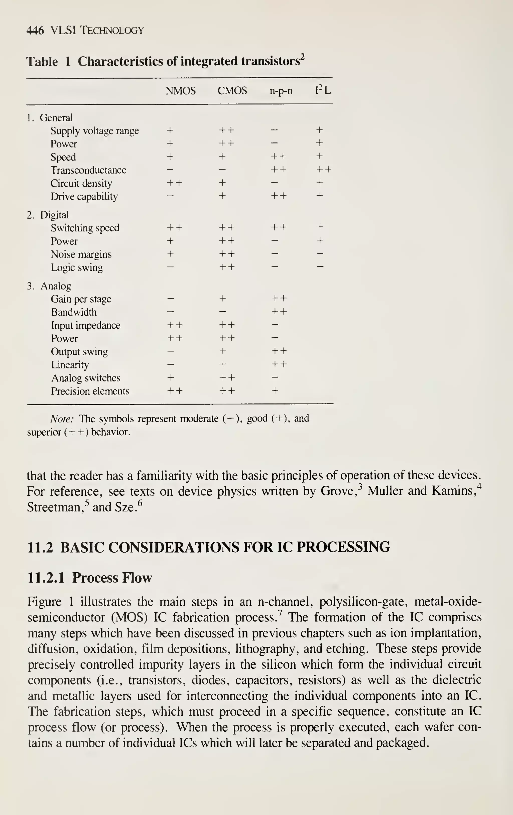
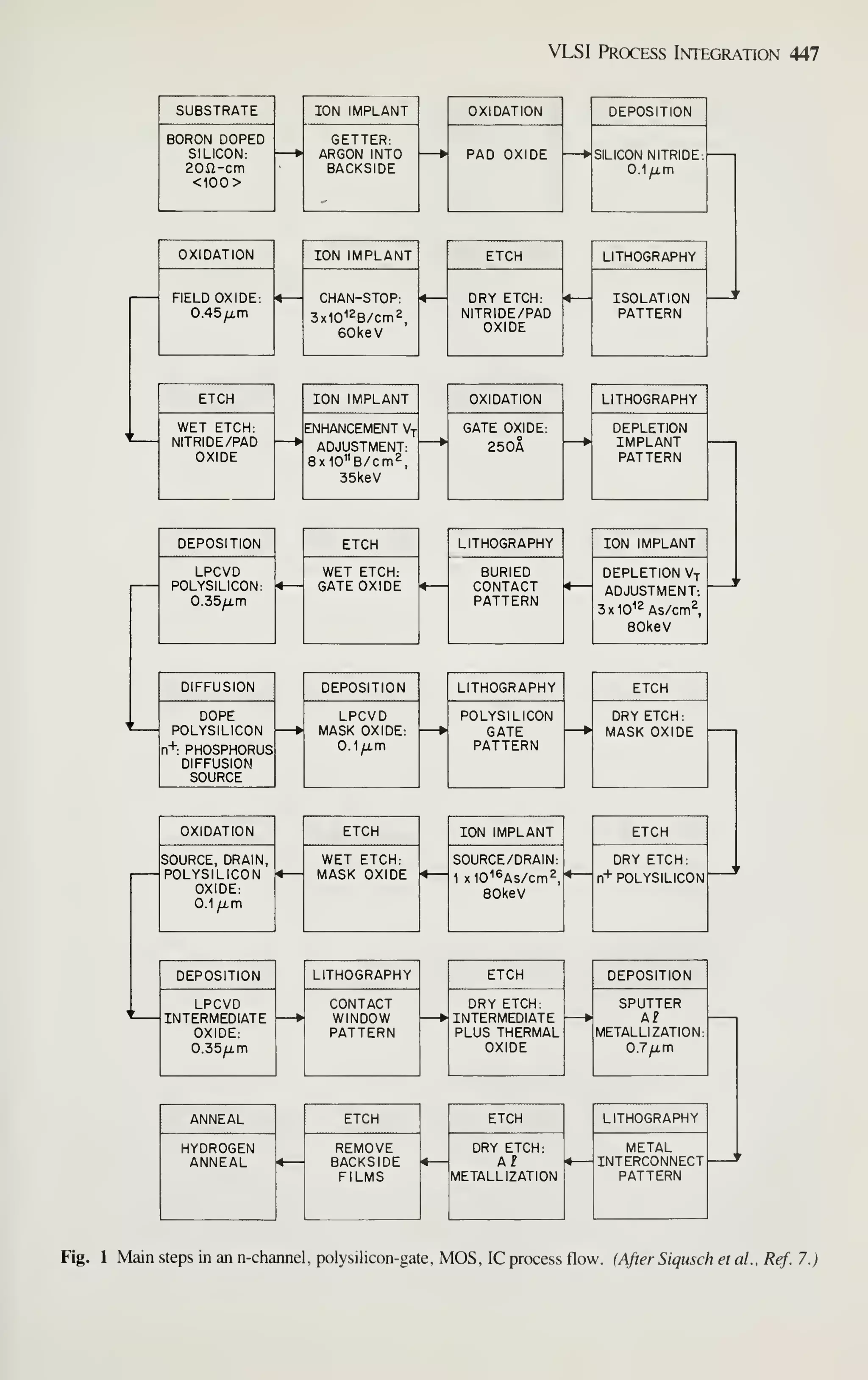
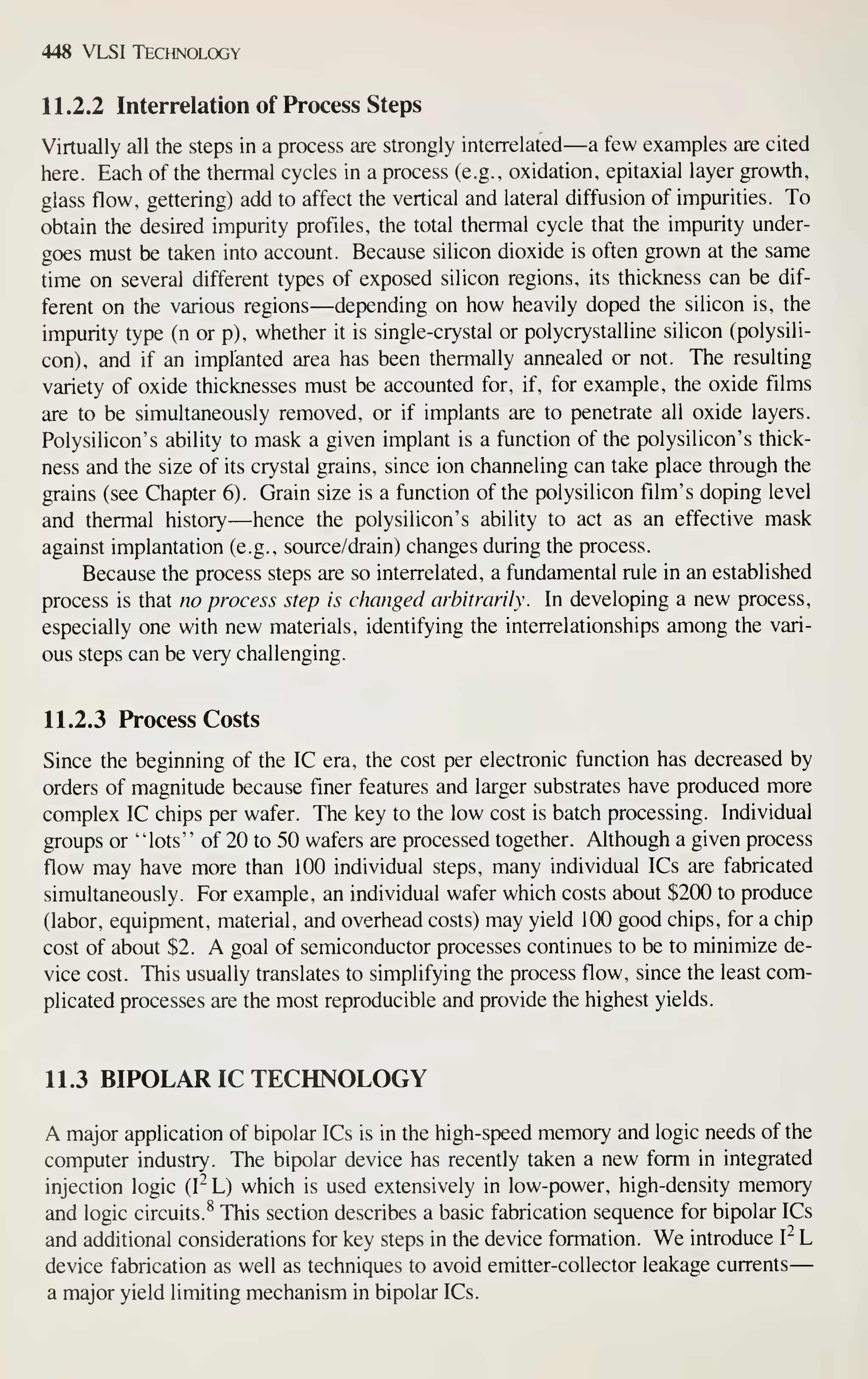
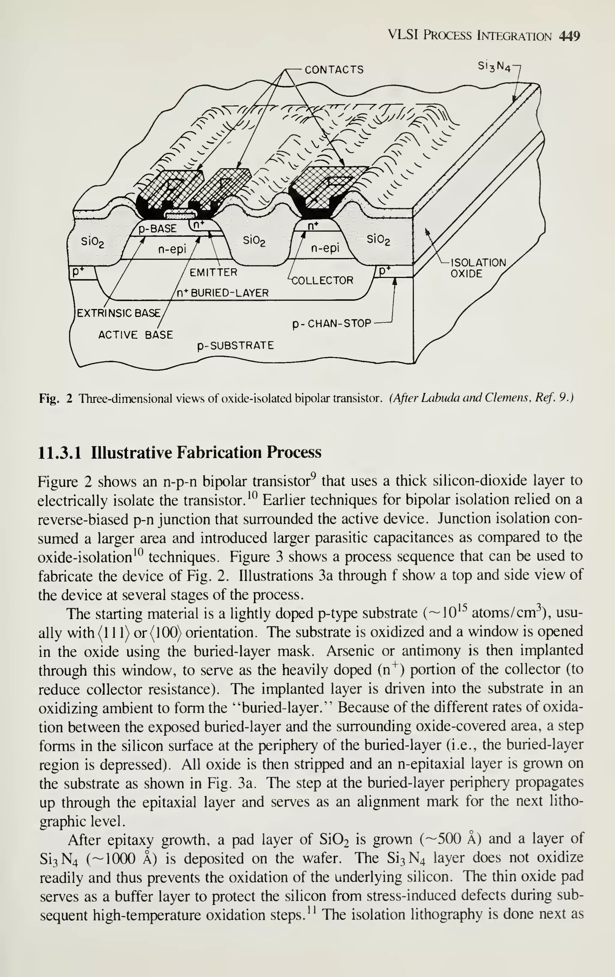
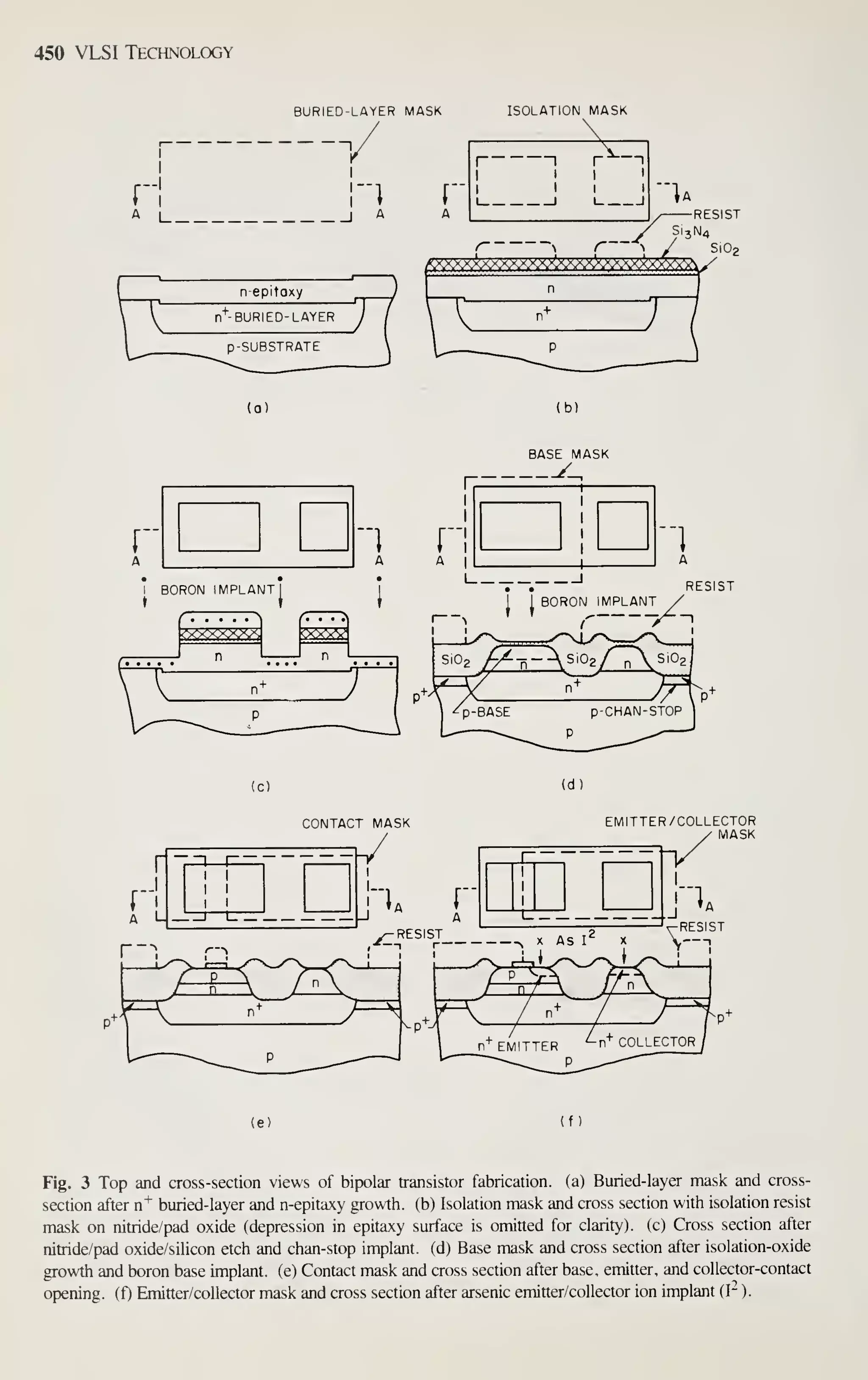
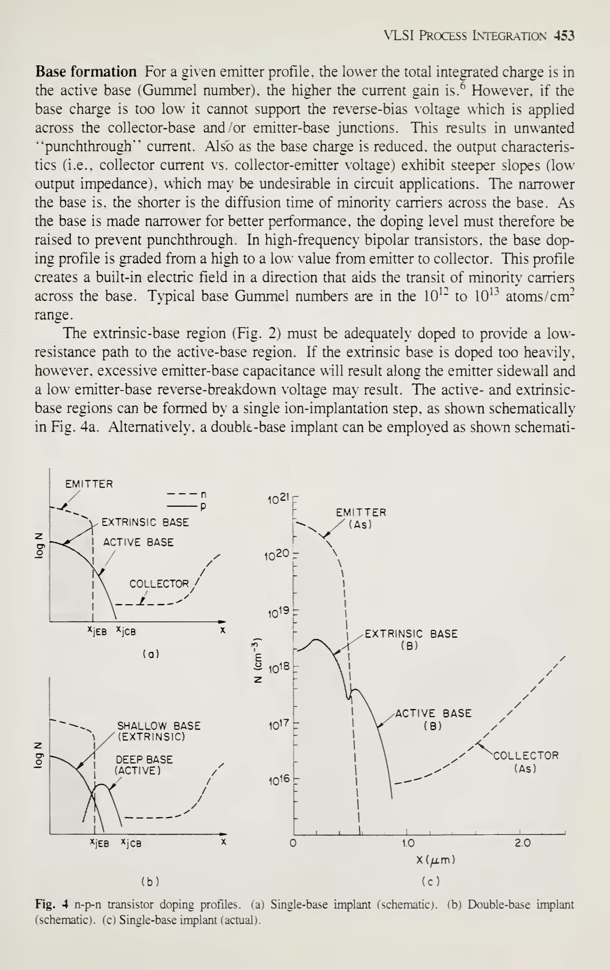
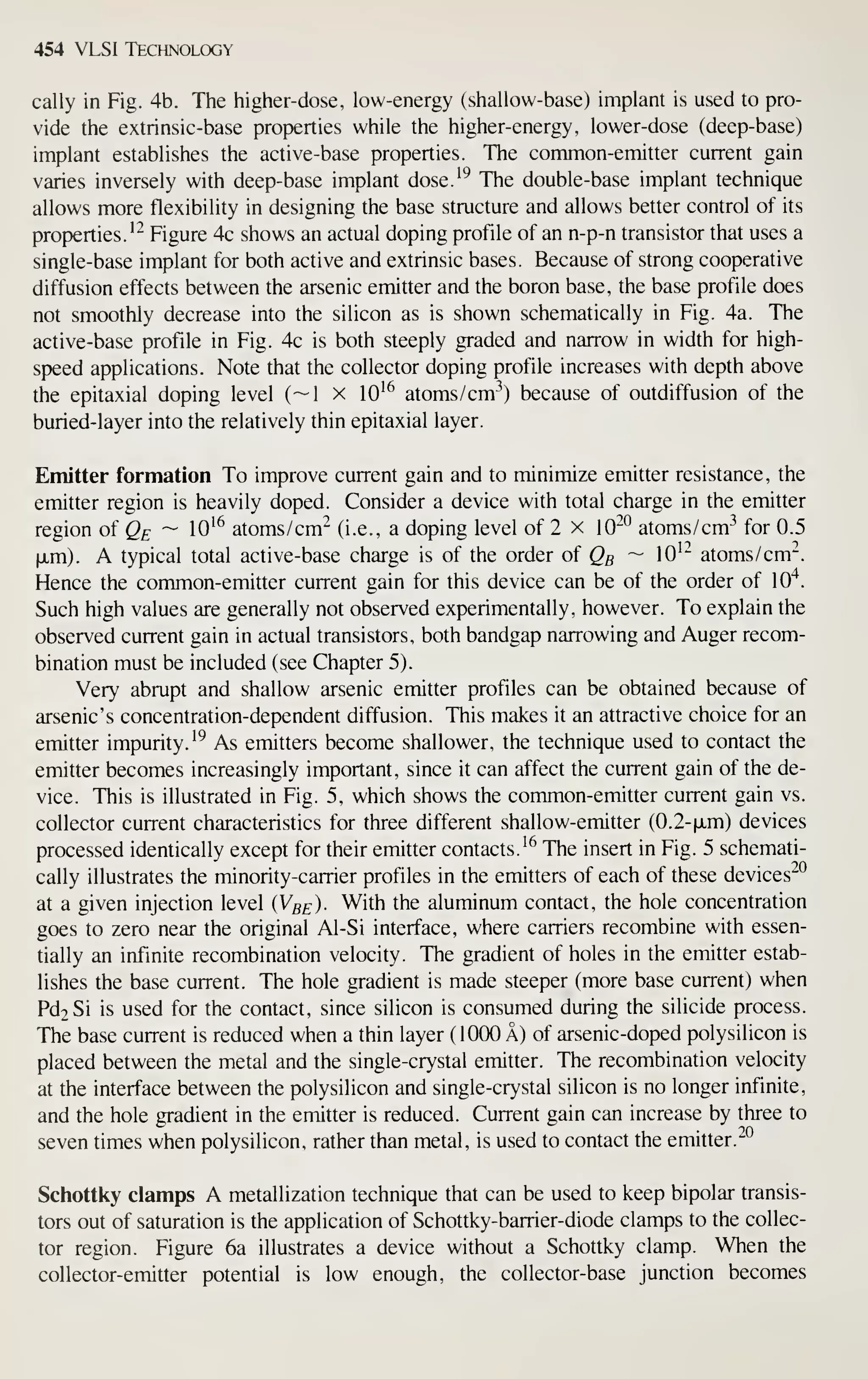
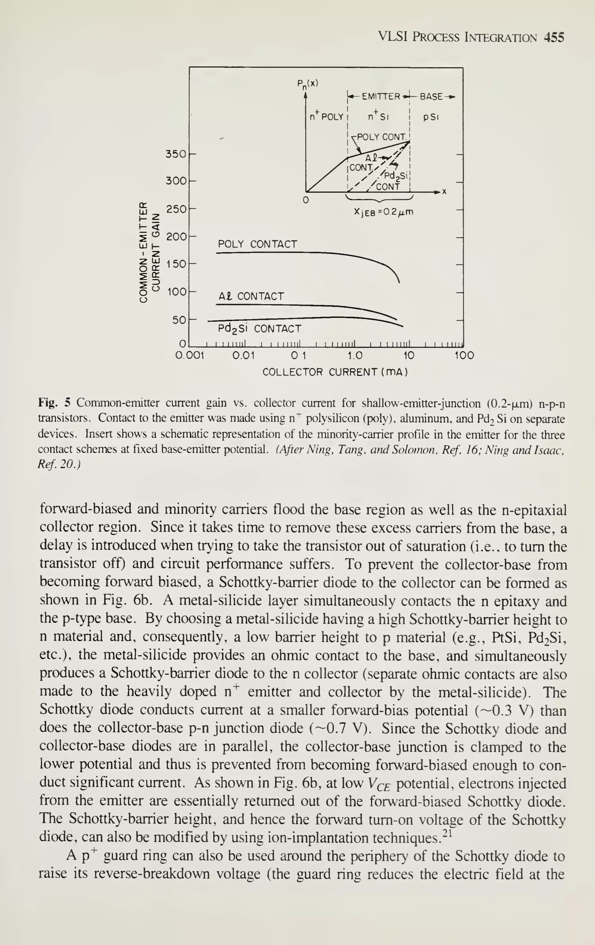
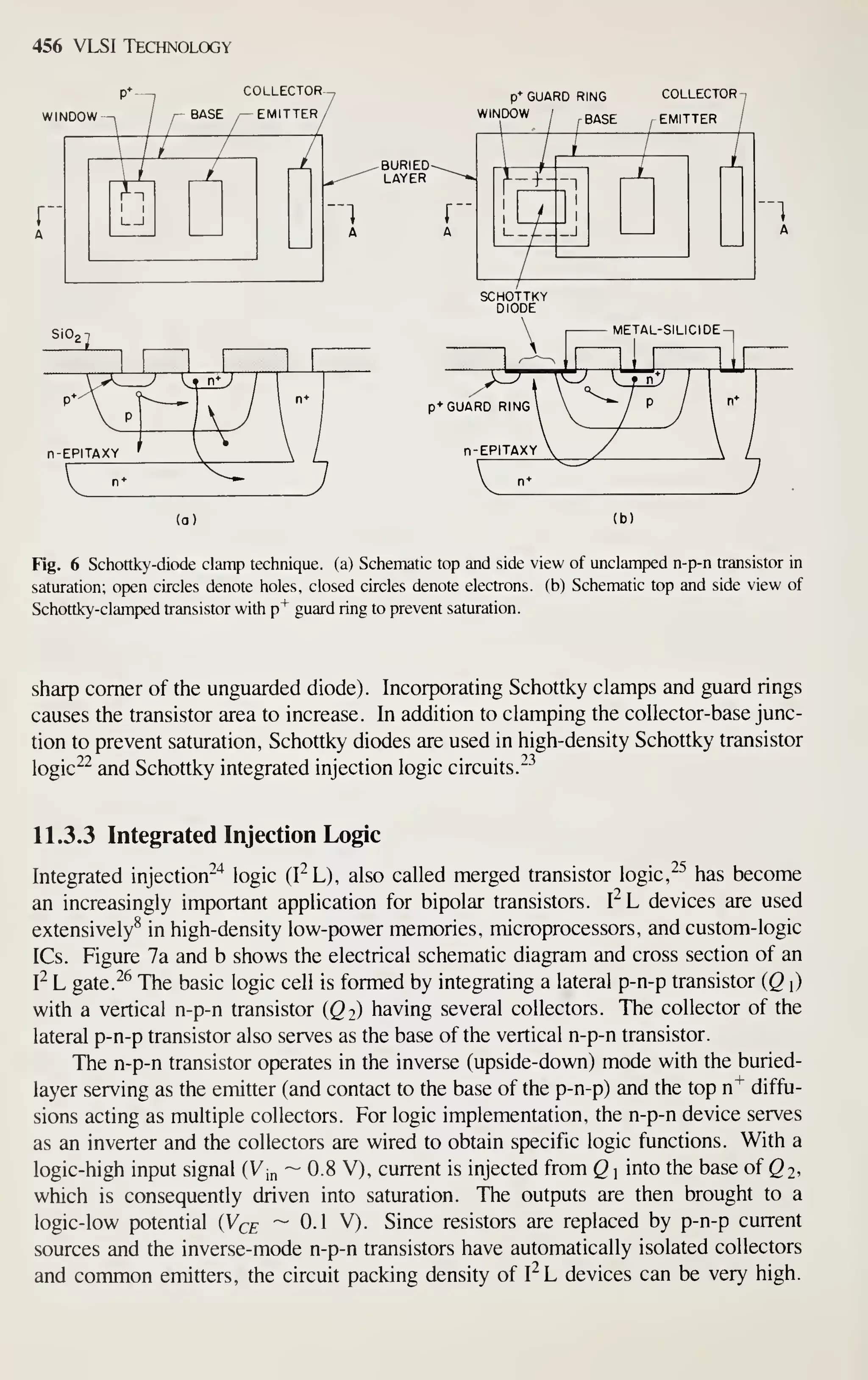
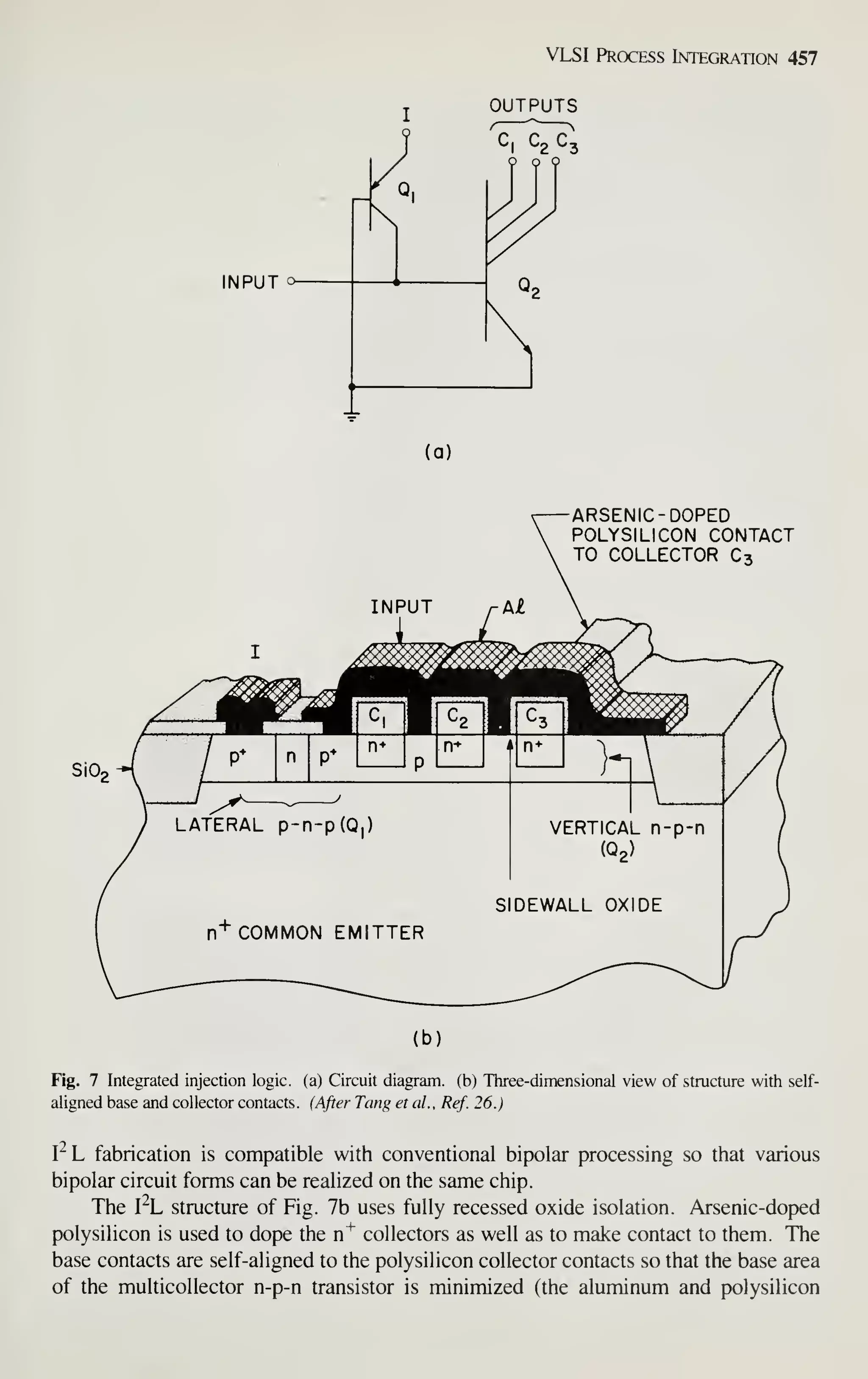
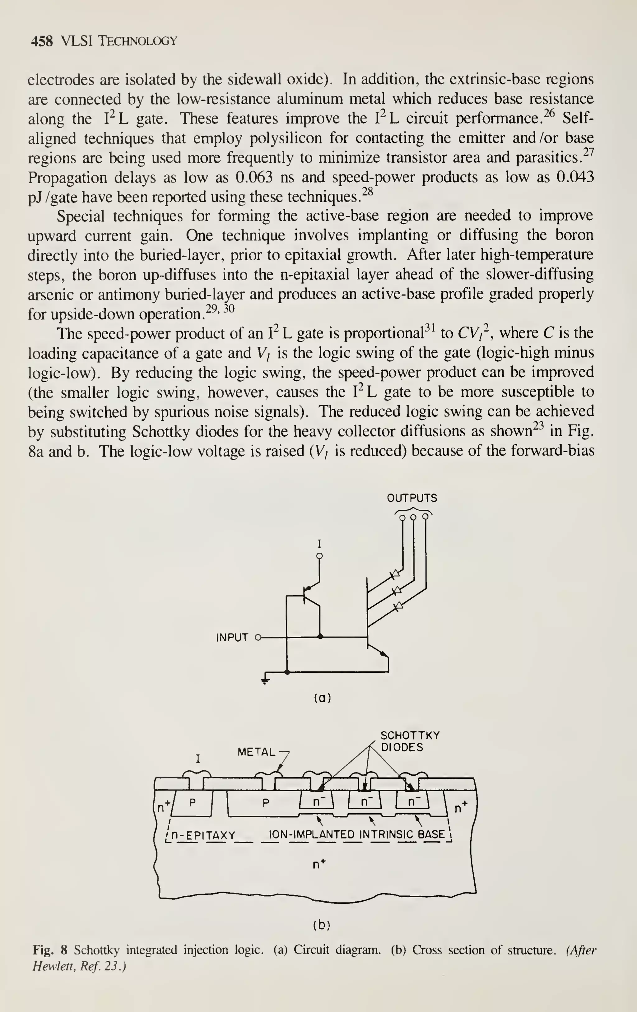
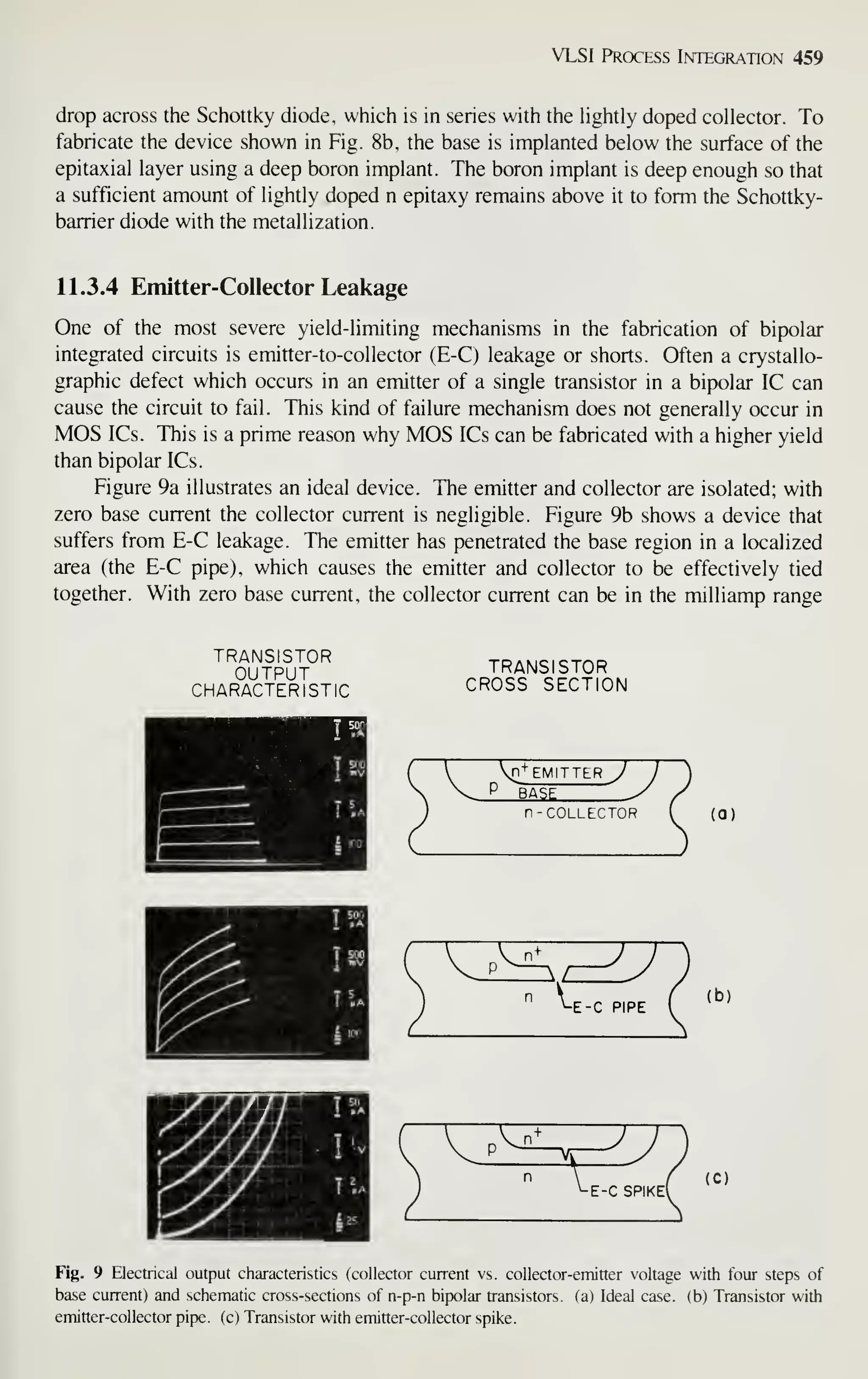
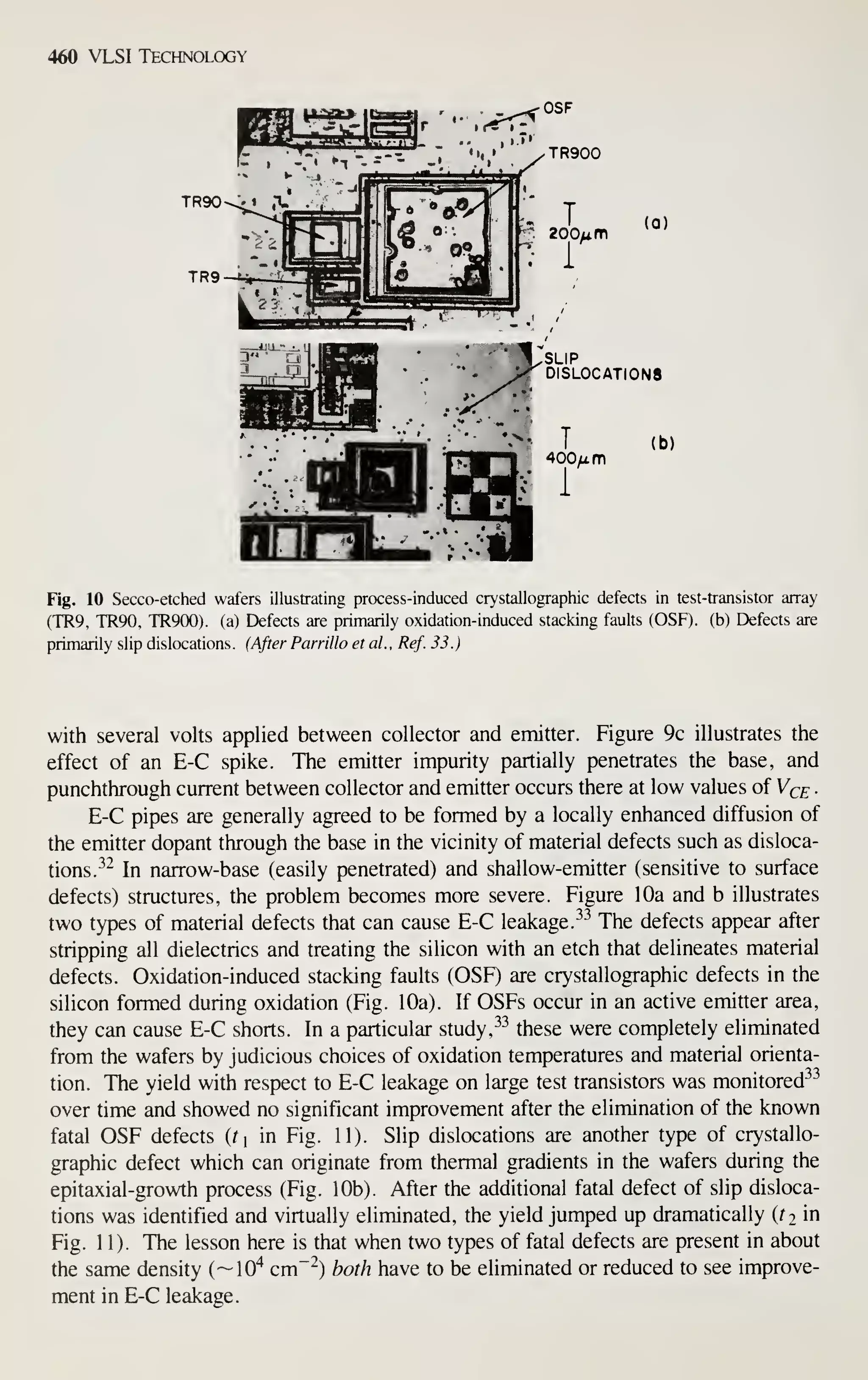
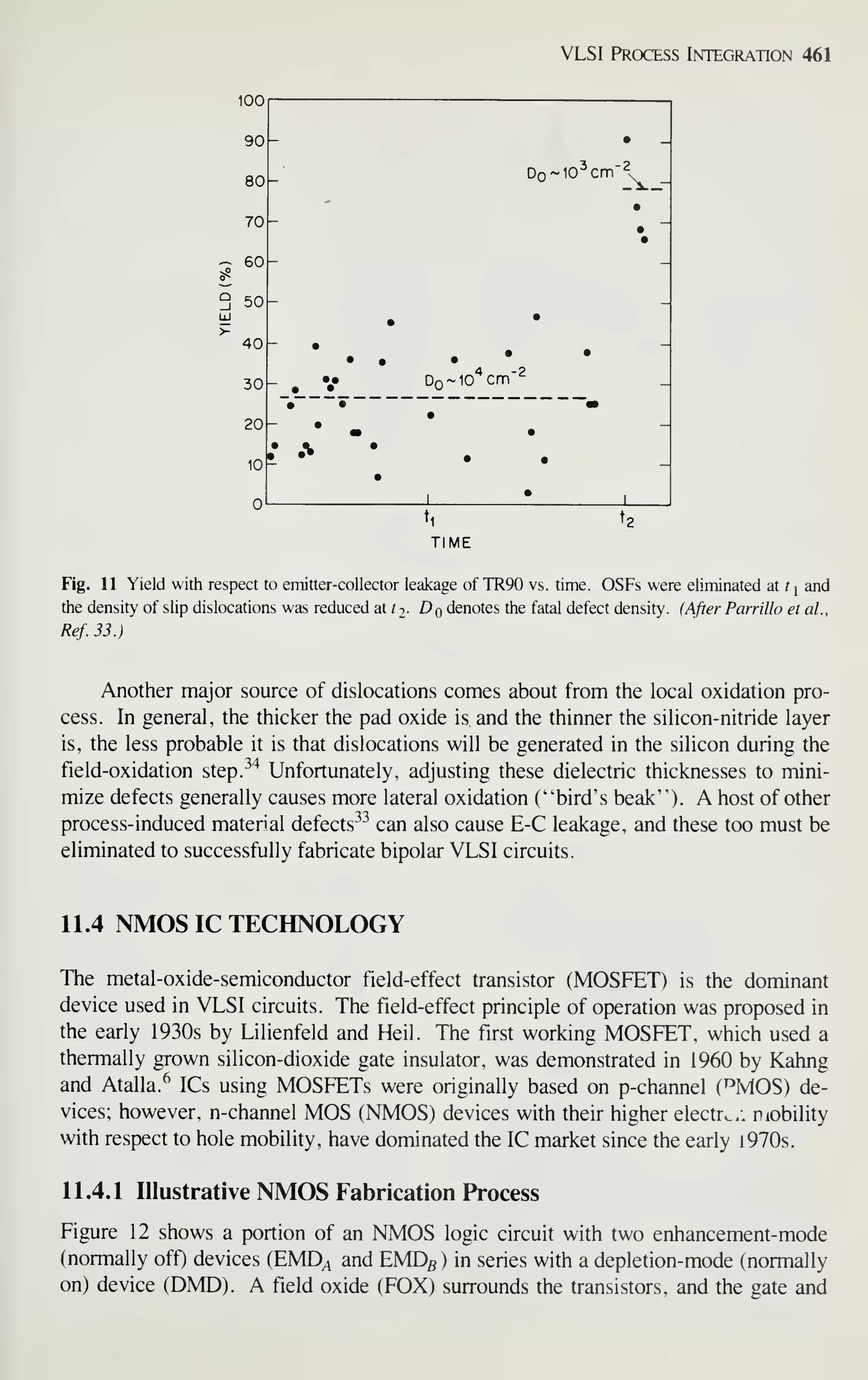
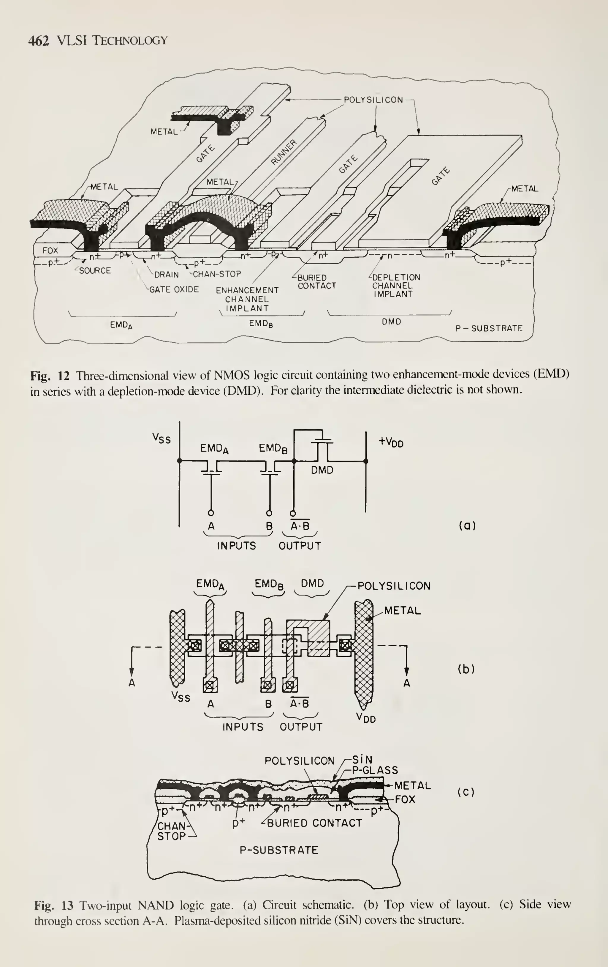
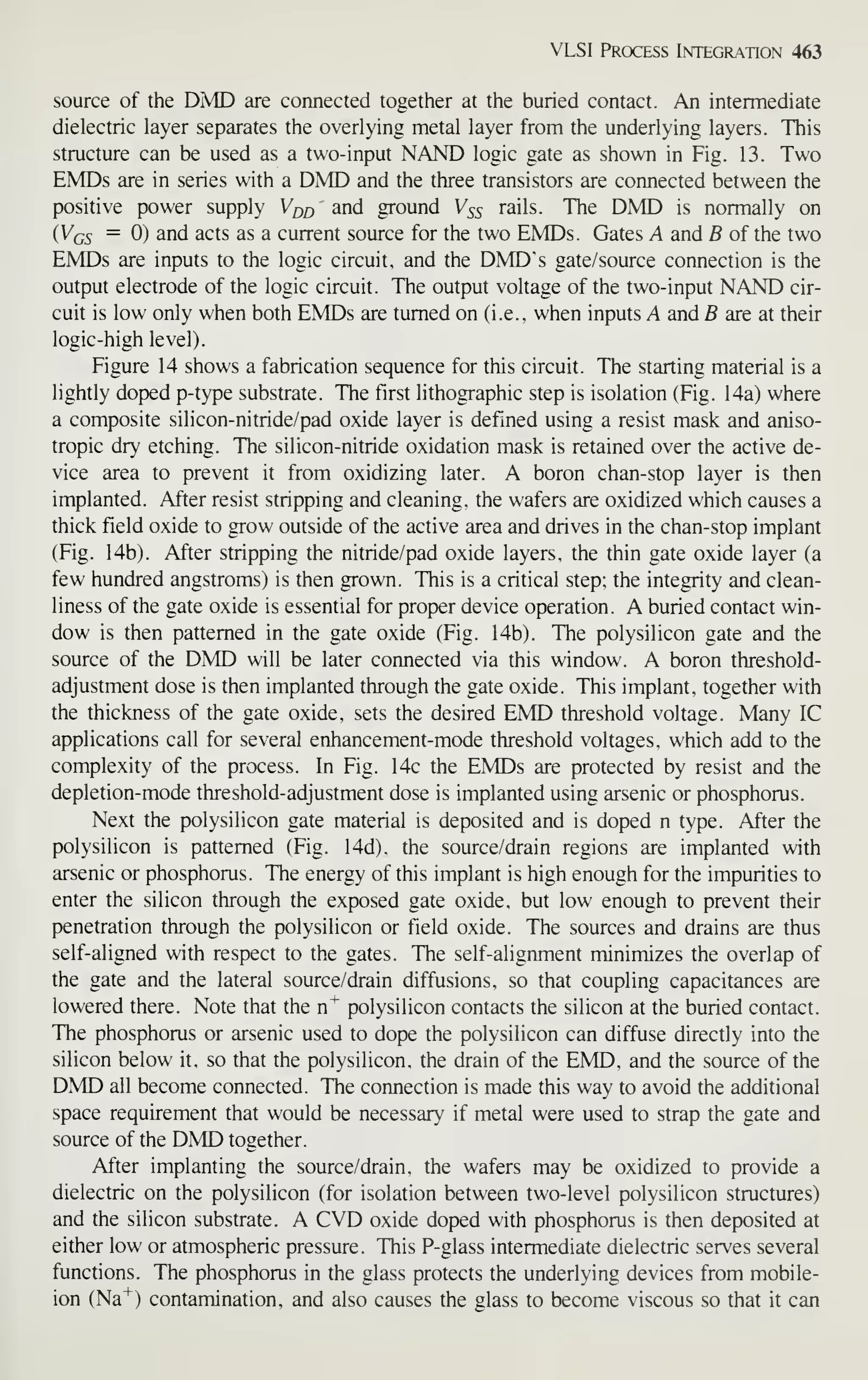
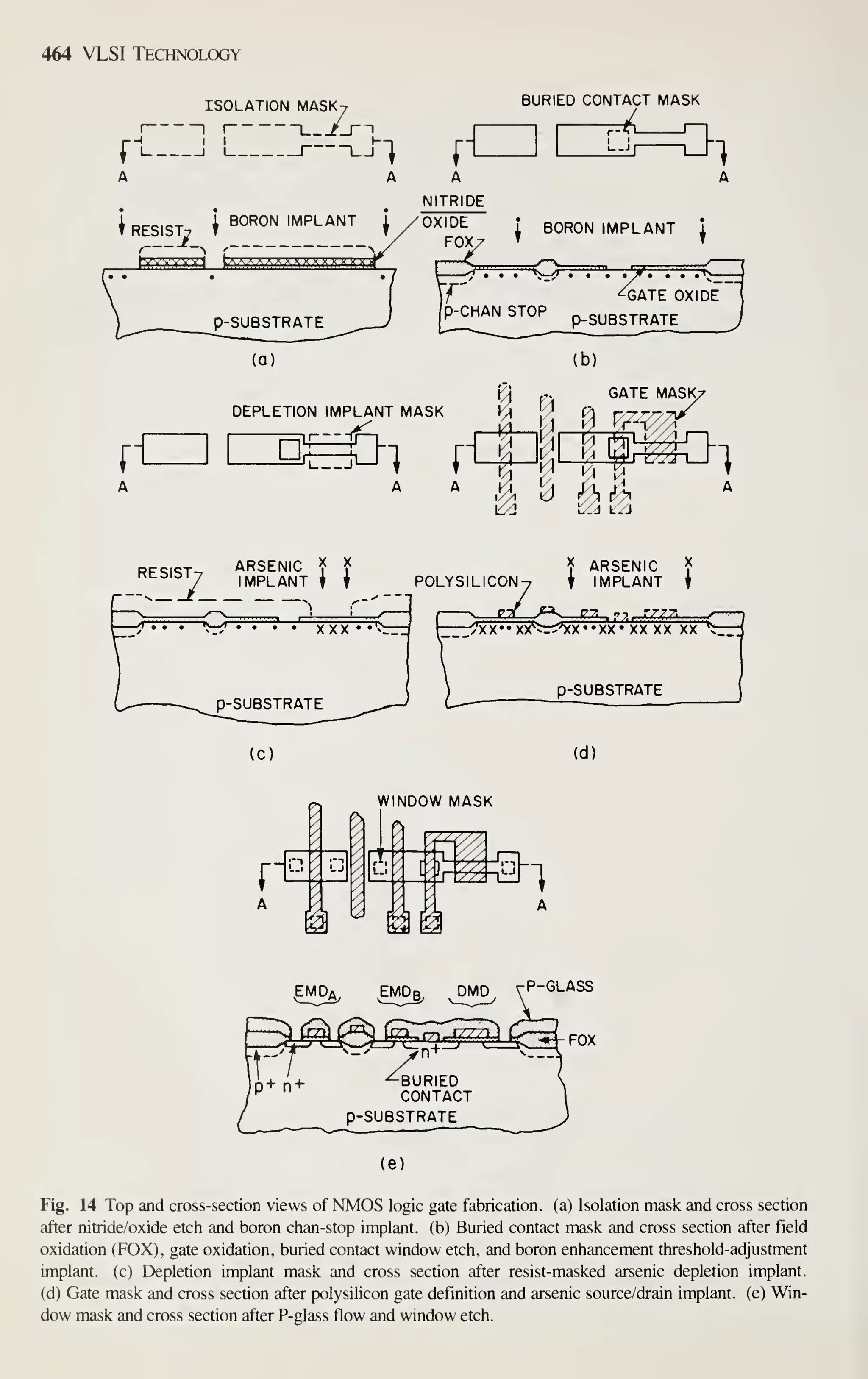
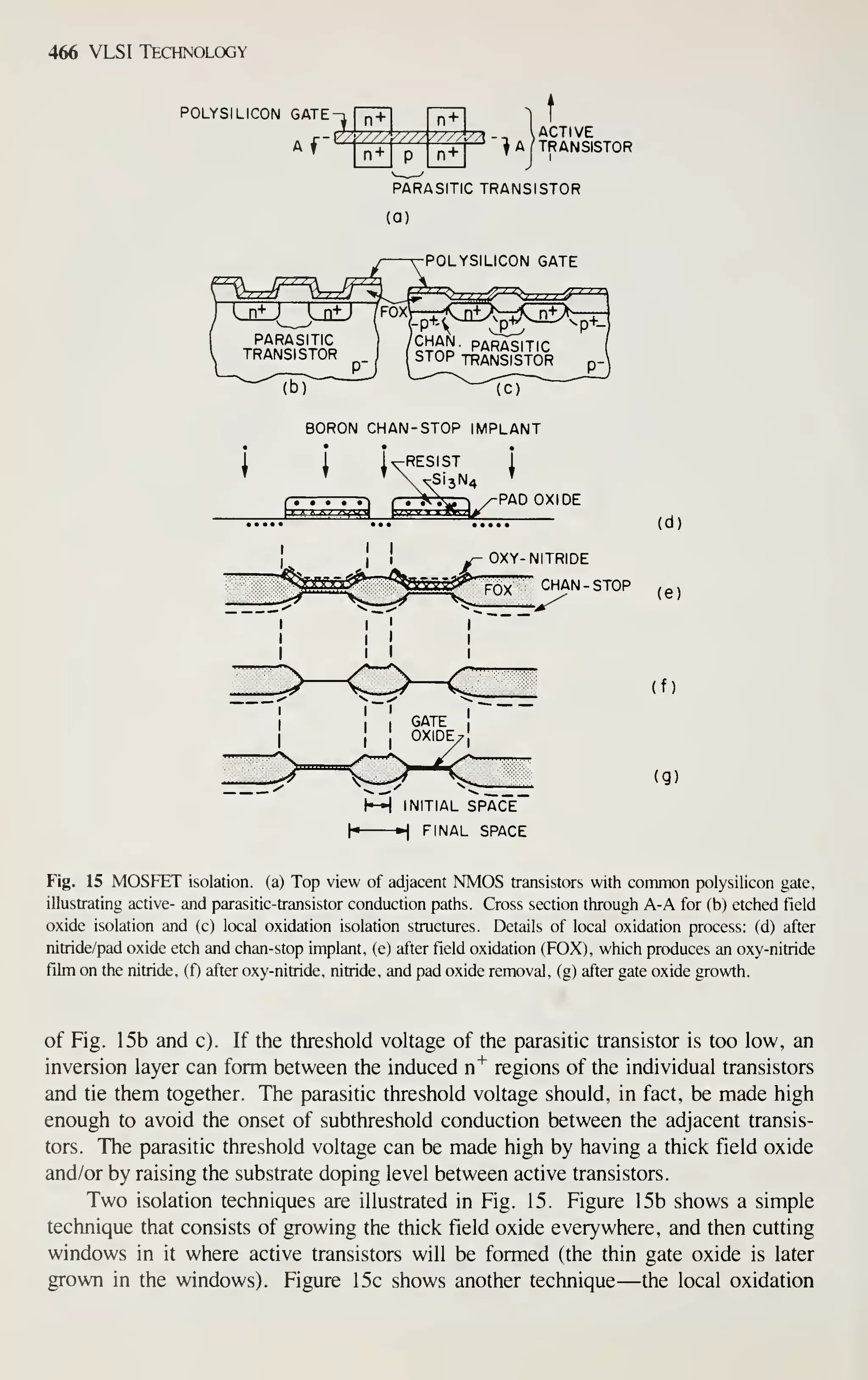
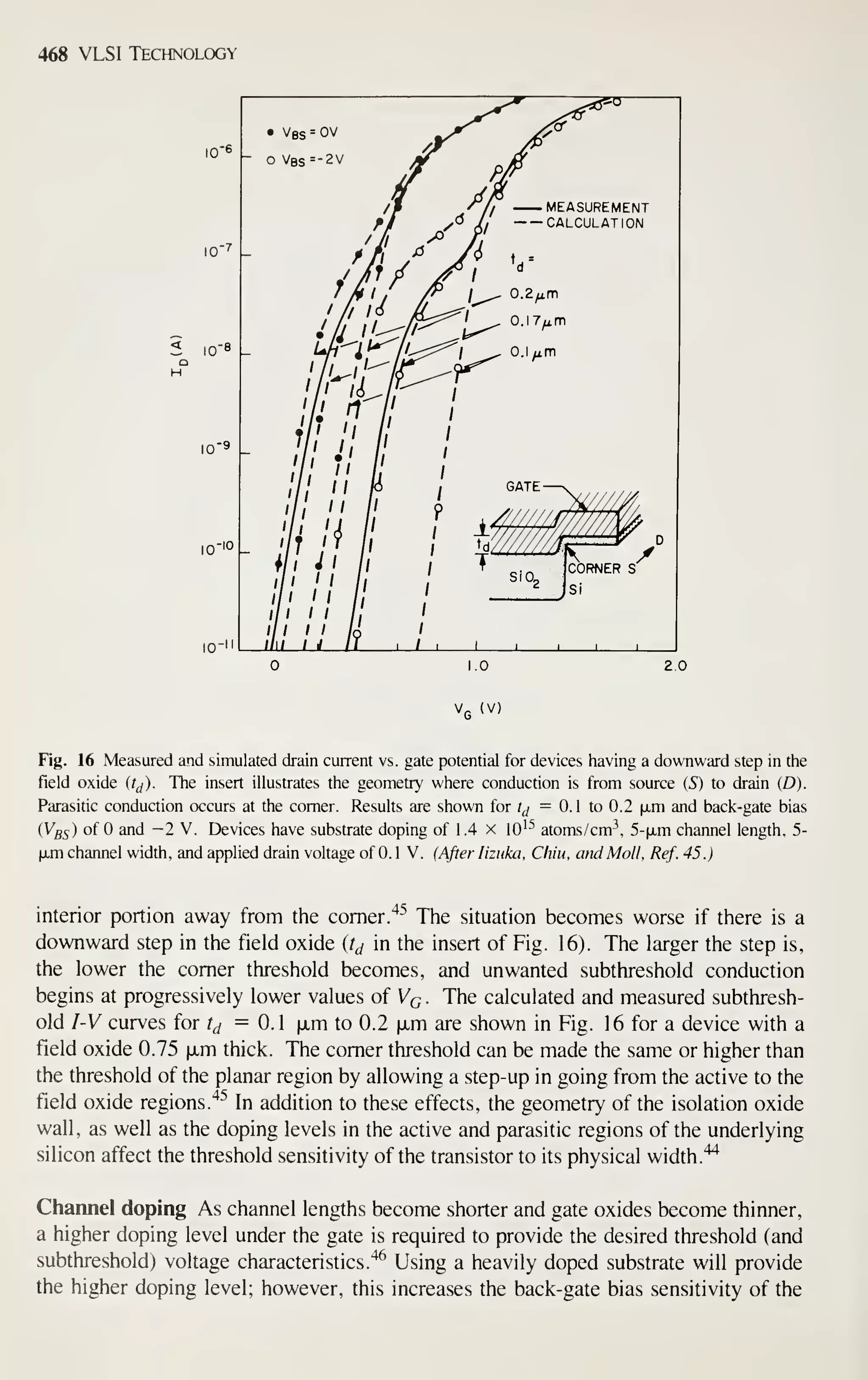
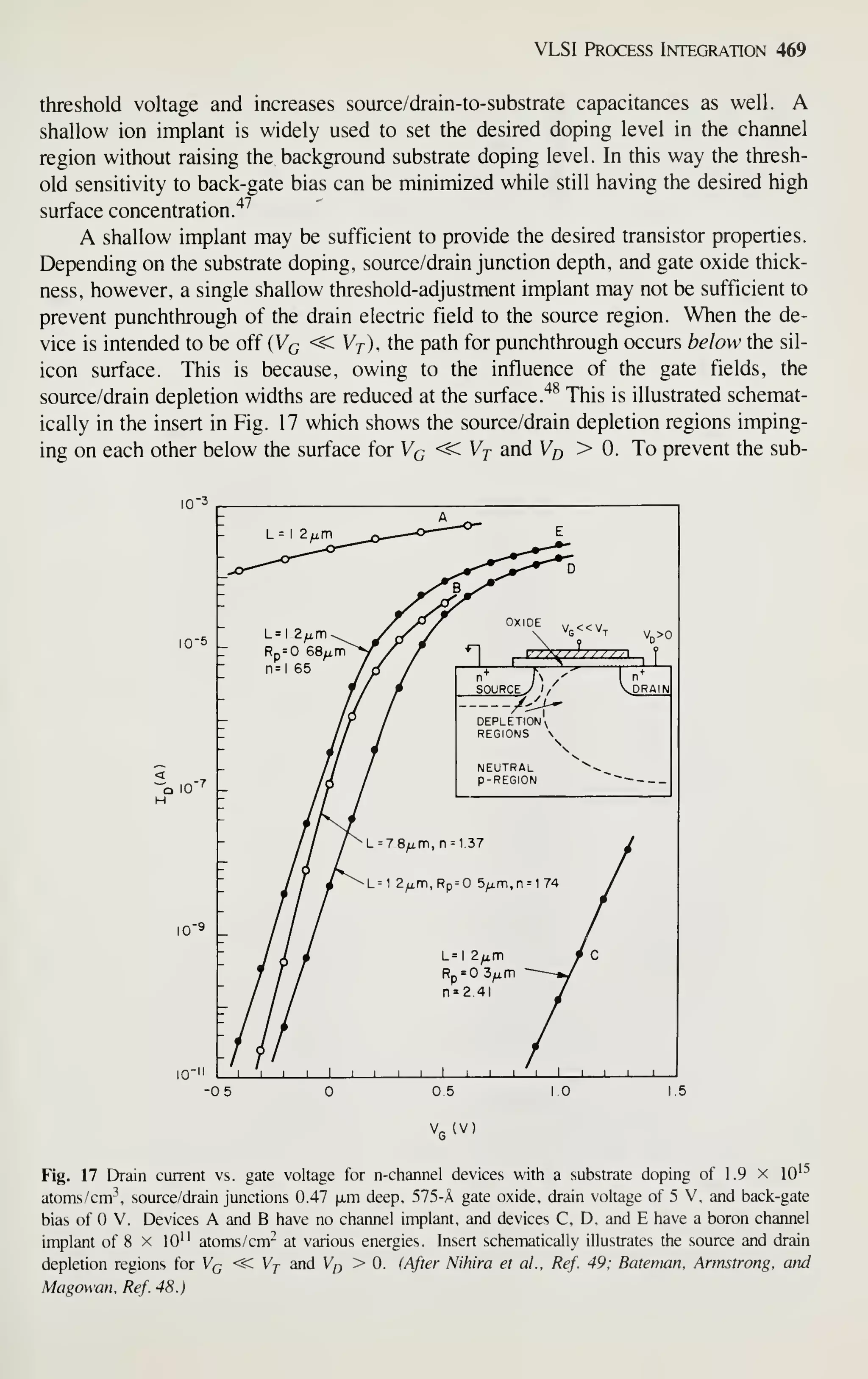
![470 VLSI Technology
surface punchthrough, a deep boron implant can be used to raise the substrate doping
level at the appropriate depth. Figure 17 illustrates subthreshold I-V curves for a de-
vice with a light substrate doping."^^ A short-channel device (L =1.2 |jLm) punches
through badly (curve A). Curve B shows the desired behavior of a long-channel
(L =7.8 fxm) transistor in the same substrate. A boron implant dose of 8 x lO''
atoms/cm^ was implanted in the short-channel device at a projected range of 0.3 |JLm.
This was too shallow, and the threshold voltage (curve C) rose well above the desired
value. By increasing the implant energy (curves D to E), the deep boron implant
became deep enough to allow the desired low threshold voltage (surface concentration
undisturbed) and to prevent punchthrough (peak of implant at 0.68 fxm below the sur-
face) in the 1.2-fjLm-long device. Of course the back-gate bias sensitivity increases
also. Note that the subthreshold swing factor [n = q lkT{dVc Id log /^ )] is large
{n =2.41) for the shallow implant (curve C) and becomes smaller (n = 1 .65) as the
implant is made deeper. This occurs because the high-doping region is pushed below
the silicon surface. Two boron implants can be used to establish the surface doping
for the desired threshold voltages of short-channel devices (shallow implant) and to
tailor the subsurface profile to prevent punchthrough (deep implant). ^'^^ ^'
A deleterious consequence of increasing the surface concentration is the accom-
panying reduction in carrier mobility at the surface. This reduction in surface mobil-
ity is caused by the increased vertical electric field experienced by the carriers in the
channel—which in turn is a consequence of the more heavily doped substrate.
^^'^^
Using ion implantation to form a shallow p-n junction at the surface, and choosing a
gate material with an appropriate work function, can increase the electron^"^ and
hole^^ mobilities above the mobilities found in conventional structures.
The discussion, so far, has centered around surface-channel conduction. Buried-
channel devices, however, are becoming increasingly common in ICs. They are gen-
erally of two types —normally on and normally off. An example of a normally on
buried n-channel was discussed in connection with Fig. 13, where an arsenic surface
layer provides the source-to-drain conduction at zero gate voltage. A normally off
buried n-channel device can be fabricated in a similar manner (n-type surface layer in
a p-type substrate). However, a gate material with a suitably large work-function is
chosen (e.g.,
p"*"
polysilicon^^ or MoSi2^^) to deplete the n-type surface layer of car-
riers, and to produce the normally off characteristics. When the device is turned on,
much of the current is conducted below the surface (where bulk mobility is larger than
surface mobility); thus the buried-channel device has significantly higher carrier
mobility than conventional devices. However, since the conduction path is further
removed from the gate than in conventional surface-channel devices, the transconduc-
tance gy^ = (dlfj / OVq) y can suffer. These competing effects must be weighed
against each other to ascertain the effect on transconductance.
Gate material Heavily doped n-type polysilicon has been widely used as a gate and
as an interconnect because of its ability to withstand high-temperature processing.
The resistance of the polysilicon (>0 Cl/c) may contribute significantly to the RC
delay of signals that are routed along it. More recently, refractory metals and their
silicides have been used in conjunction with polysilicon^^' ^^ or alone"*'
'^^
to reduce
the resistance. The technique of combining a refractory metal silicide on top of doped](https://image.slidesharecdn.com/simonm-220913174129-44ec6f82/75/Simon-M-Sze-editor-Very-Large-Scale-Integration-VLSI-Technology-McGraw-Hill-Inc-US-1983-pdf-490-2048.jpg)
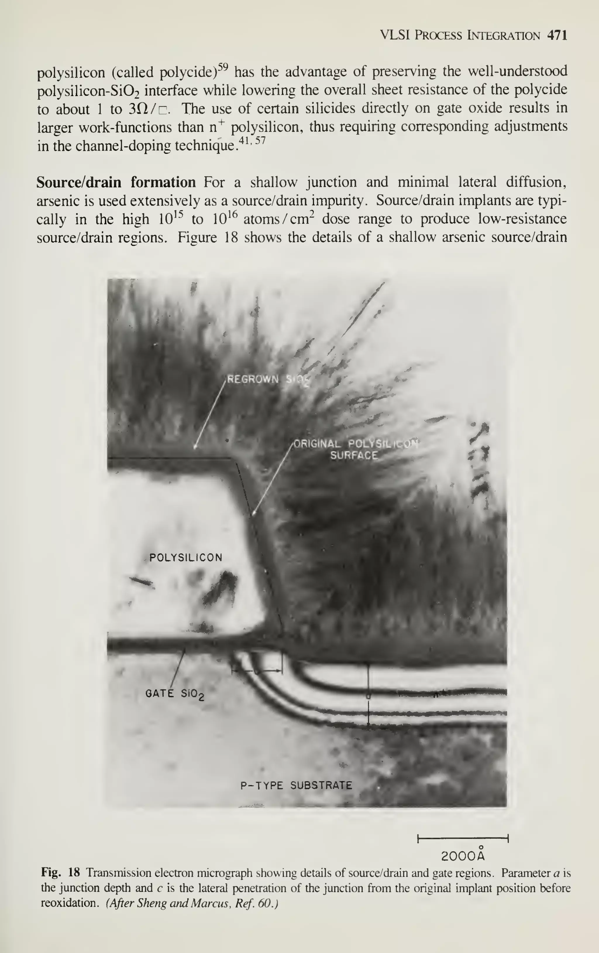
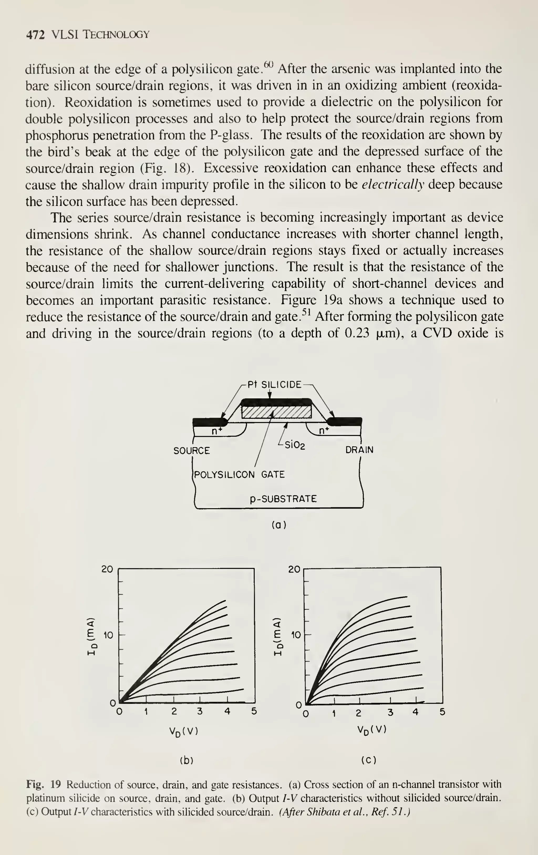
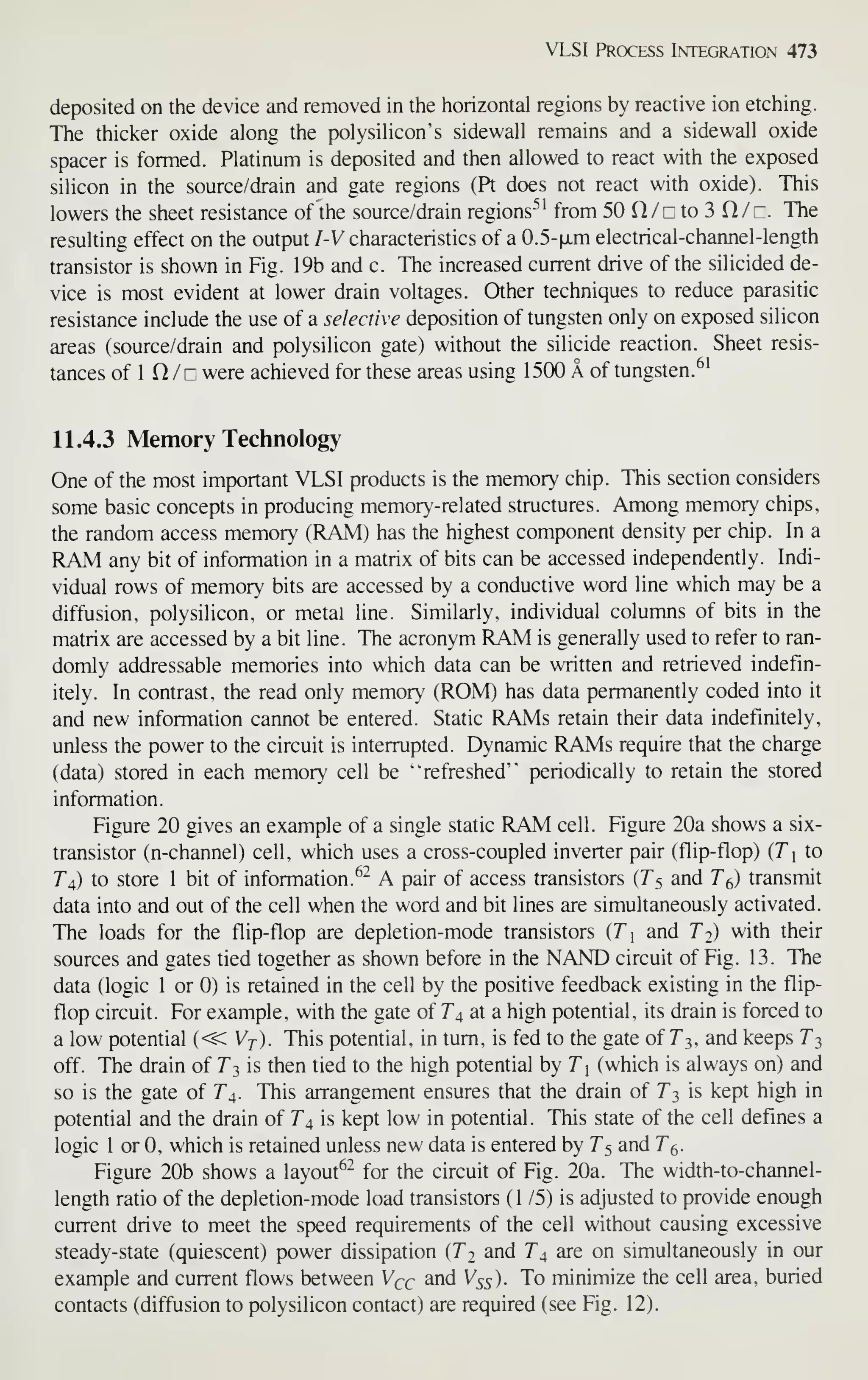
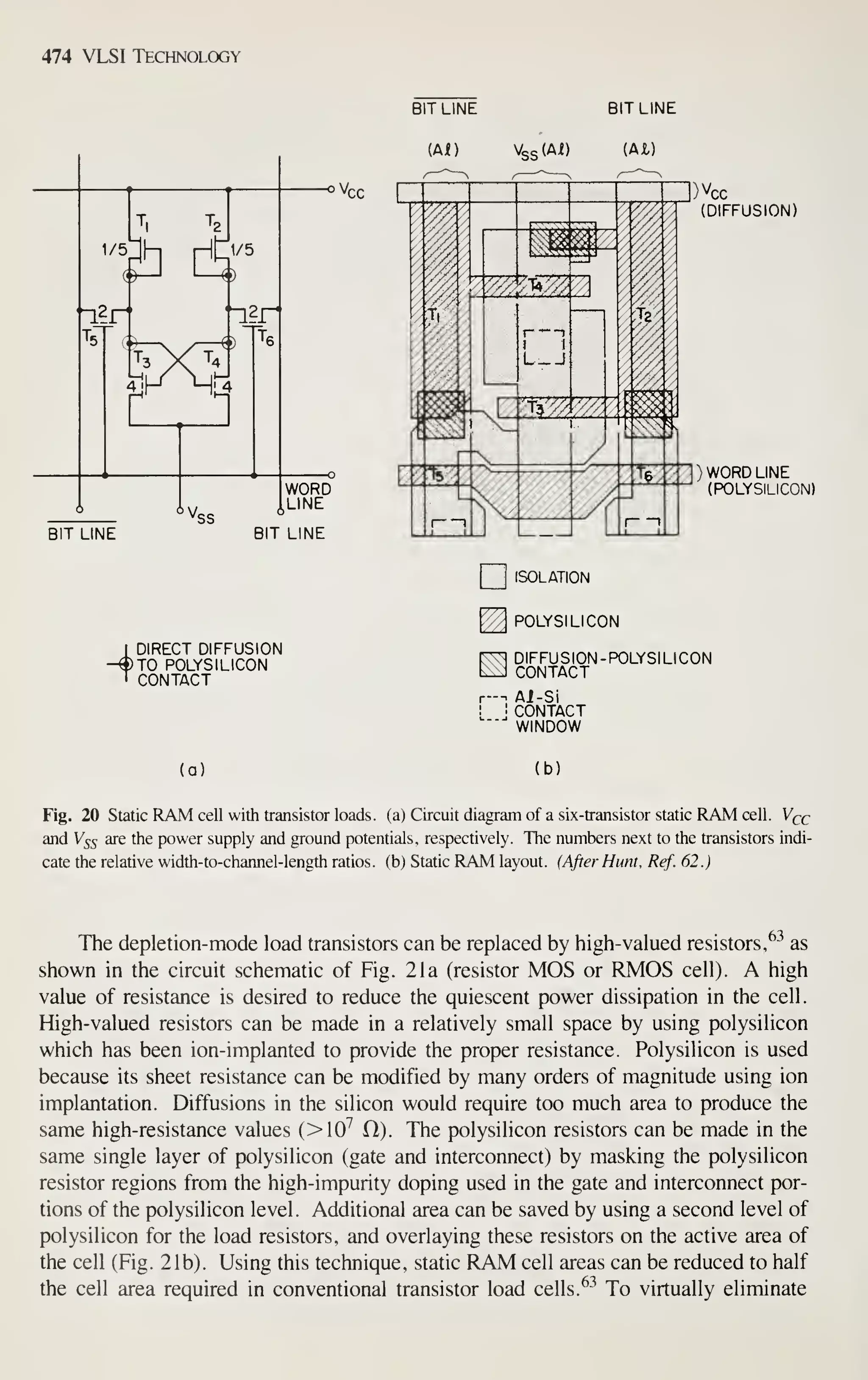
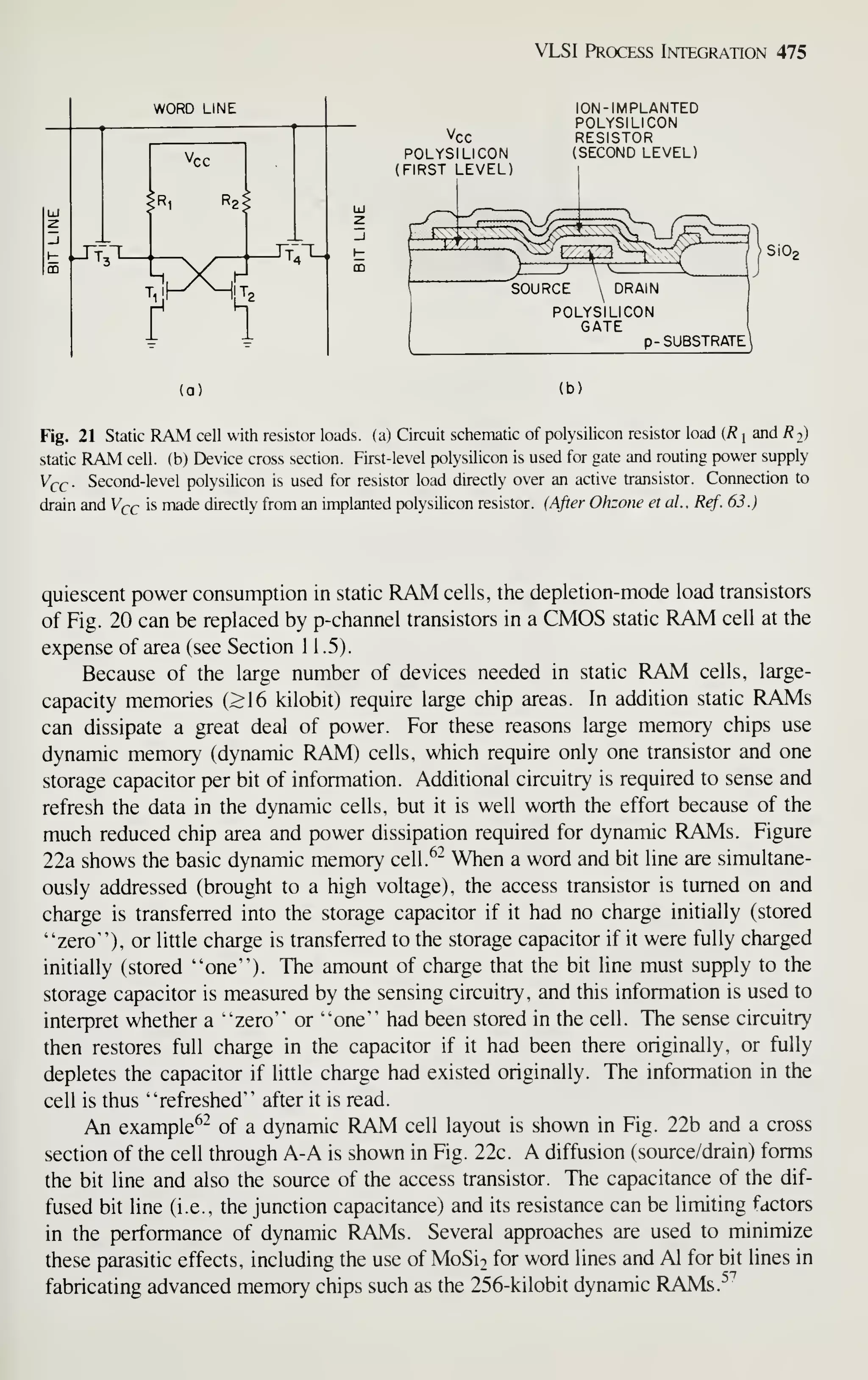
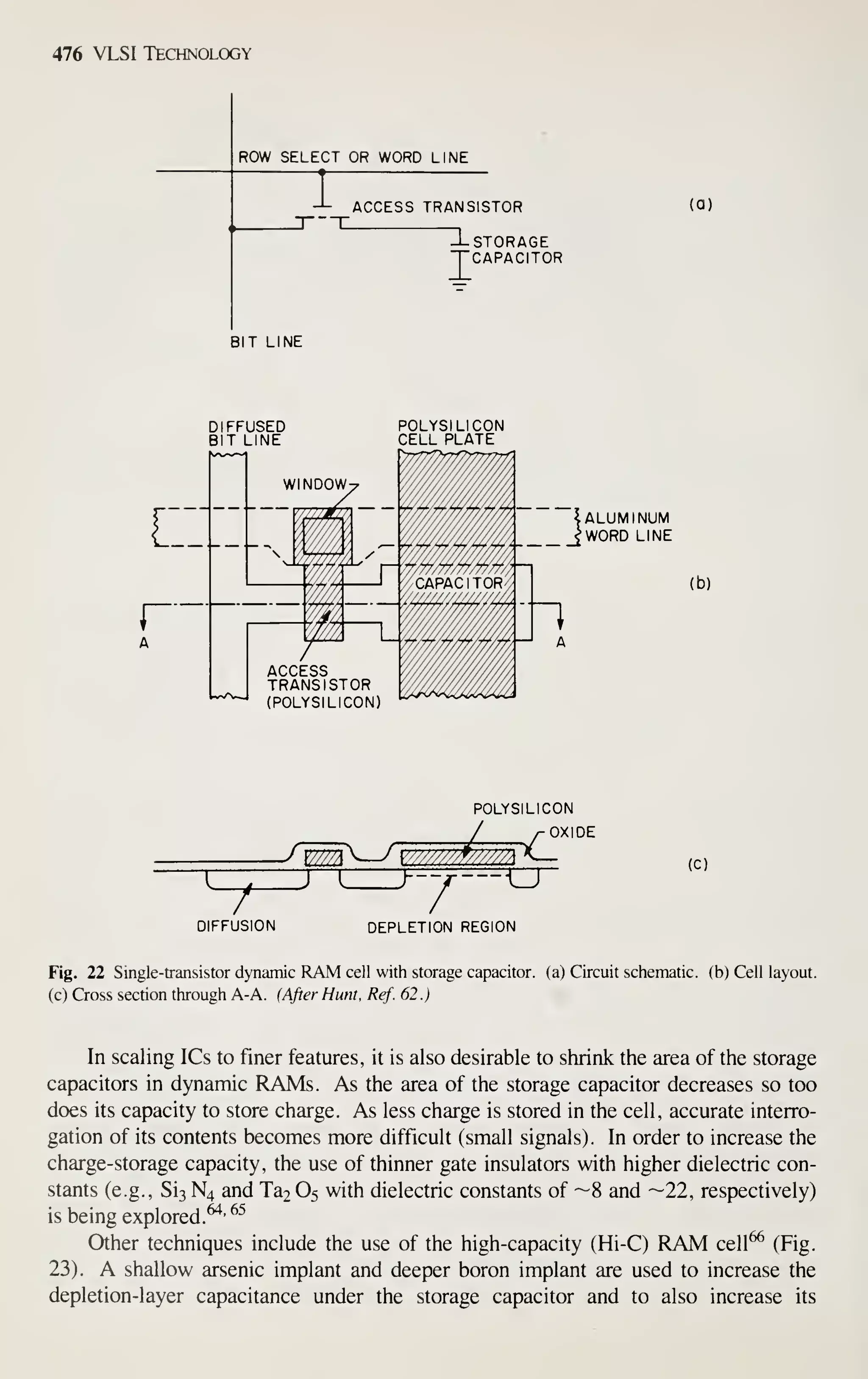
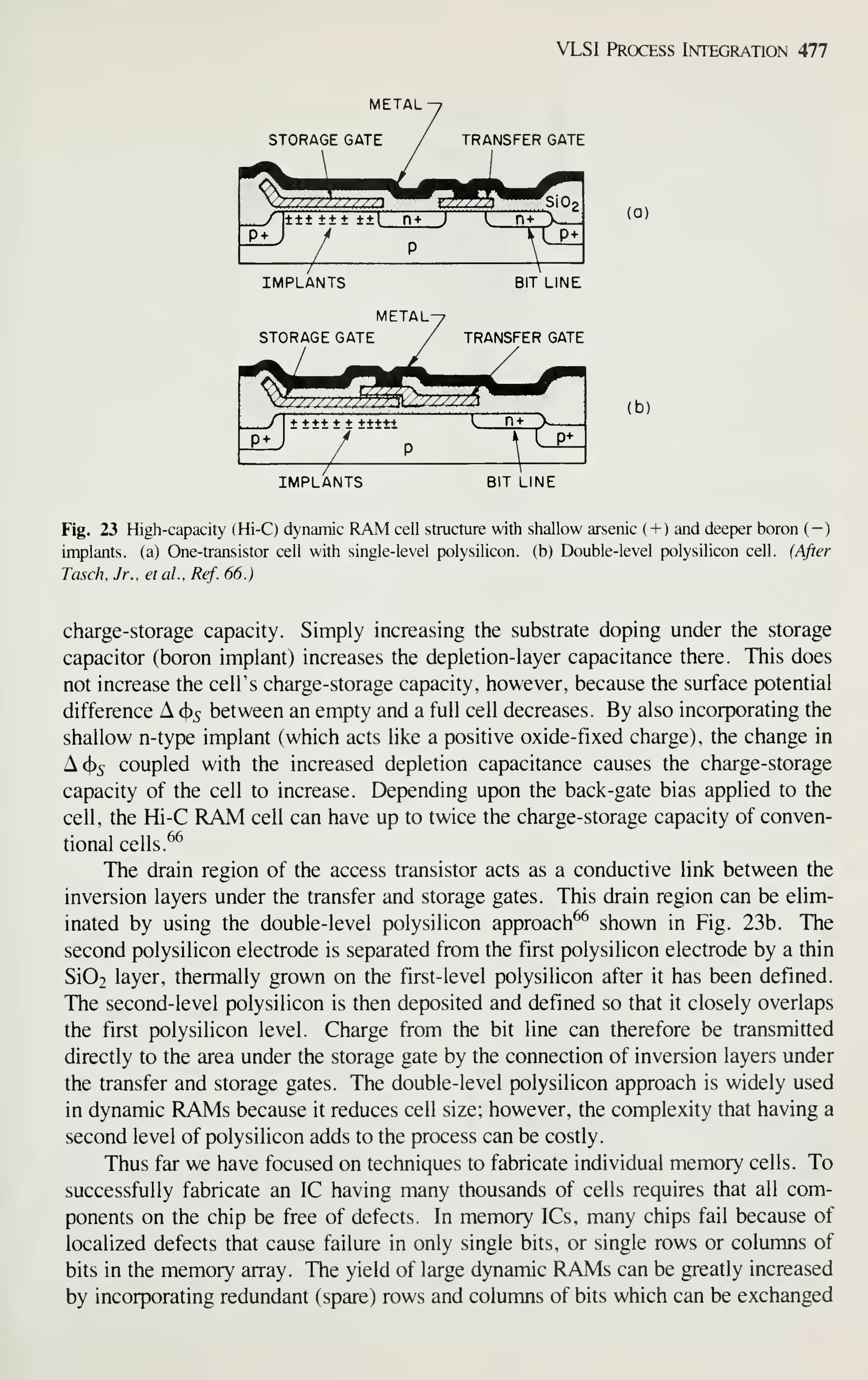
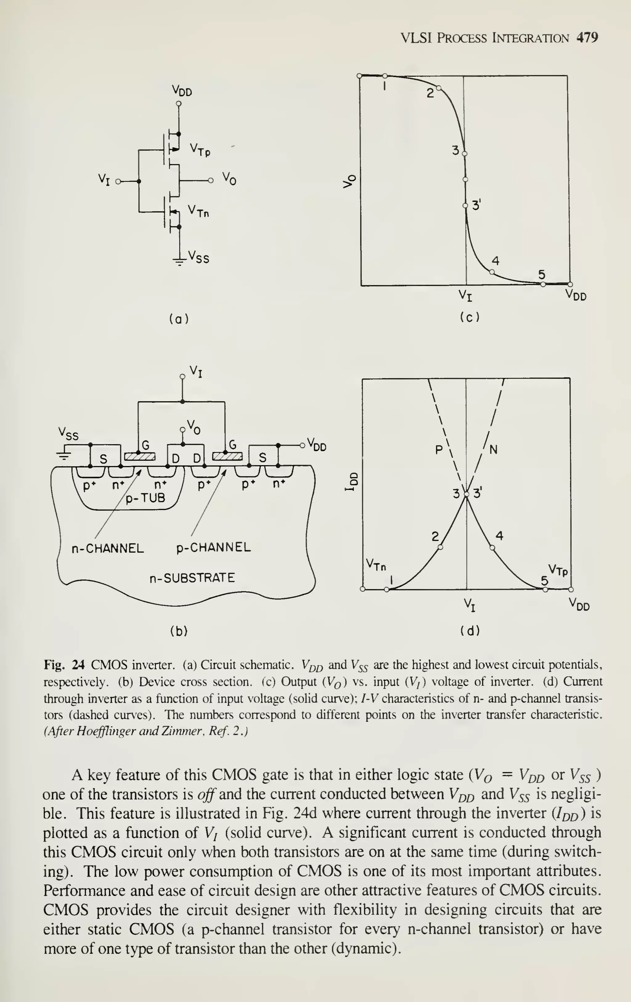
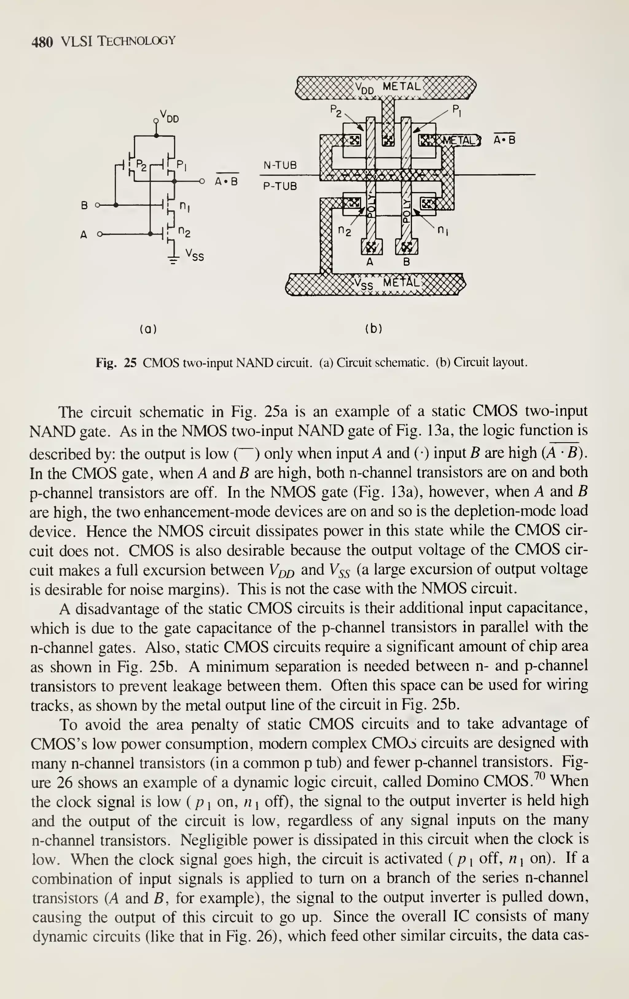
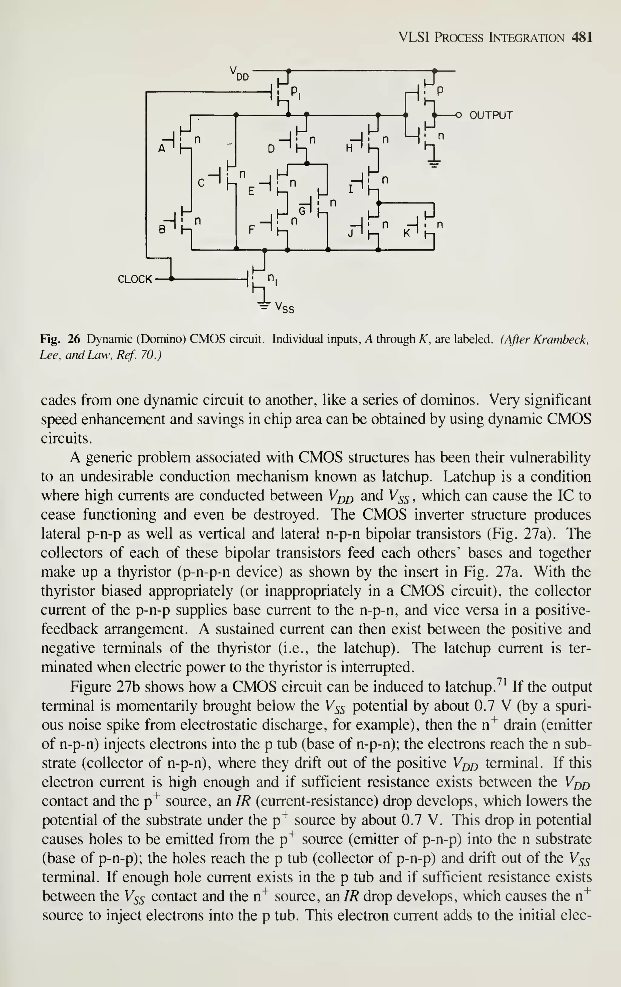
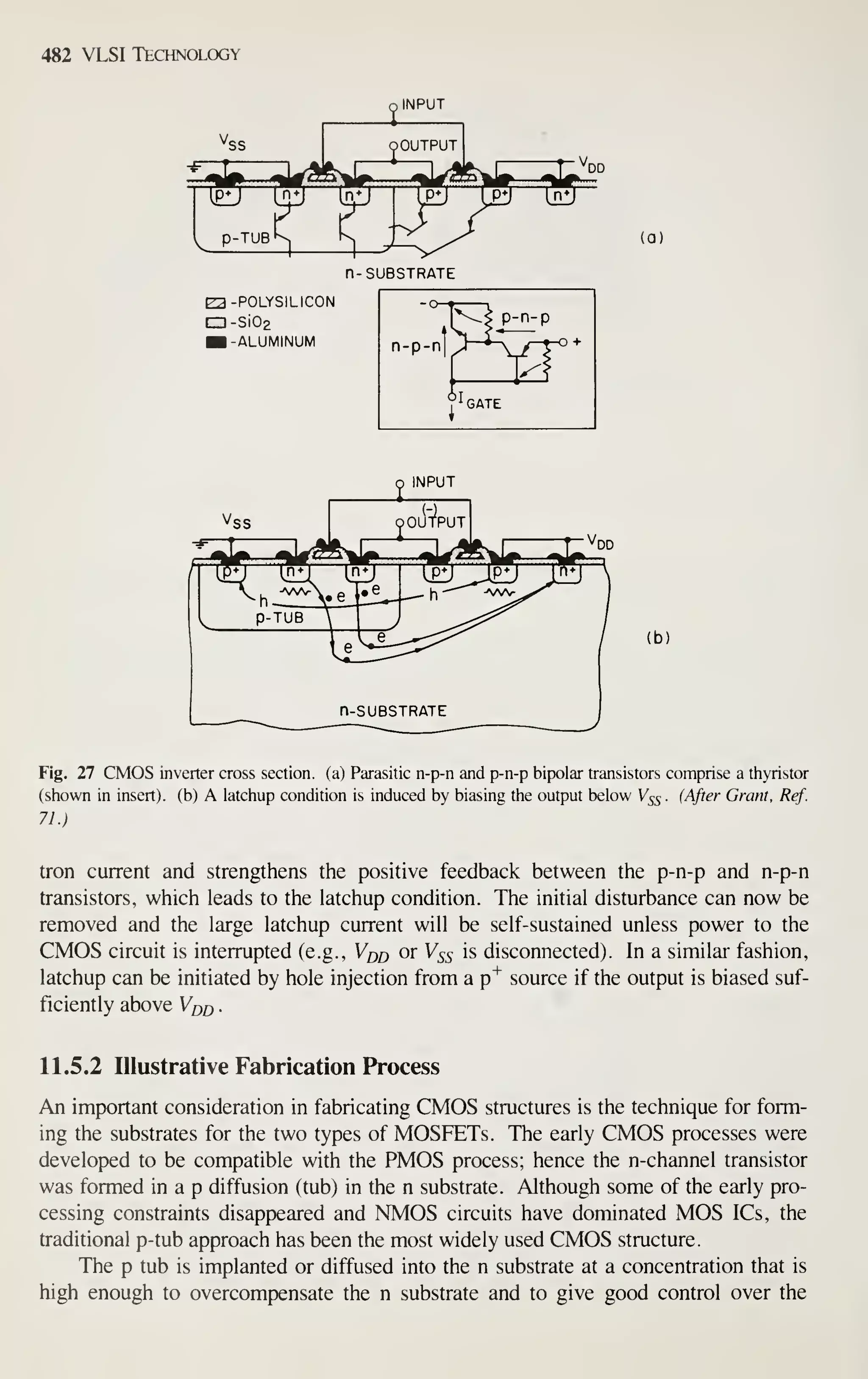
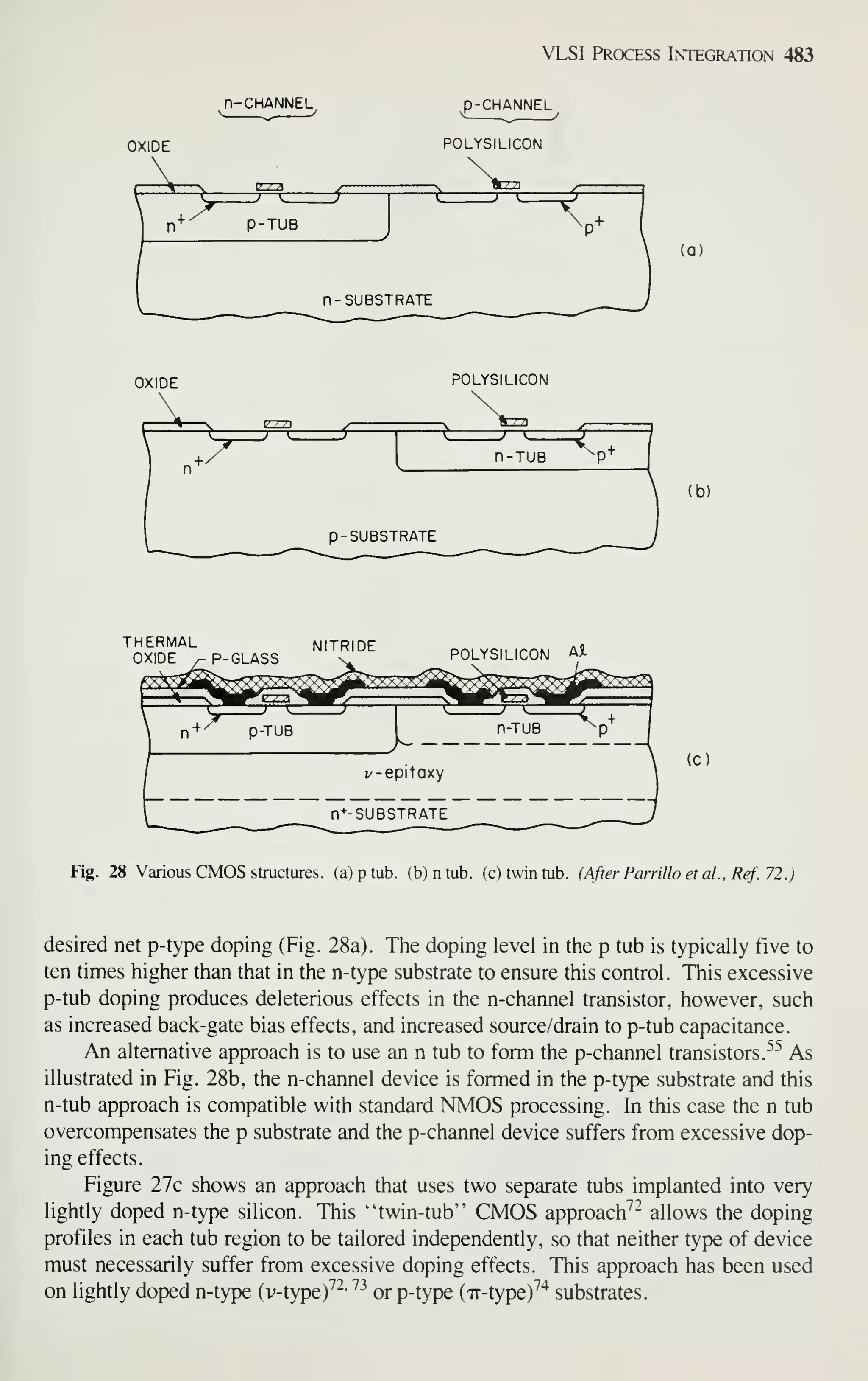
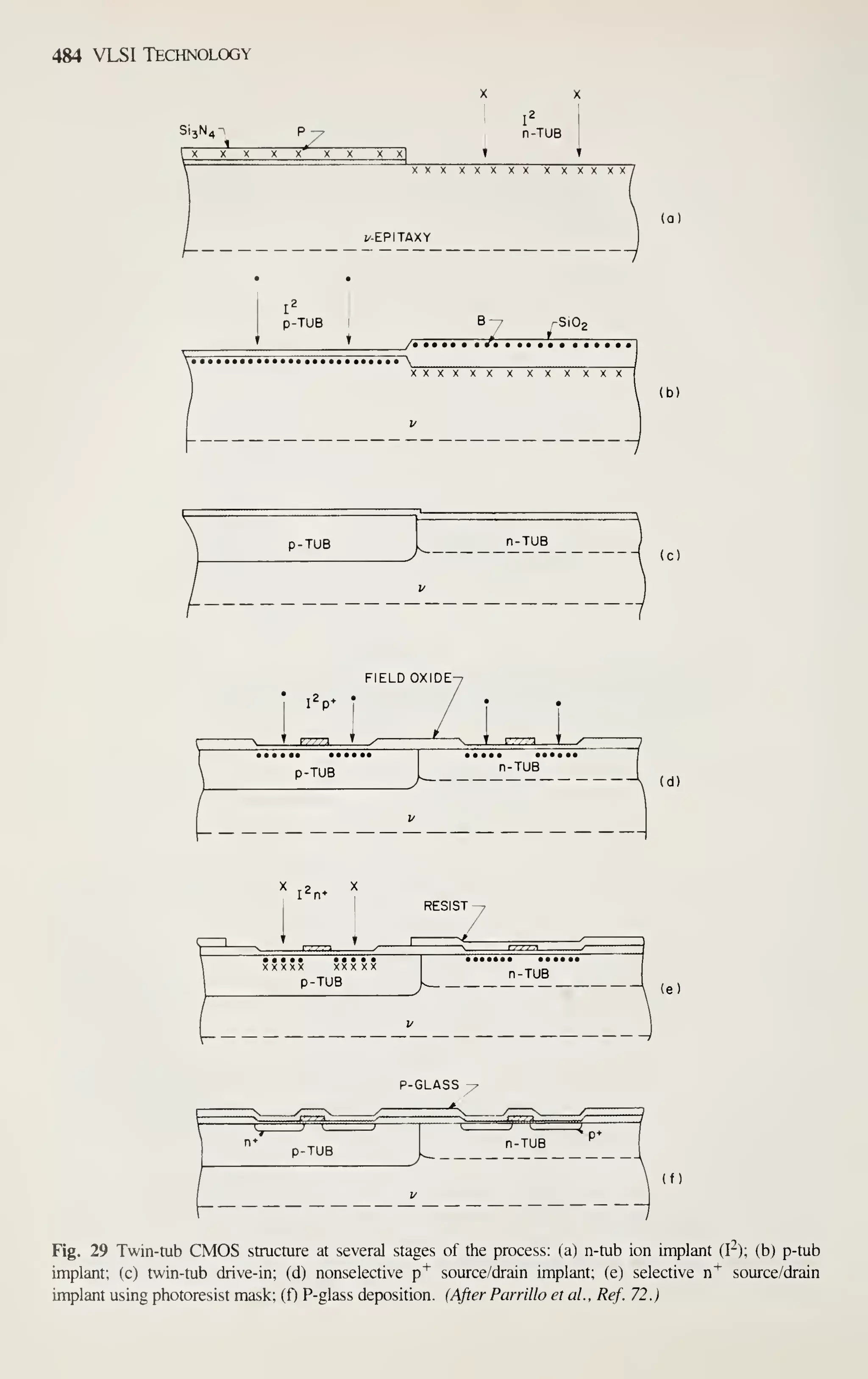
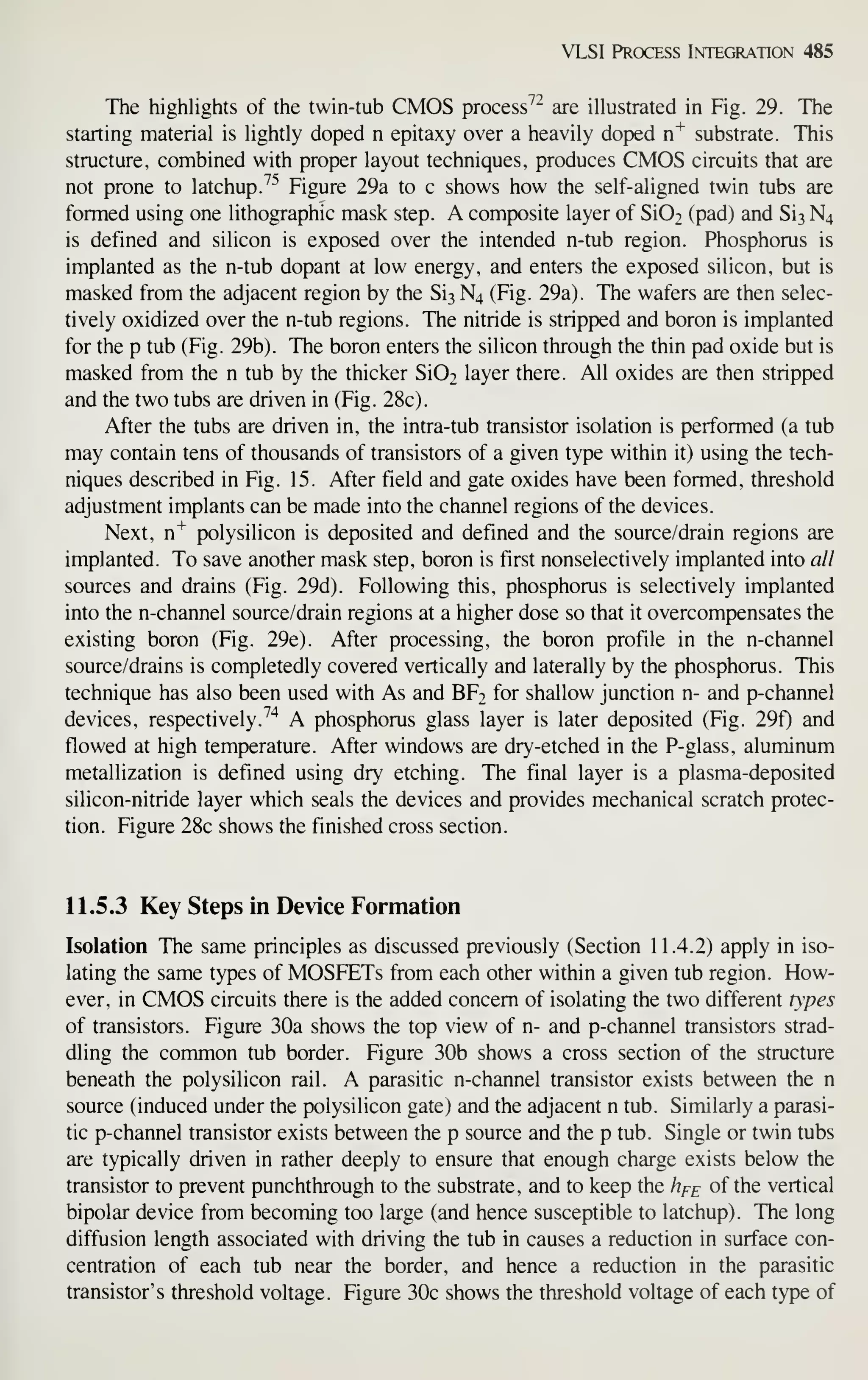
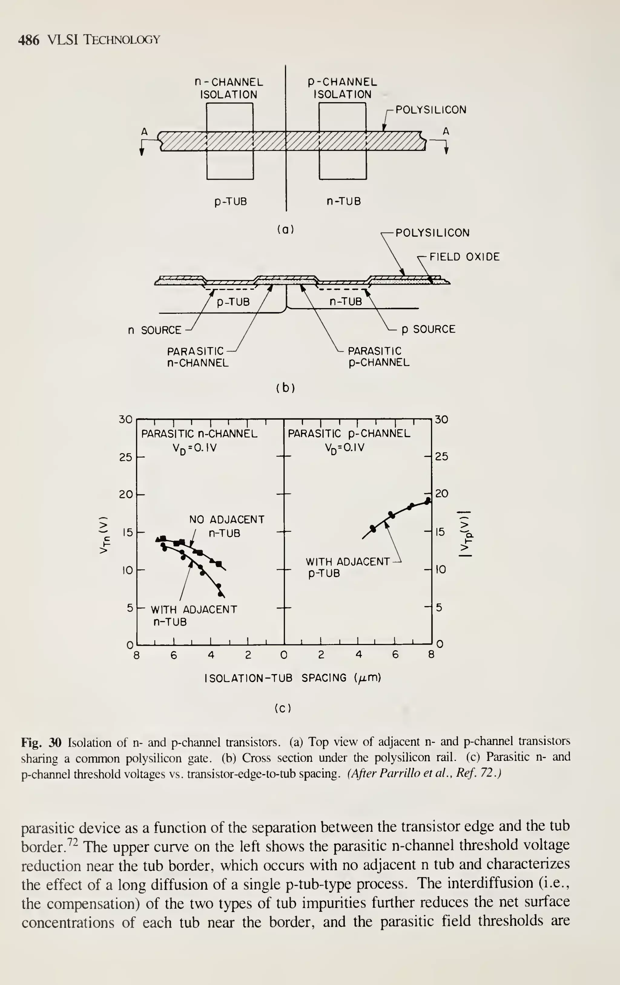
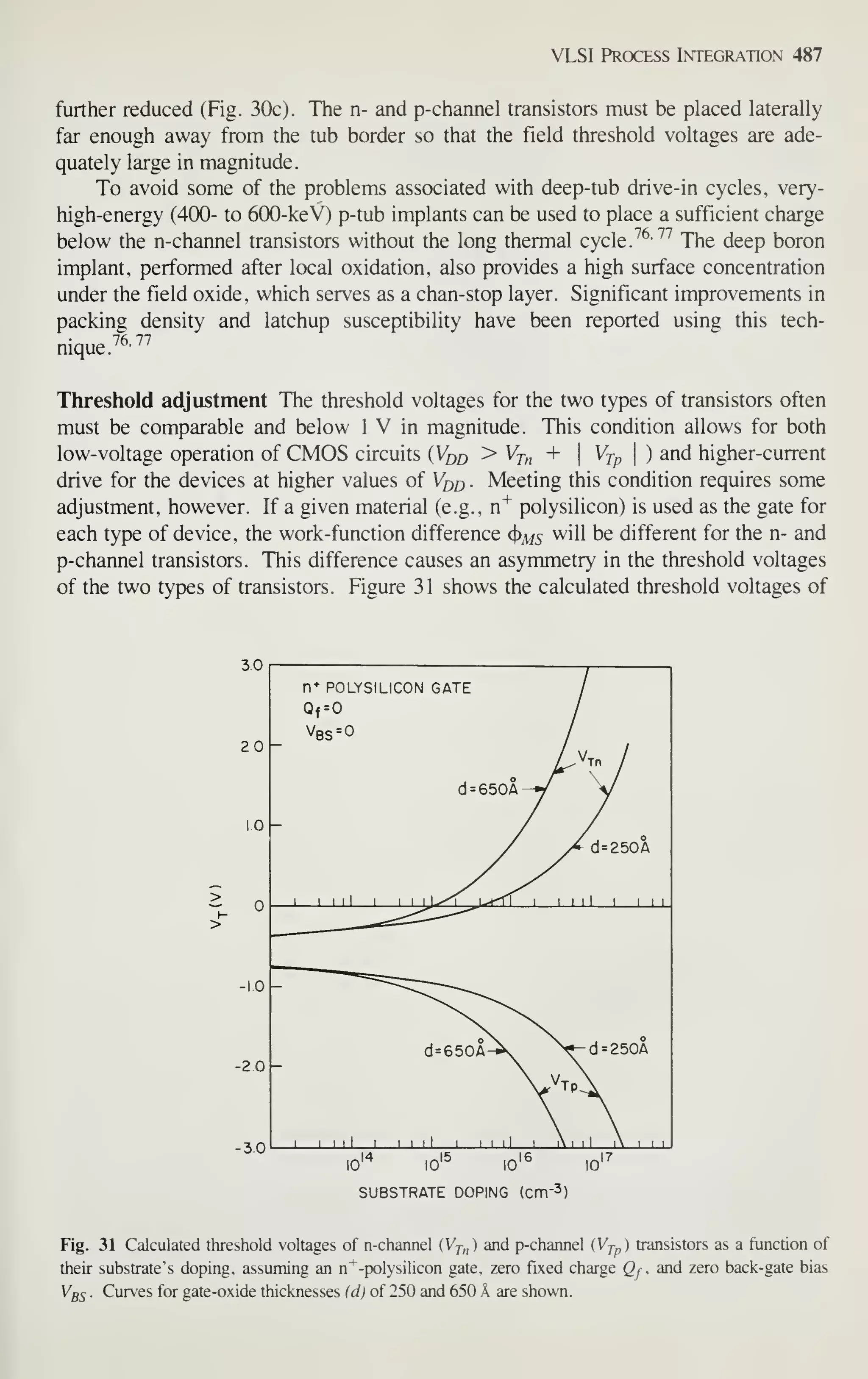
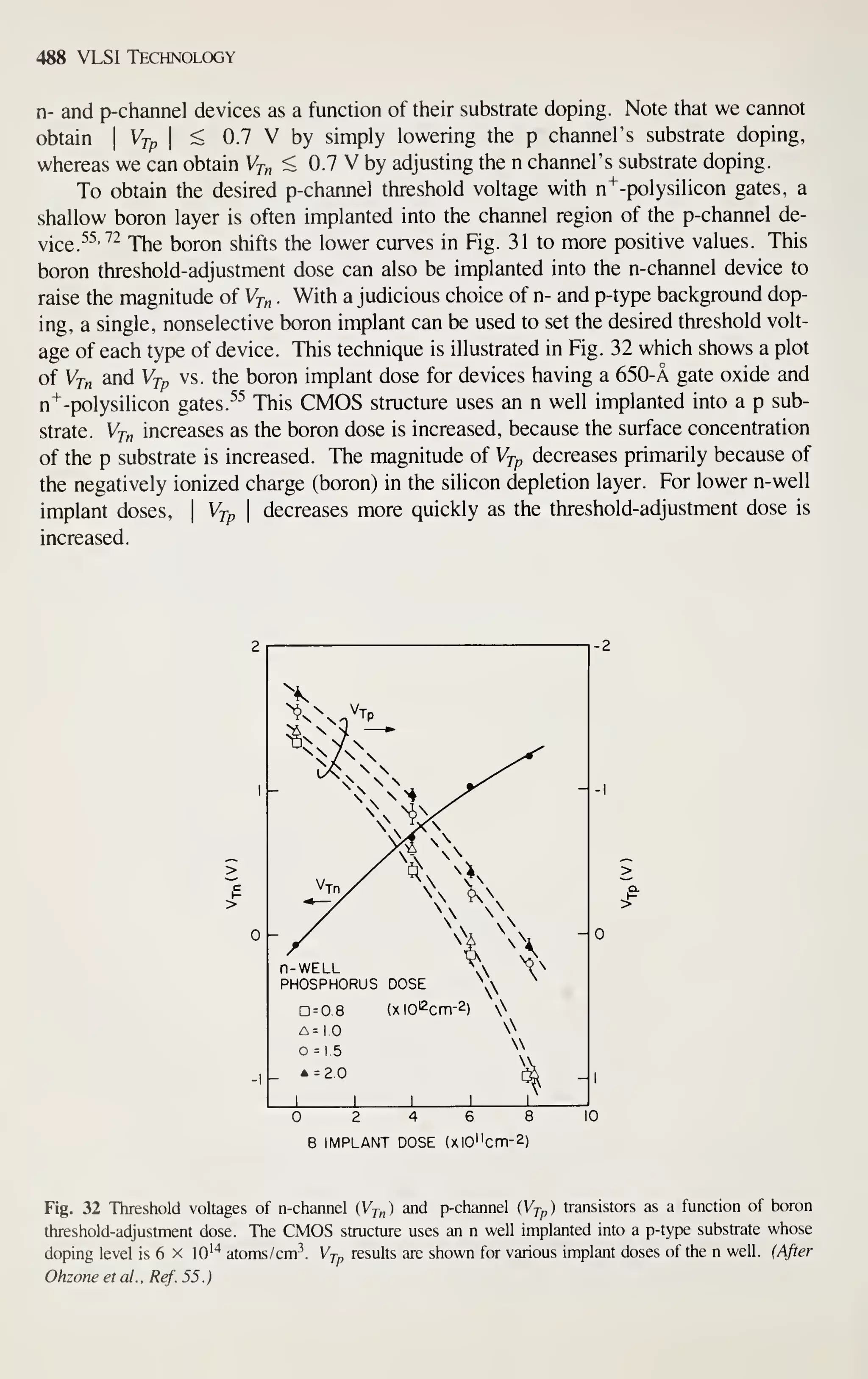
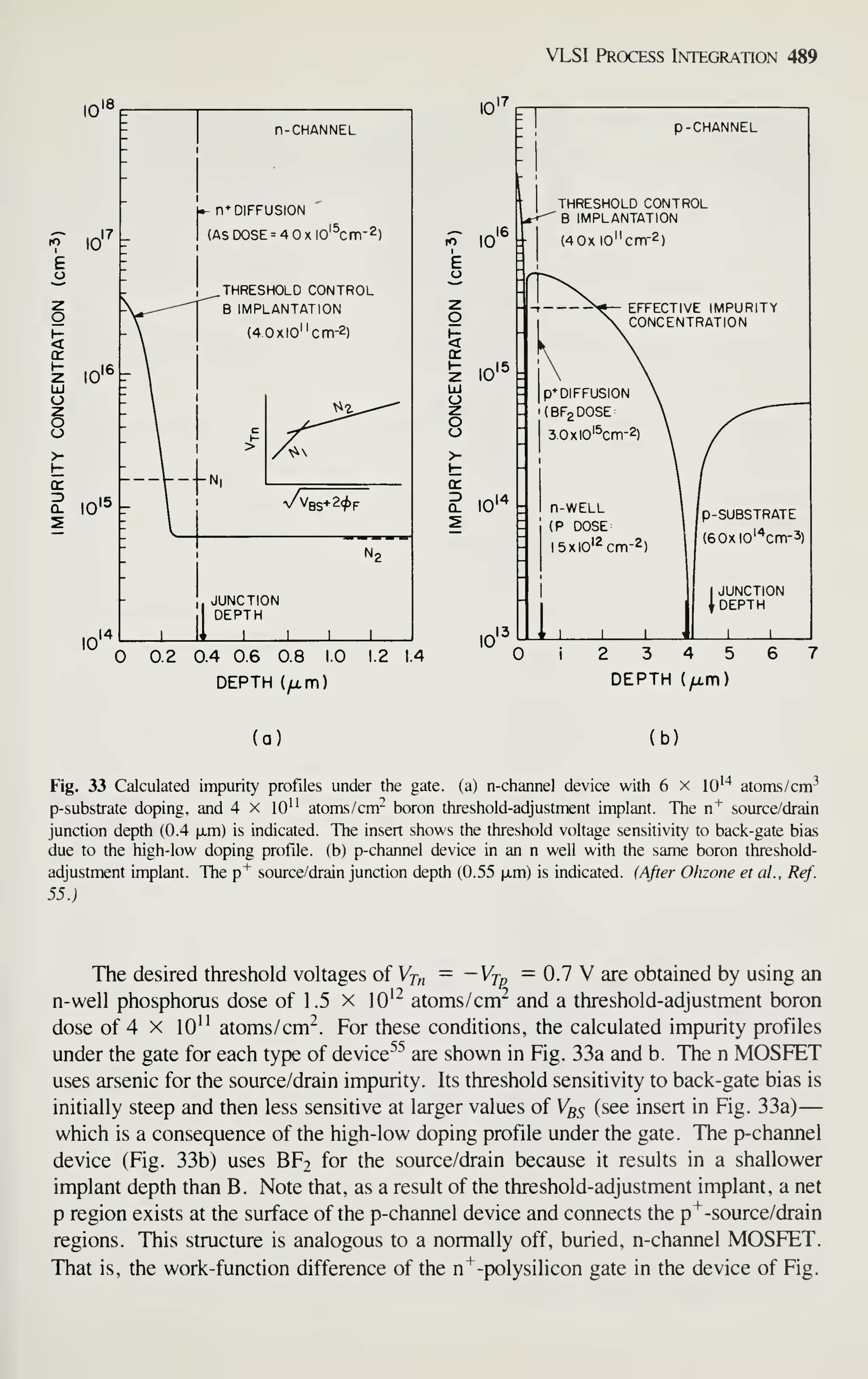
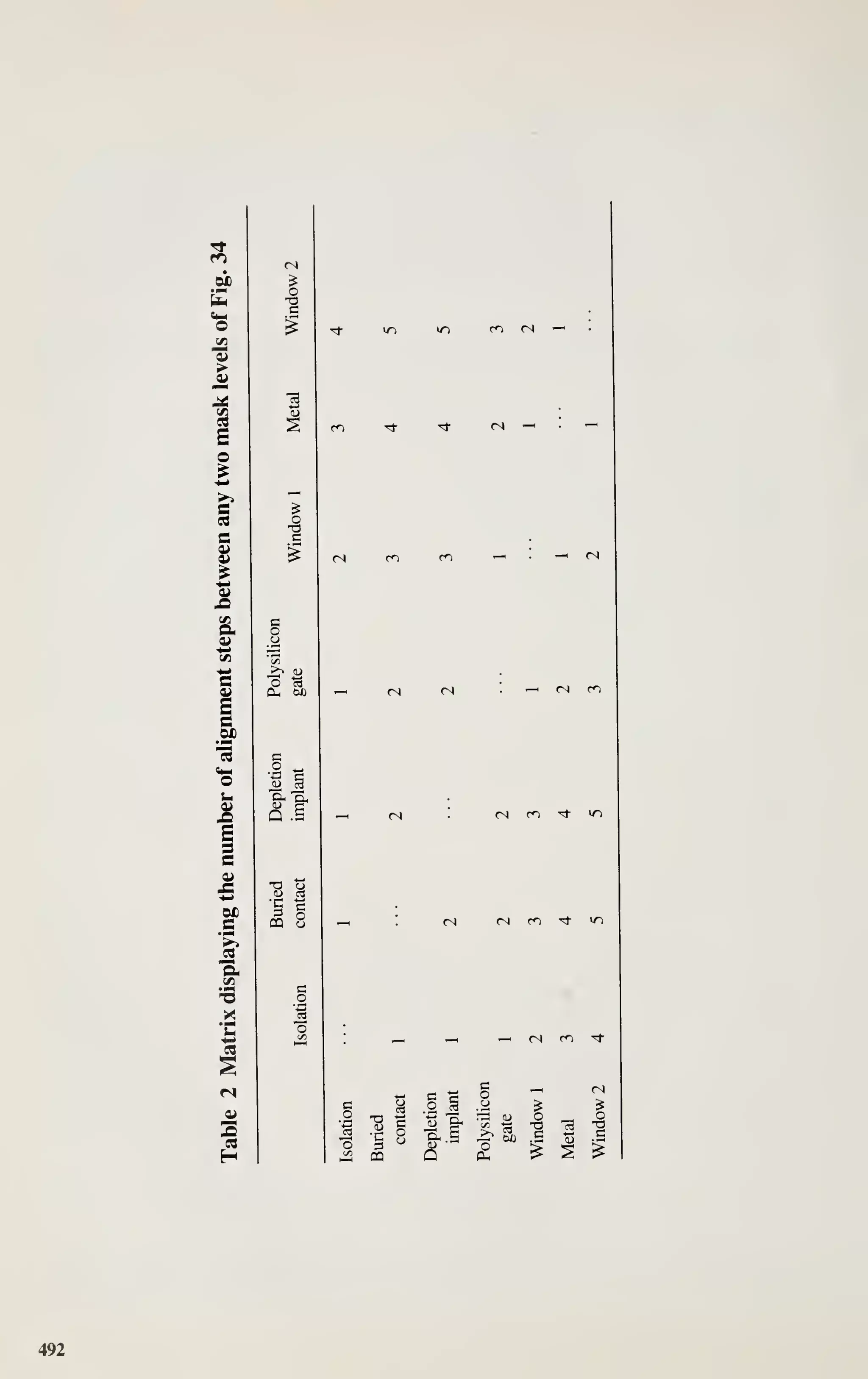
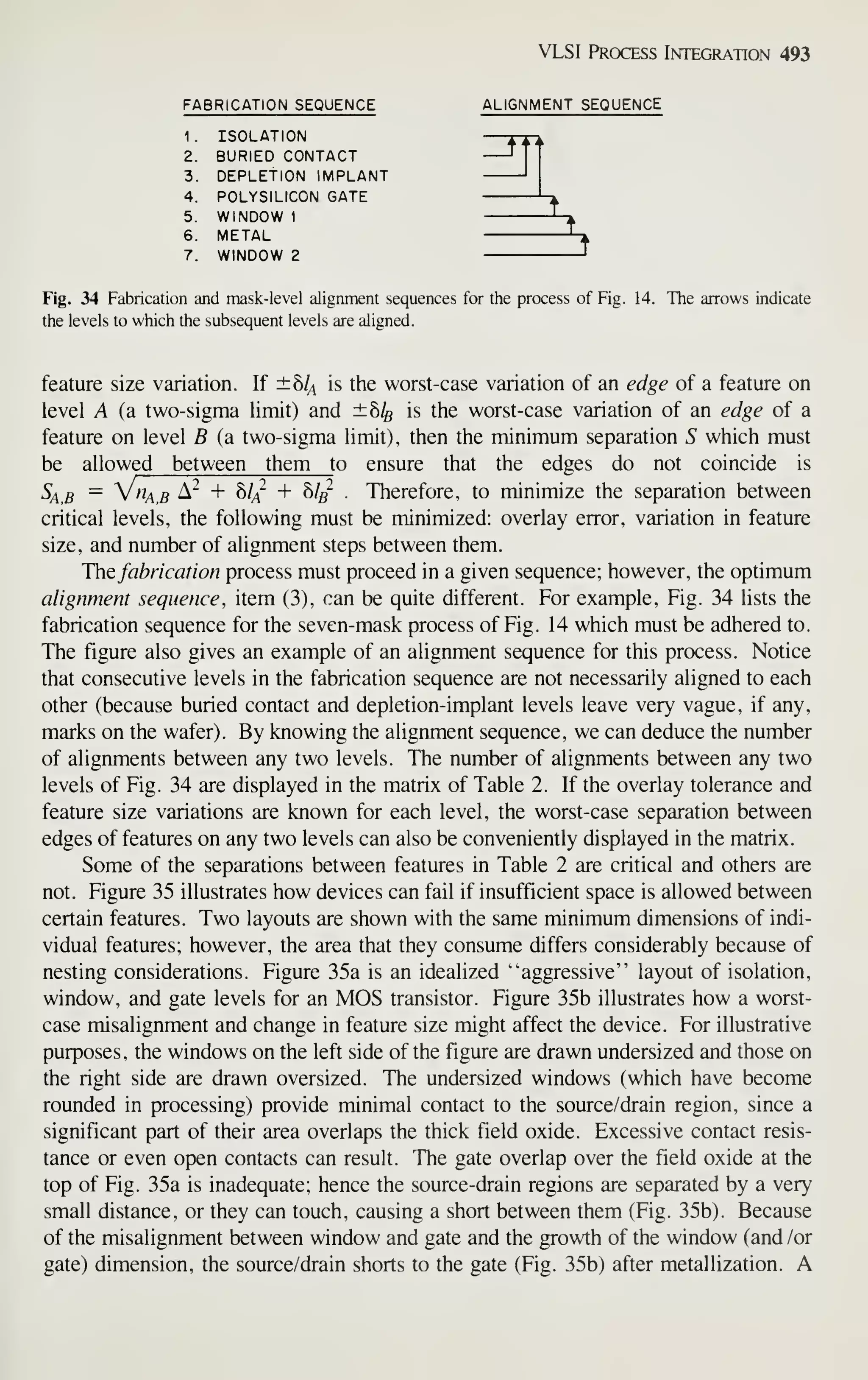
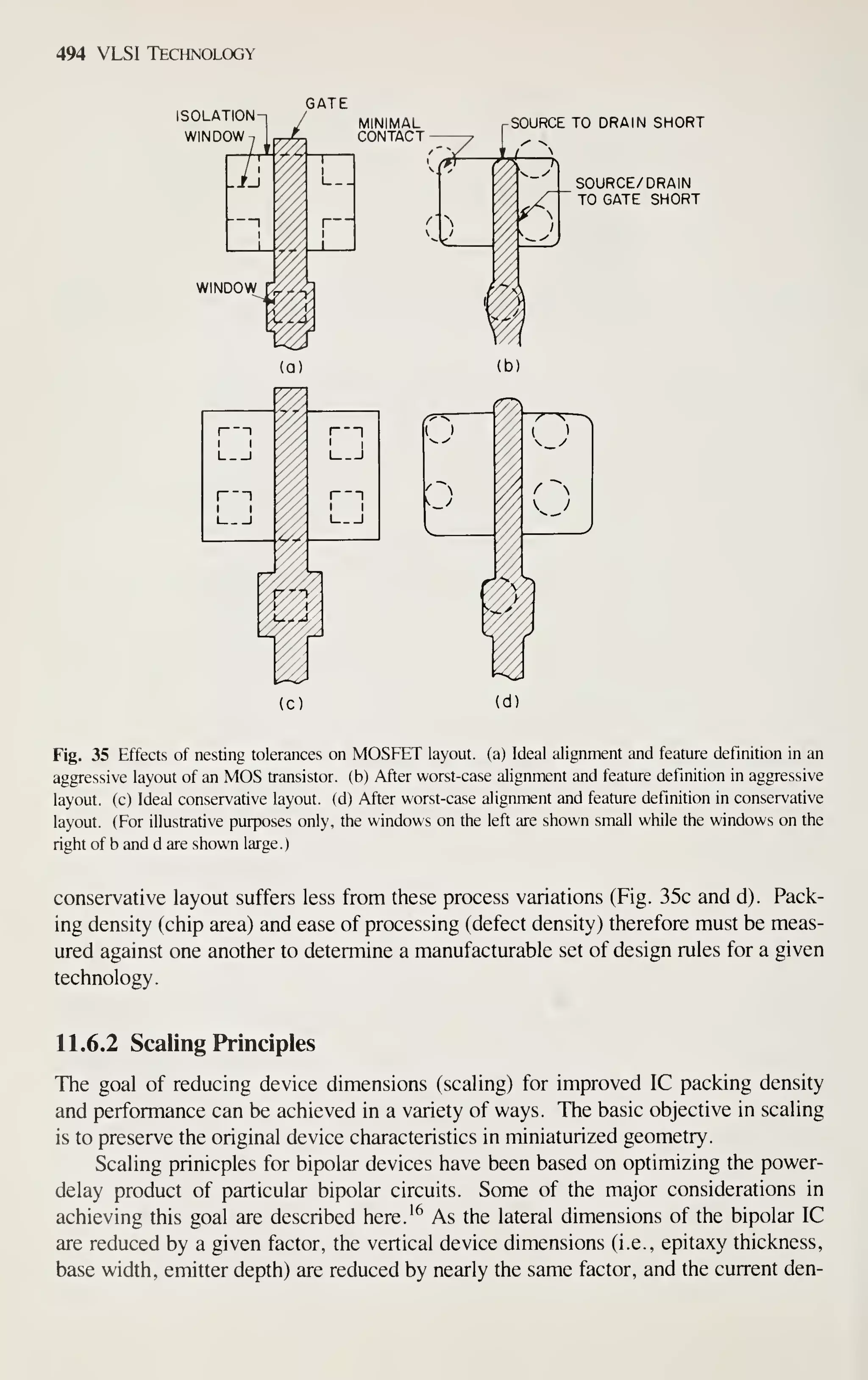

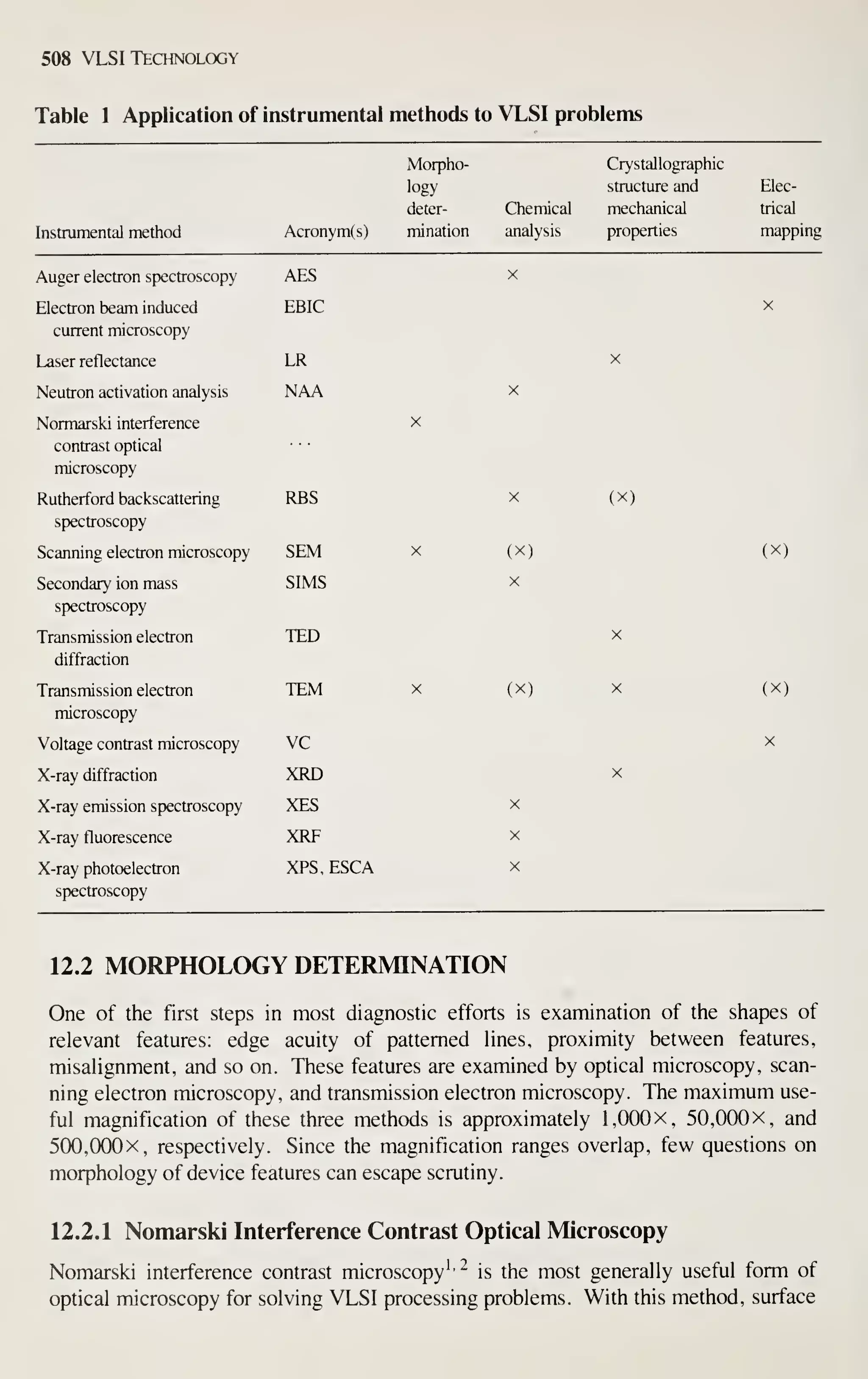
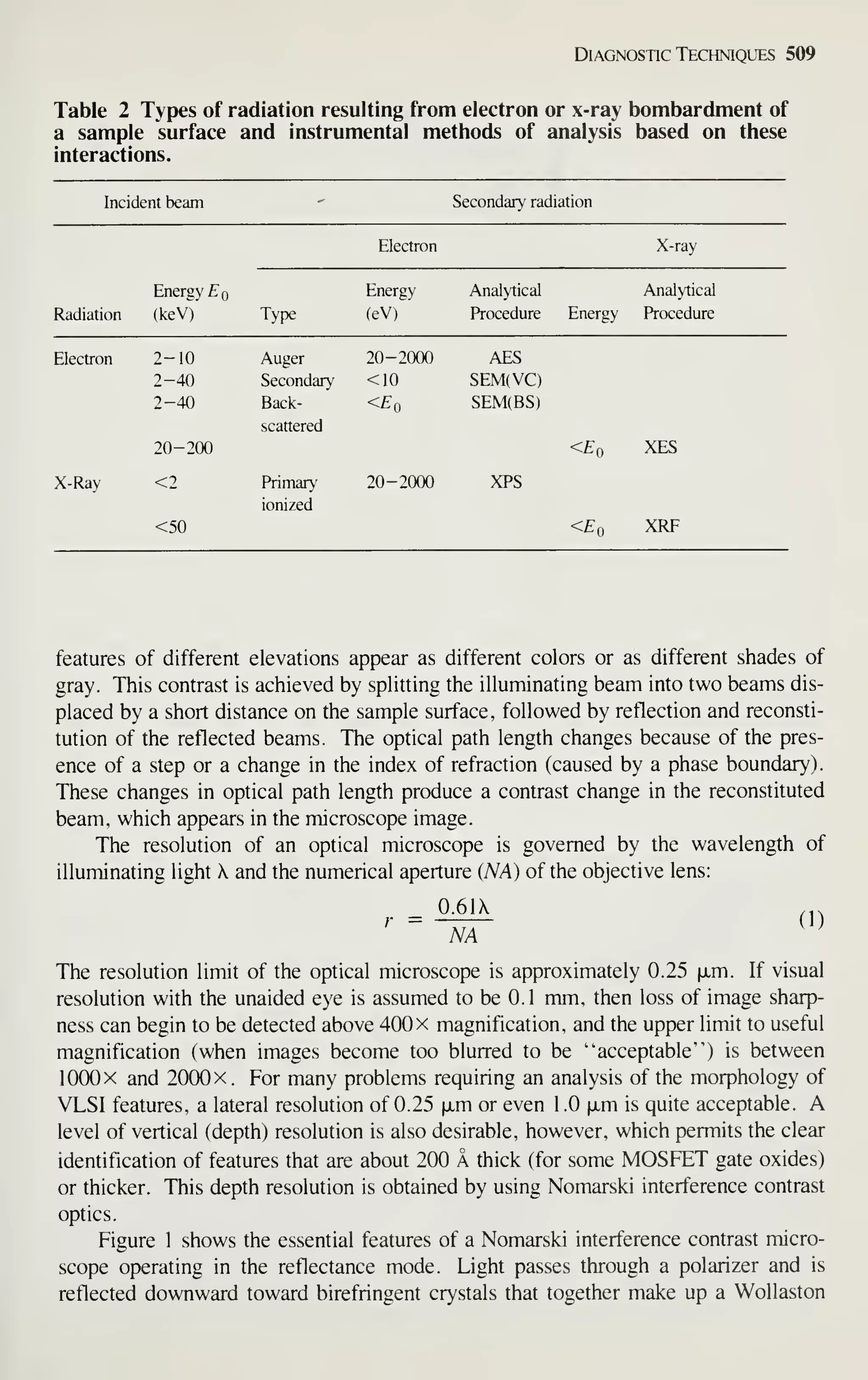
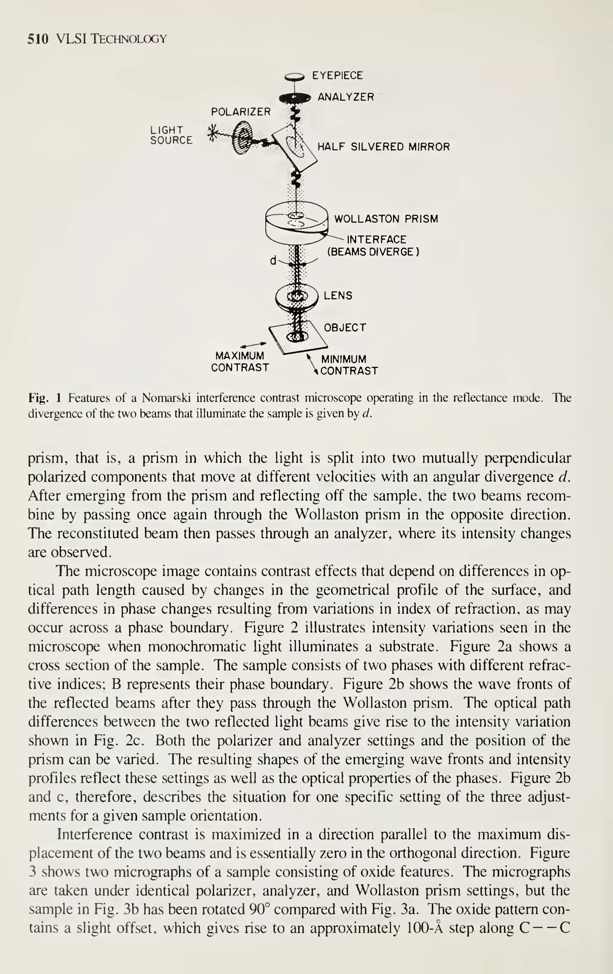
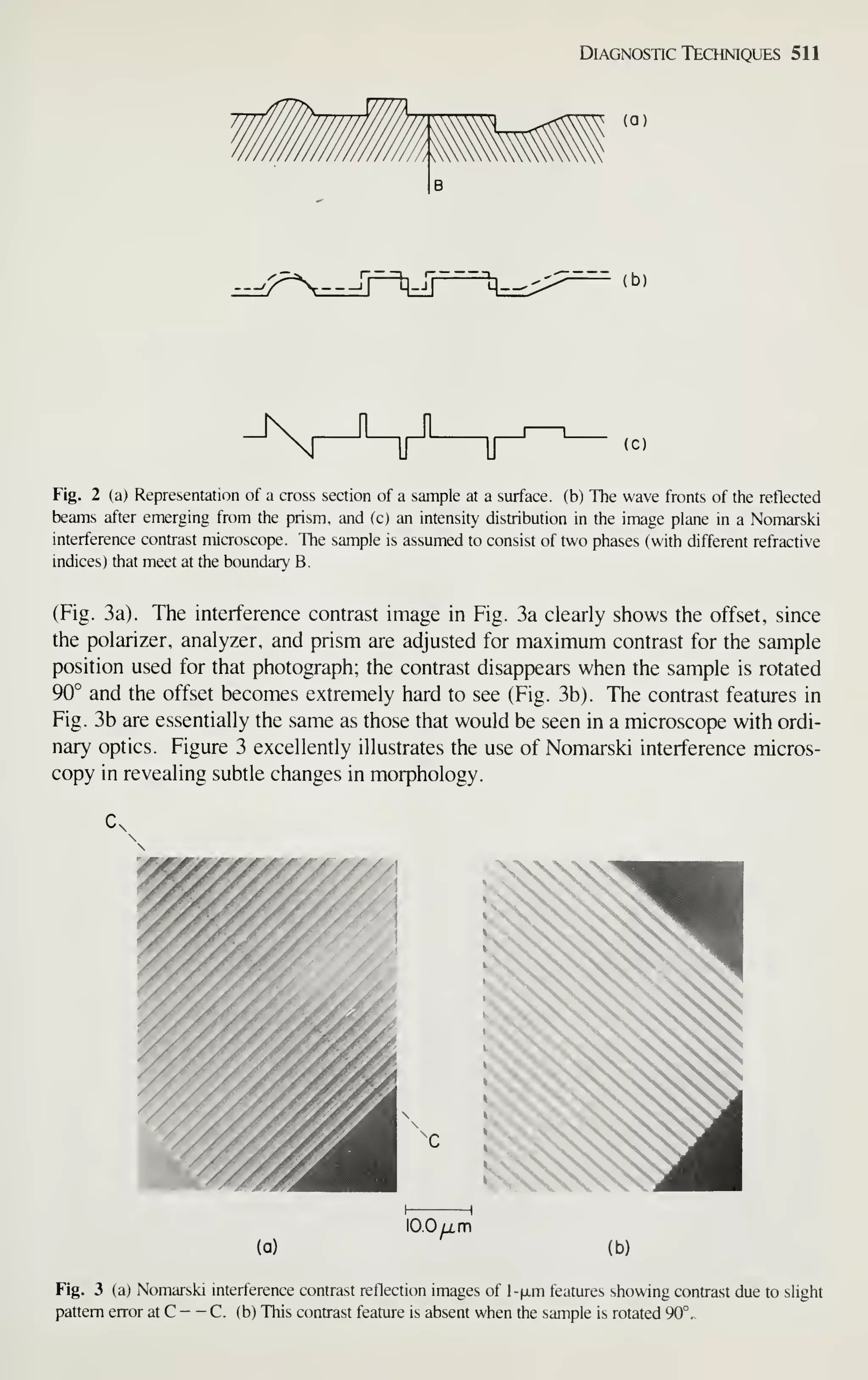
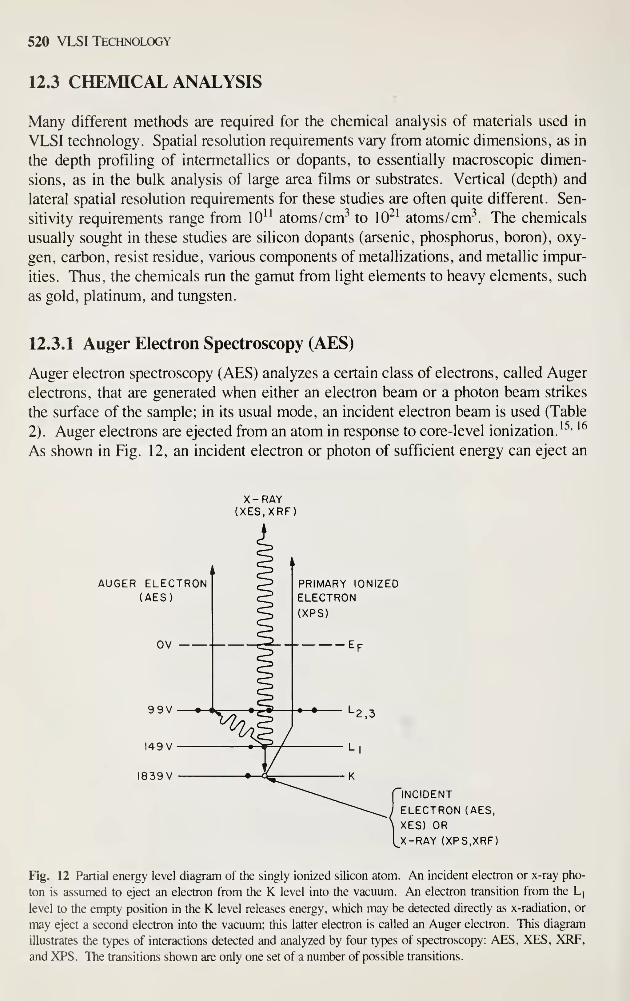
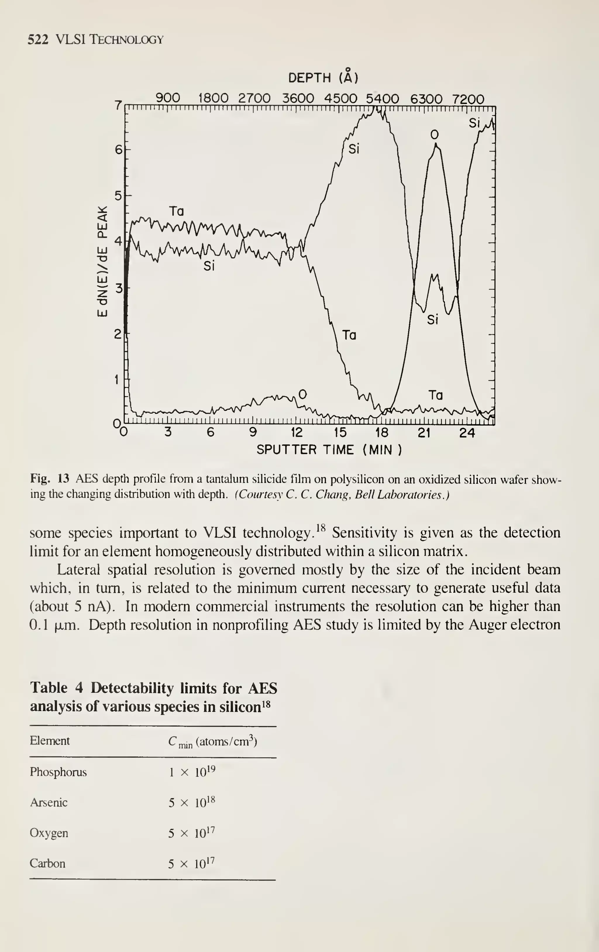
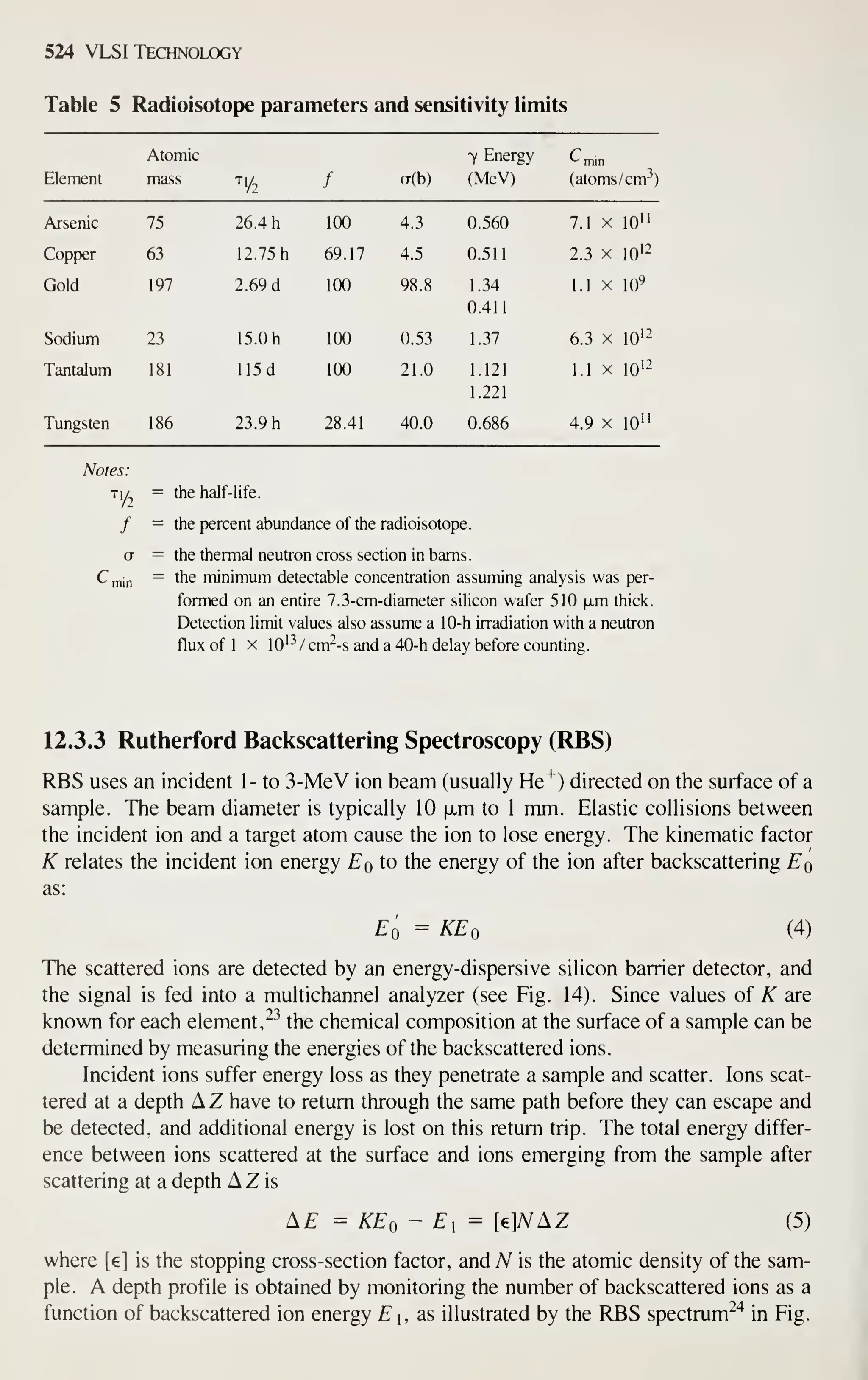
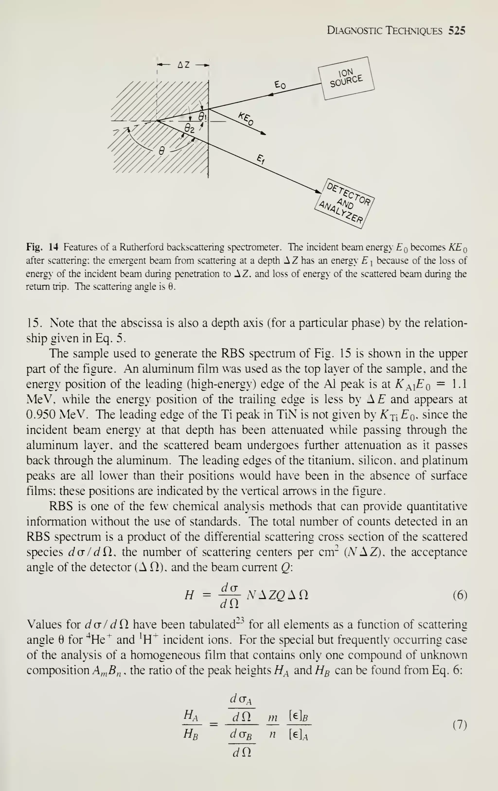
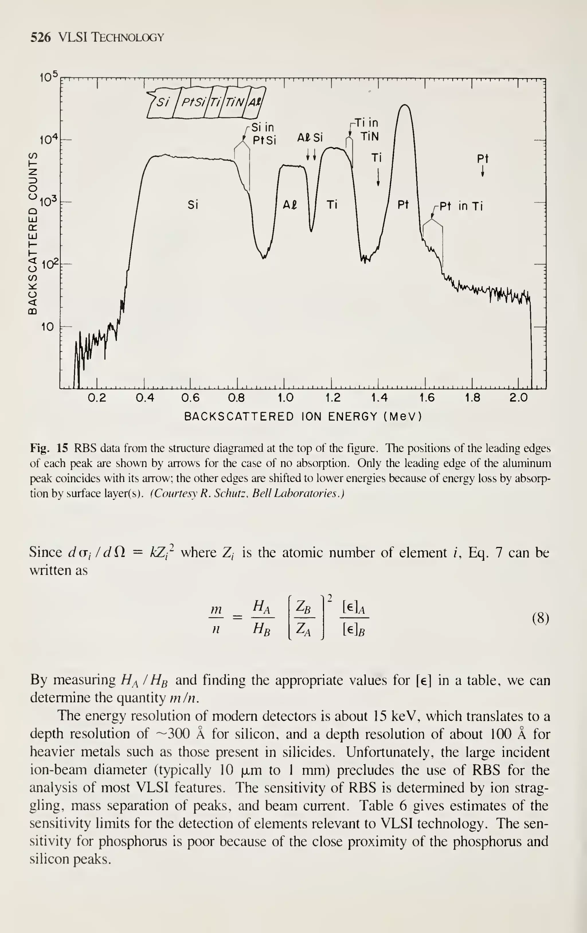
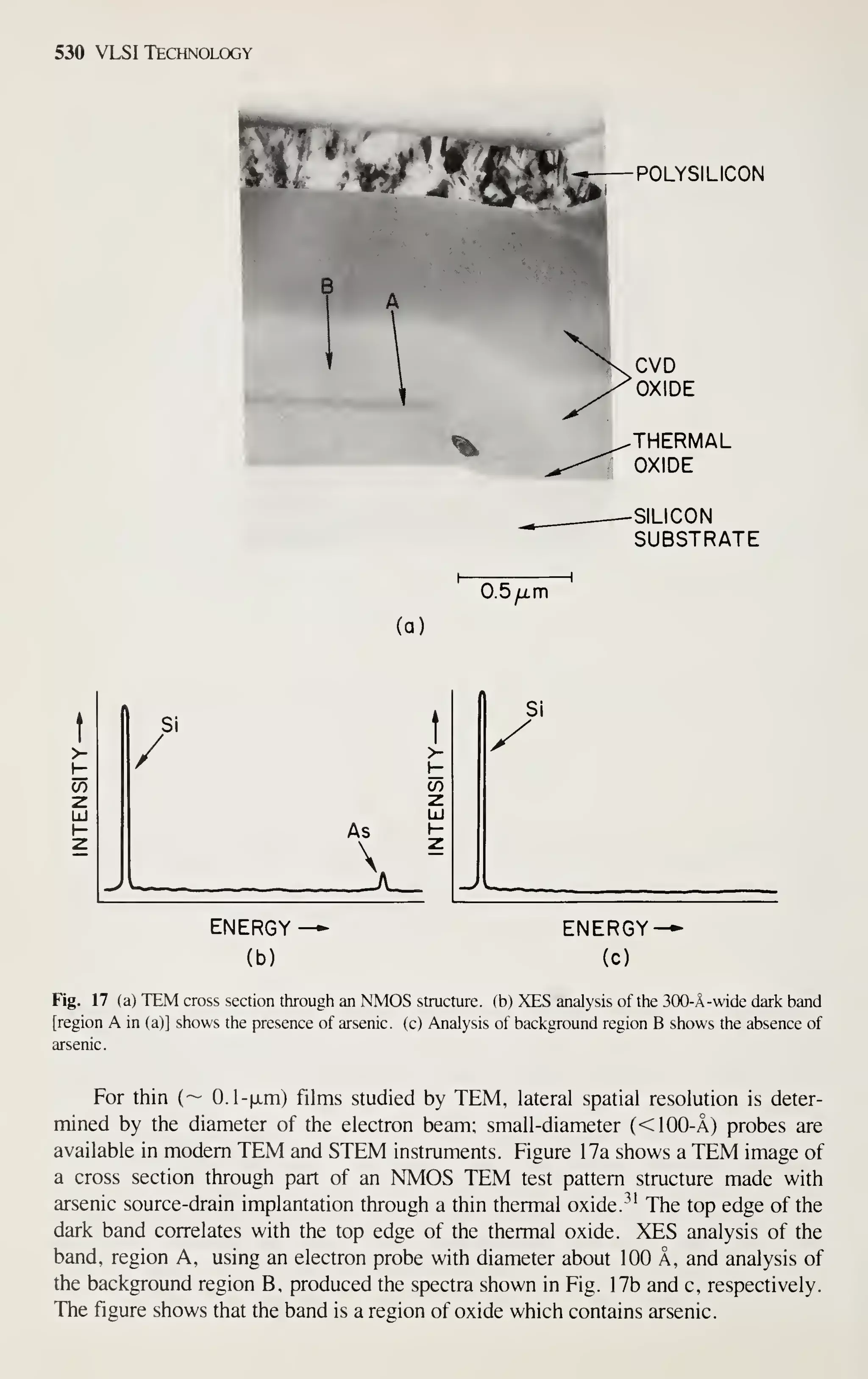
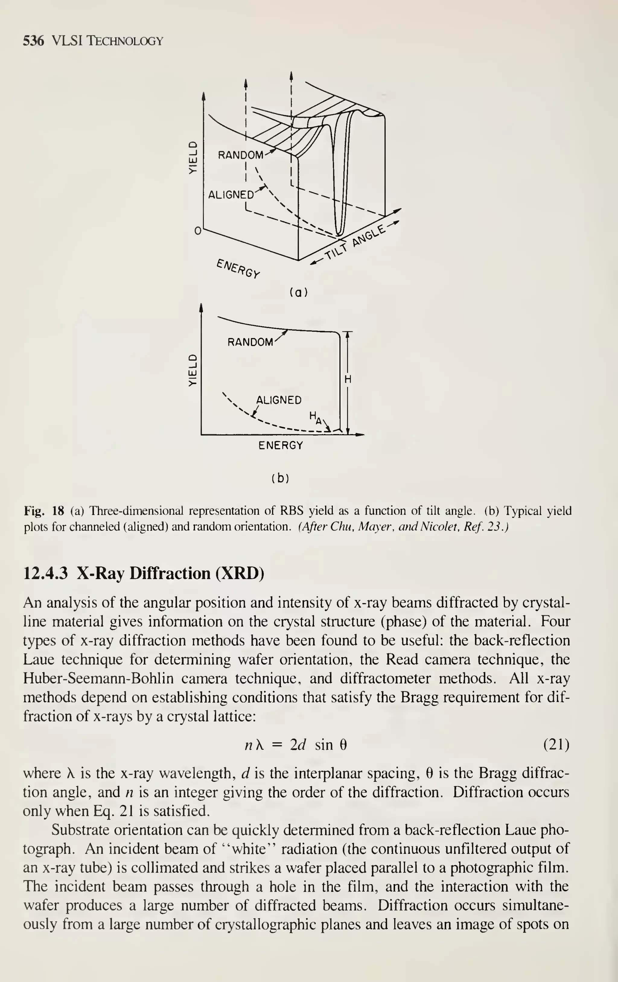
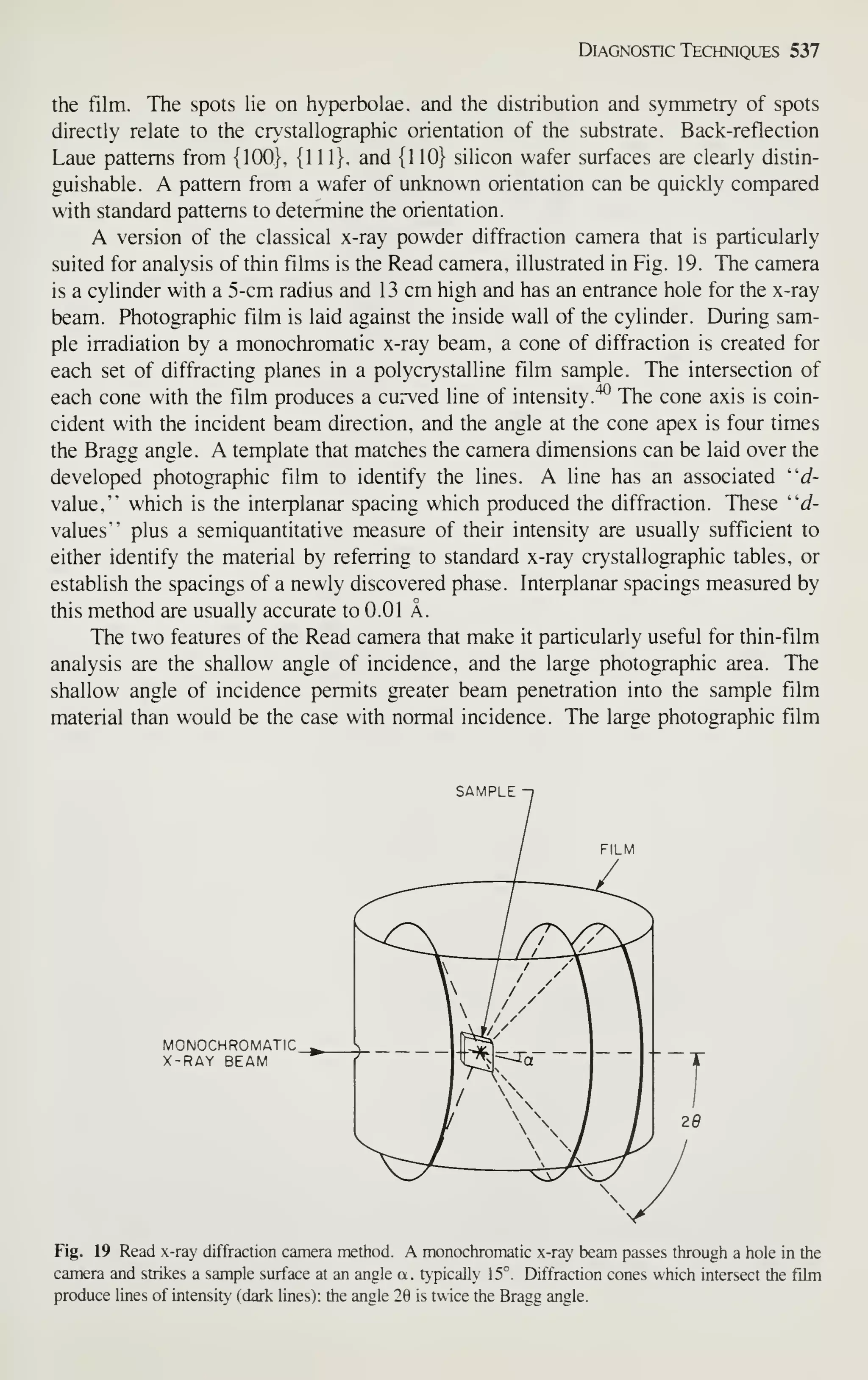
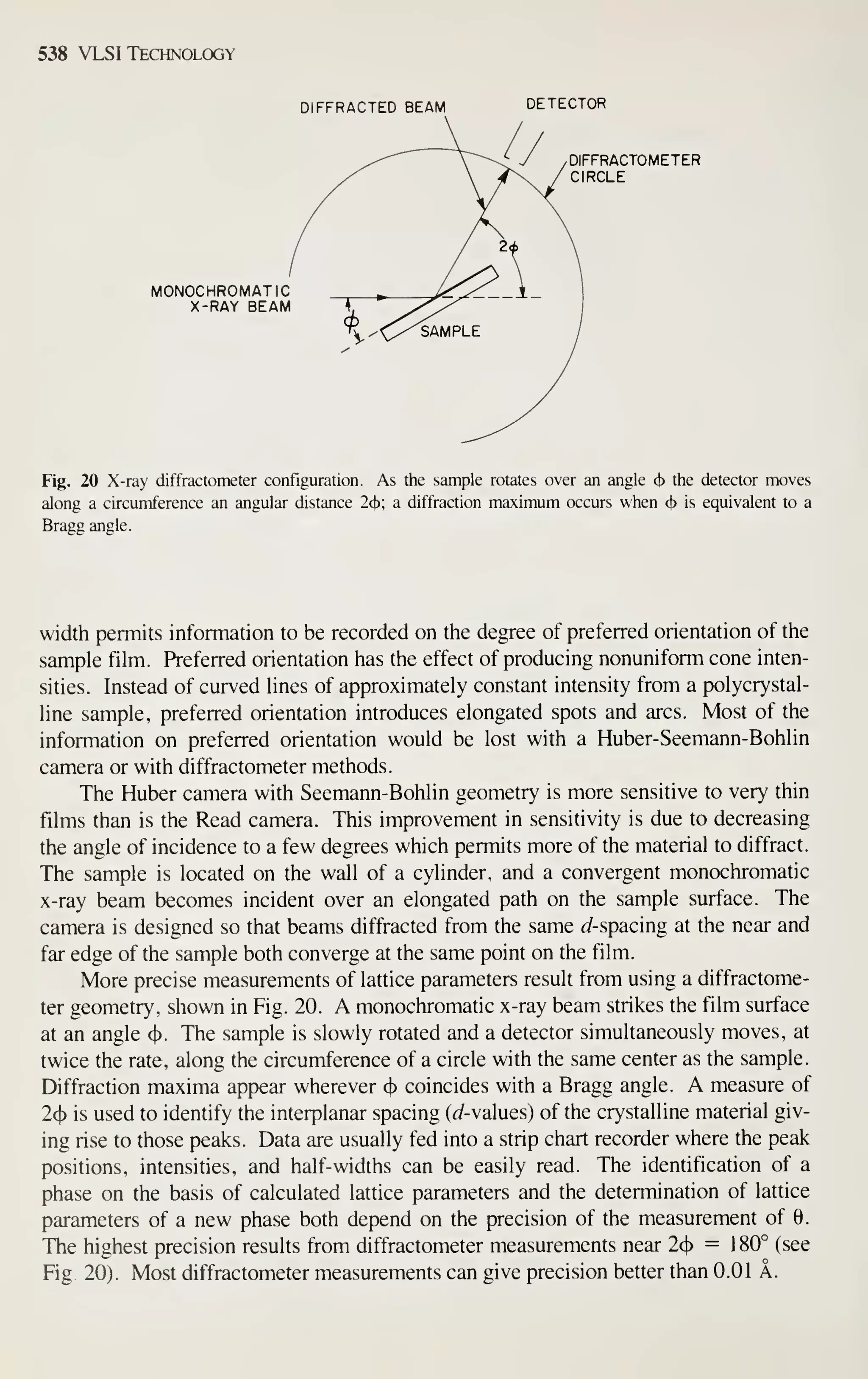
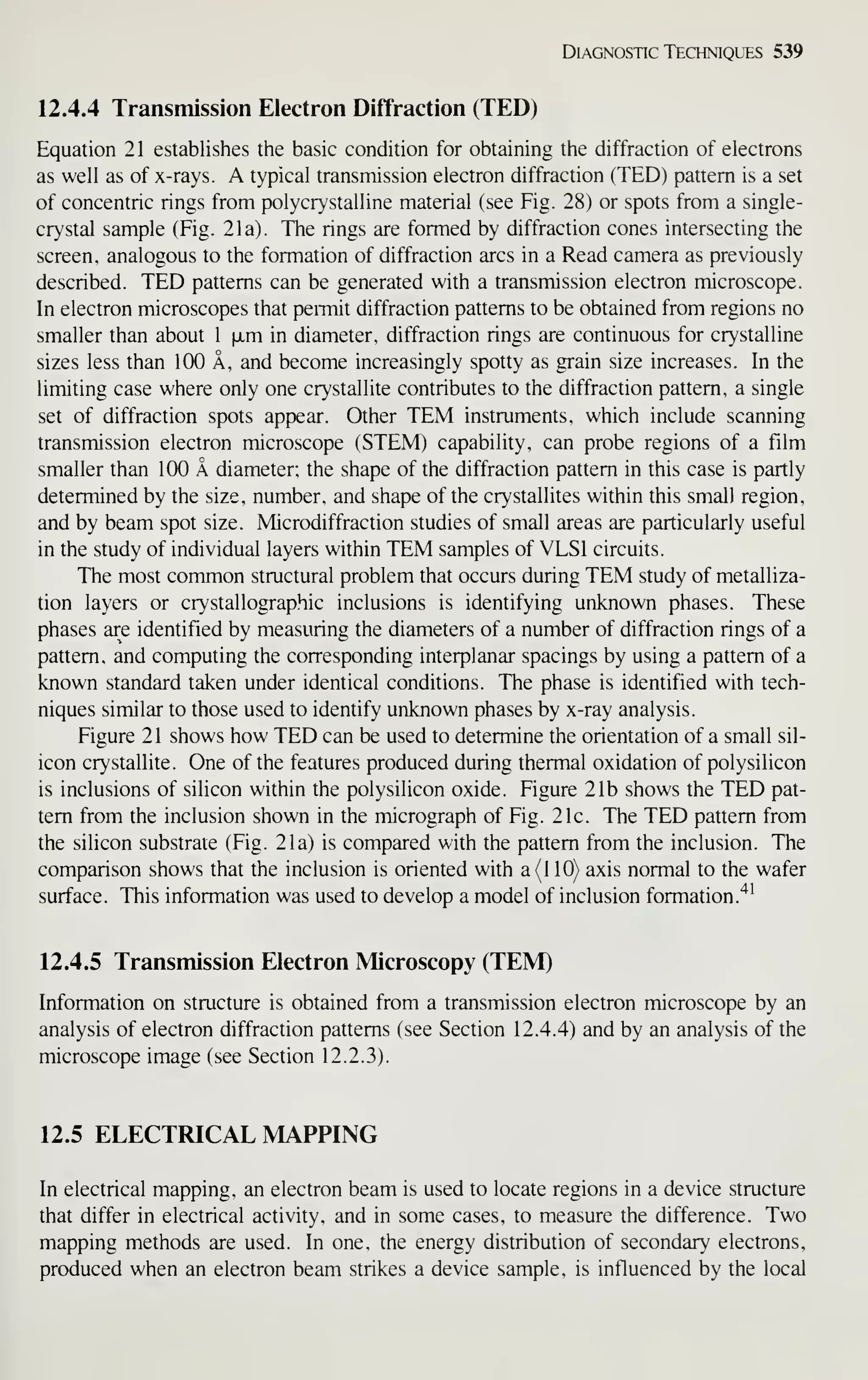
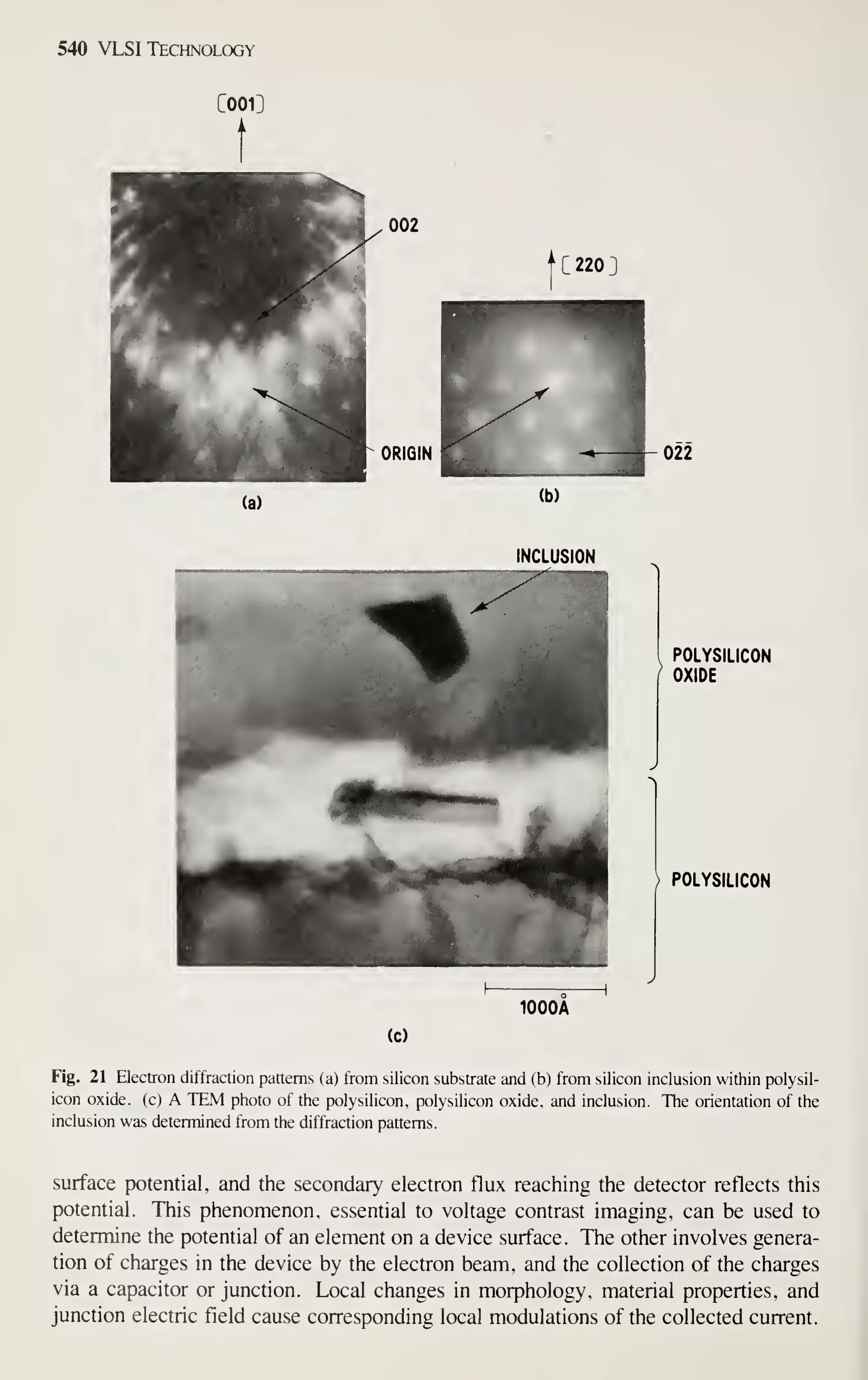
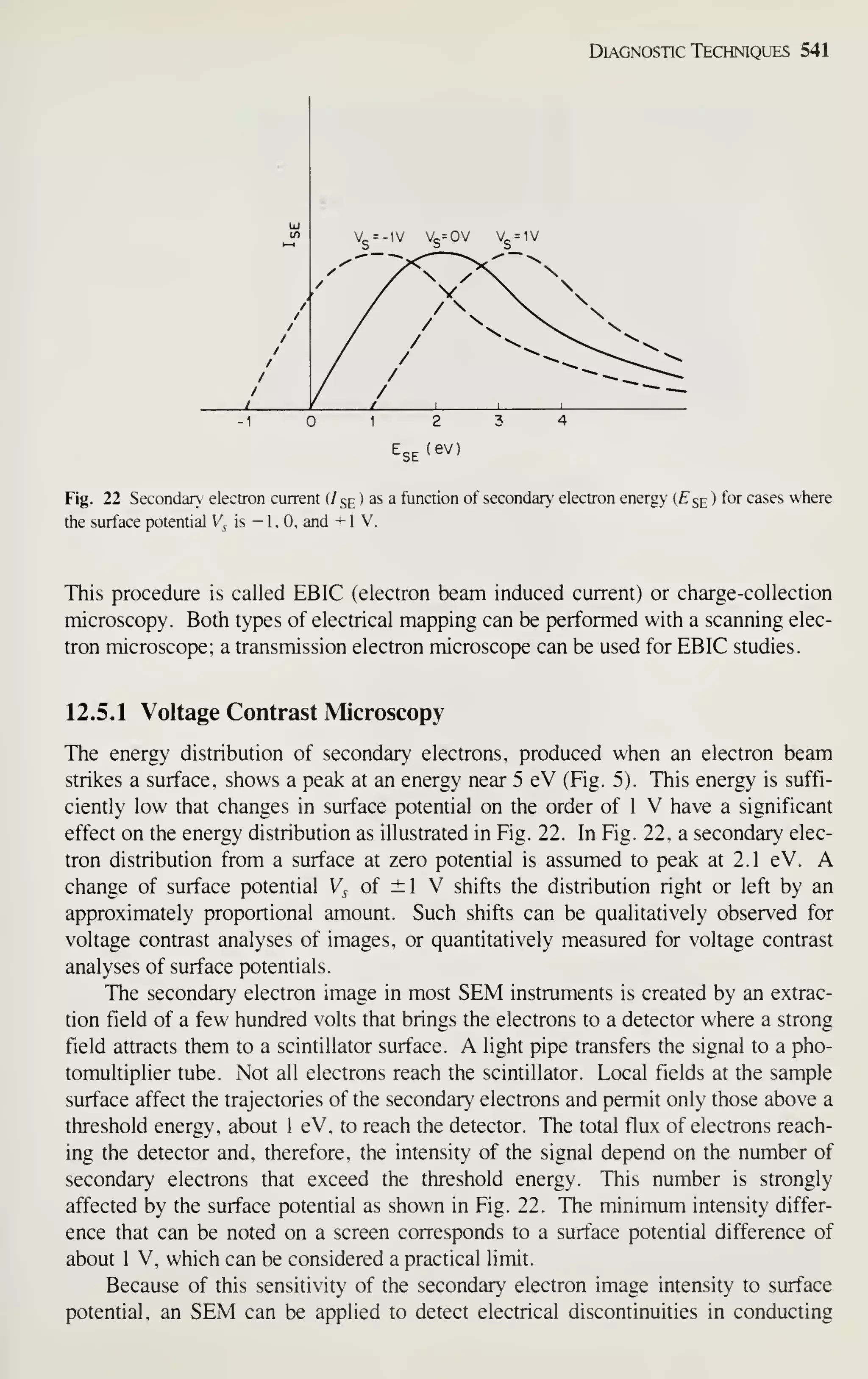
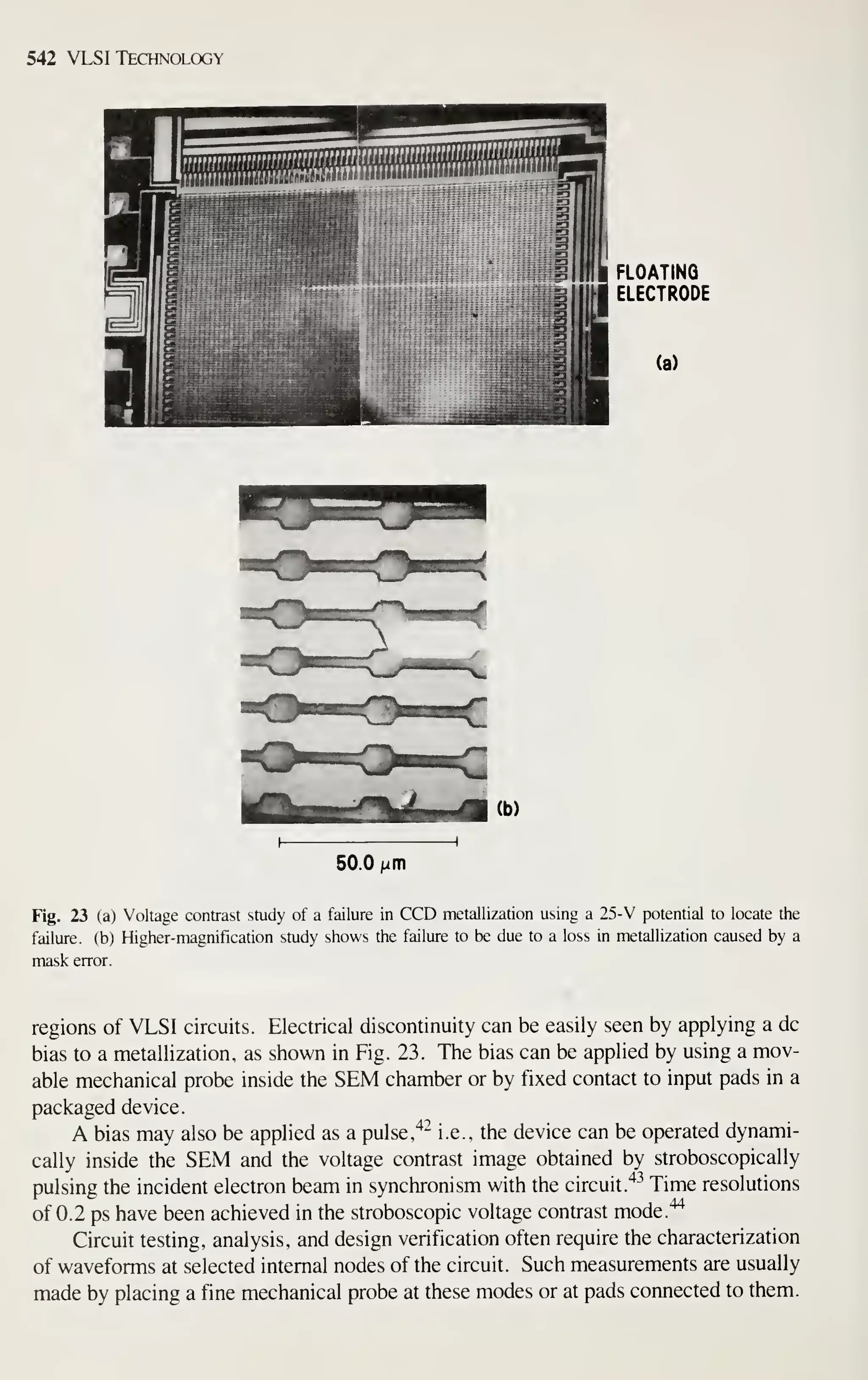
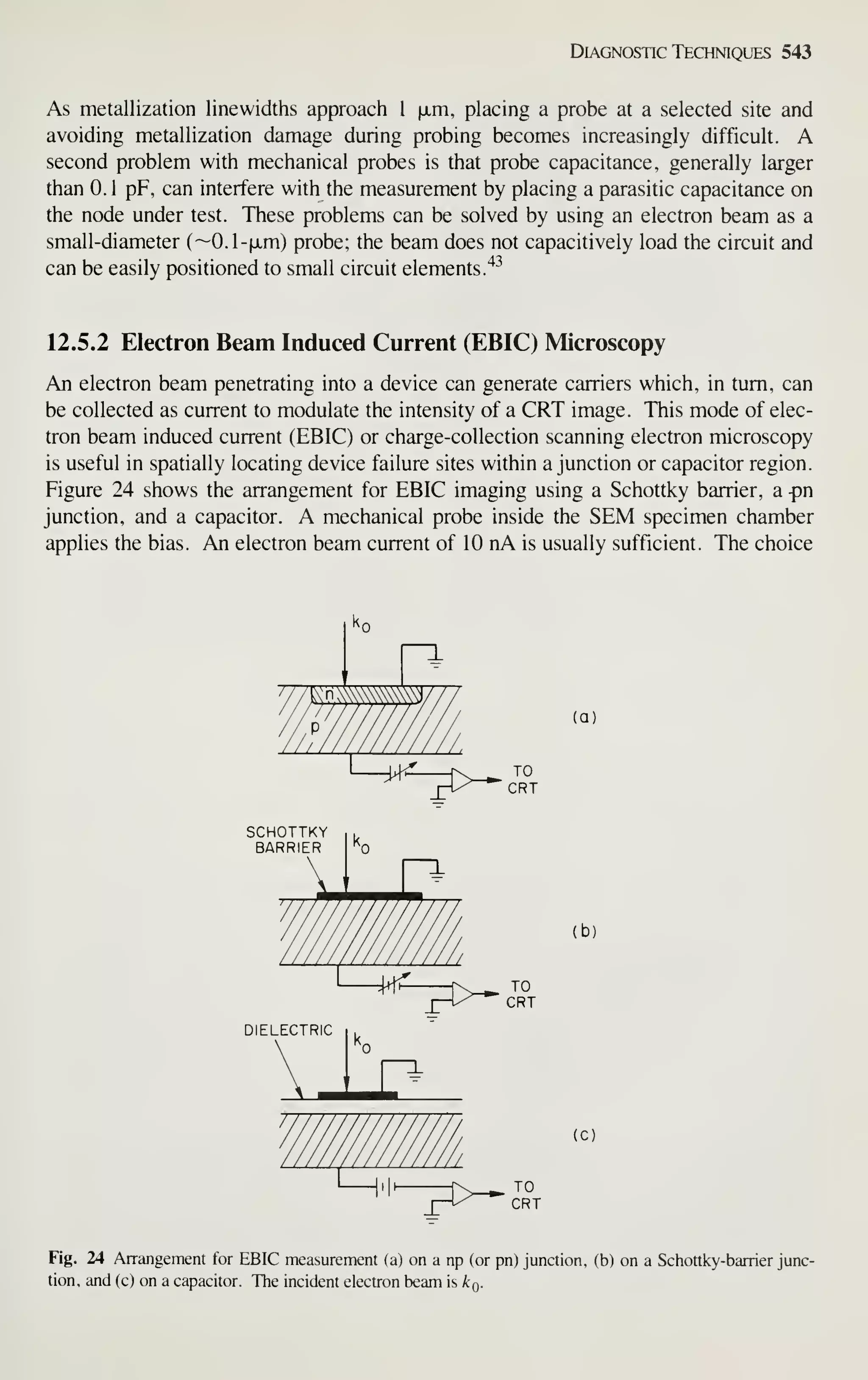
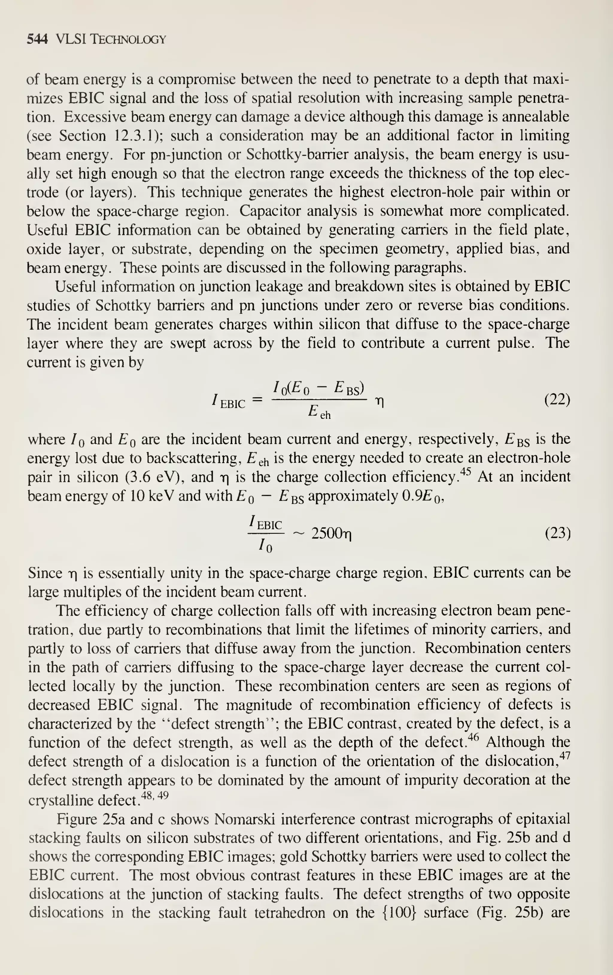
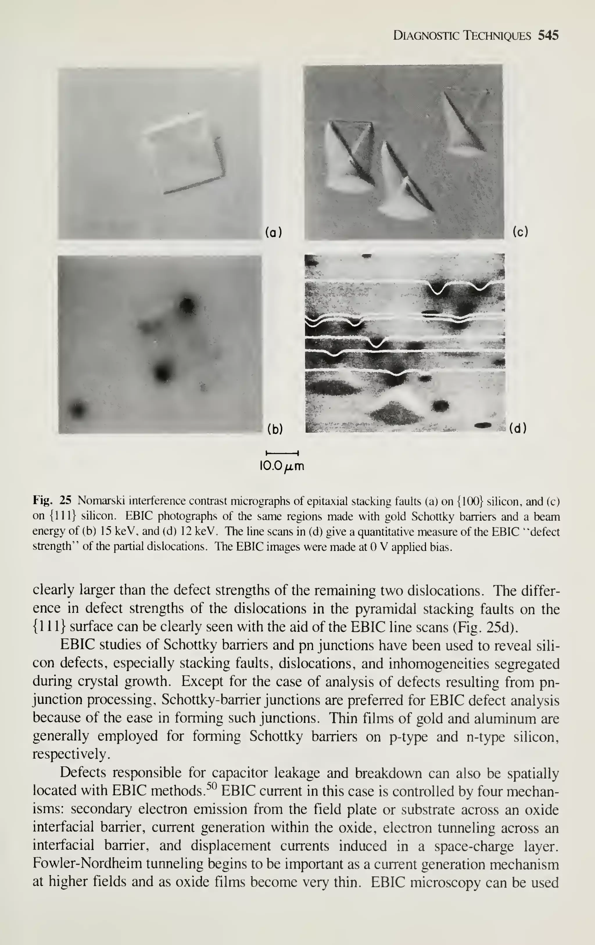
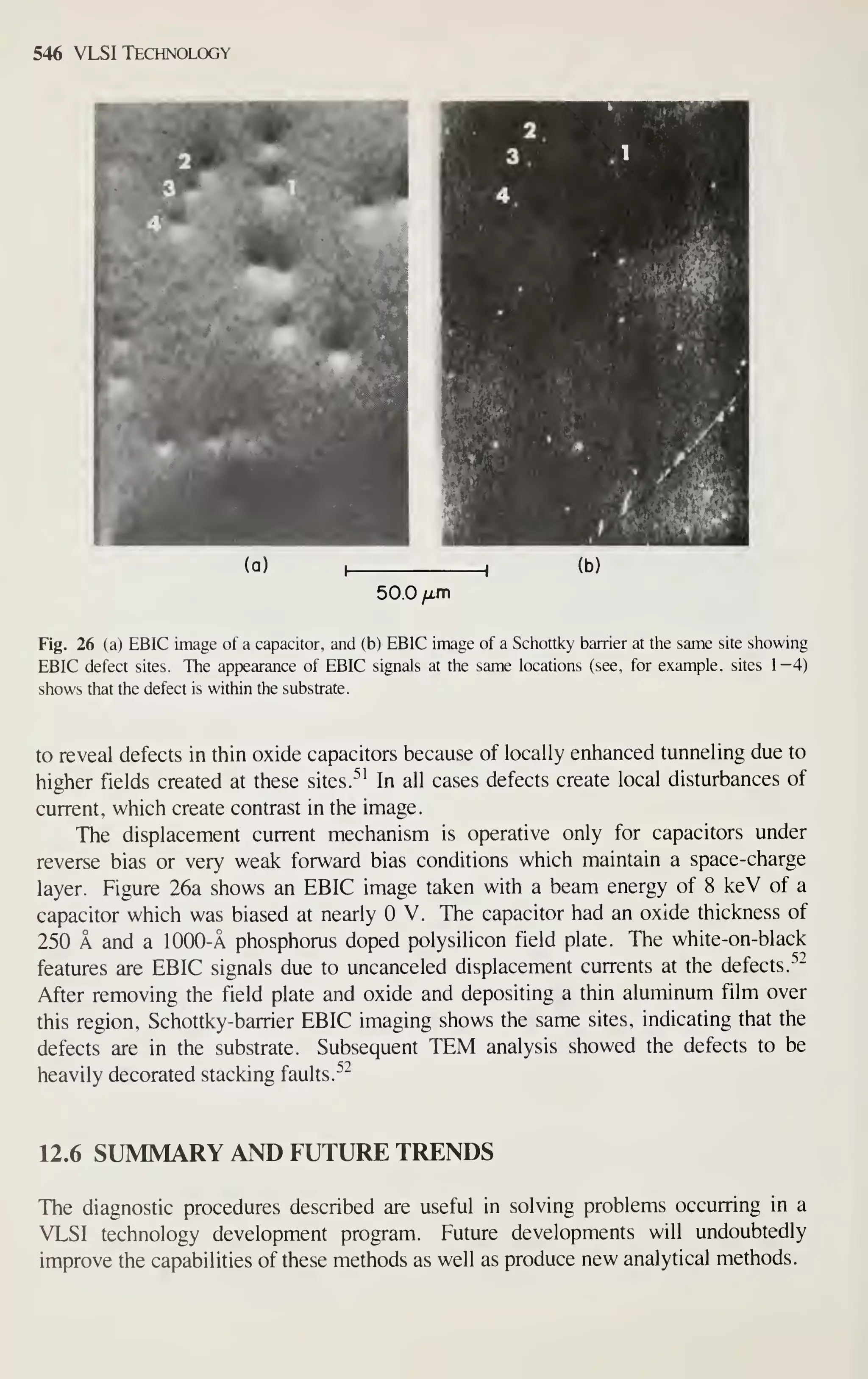
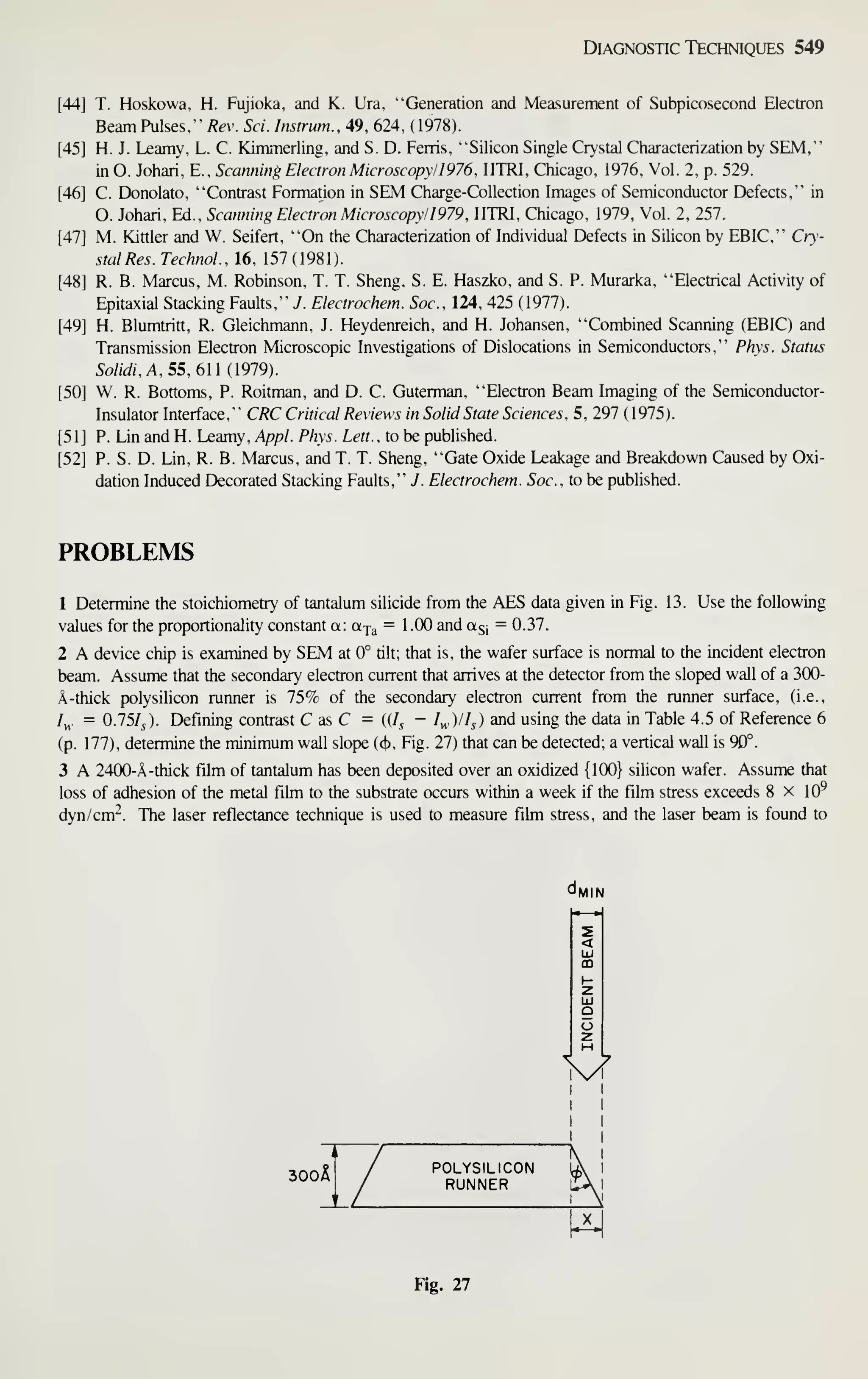
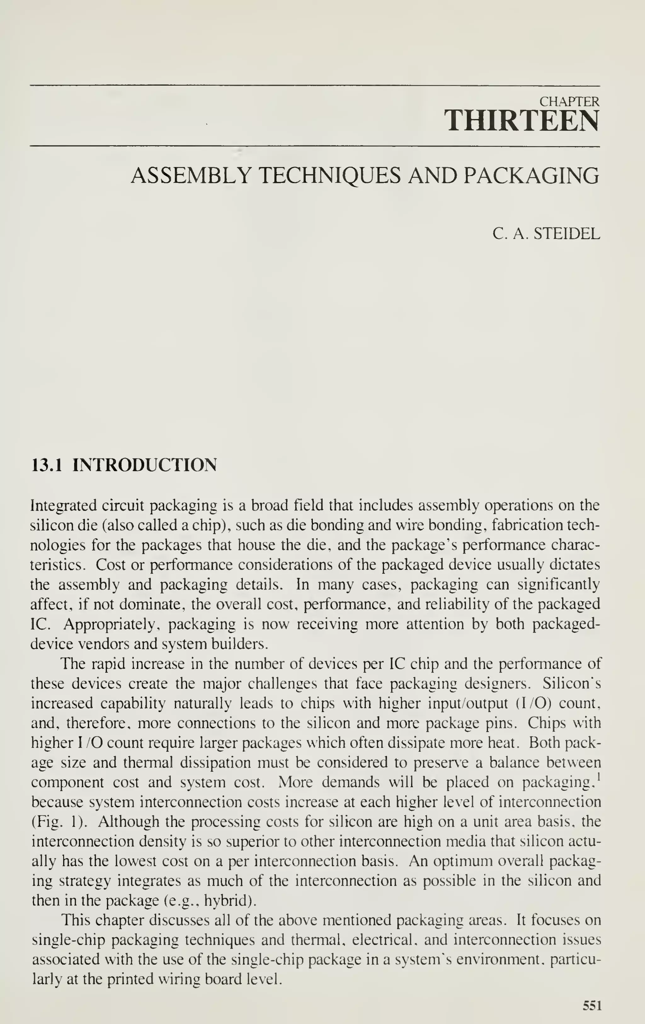
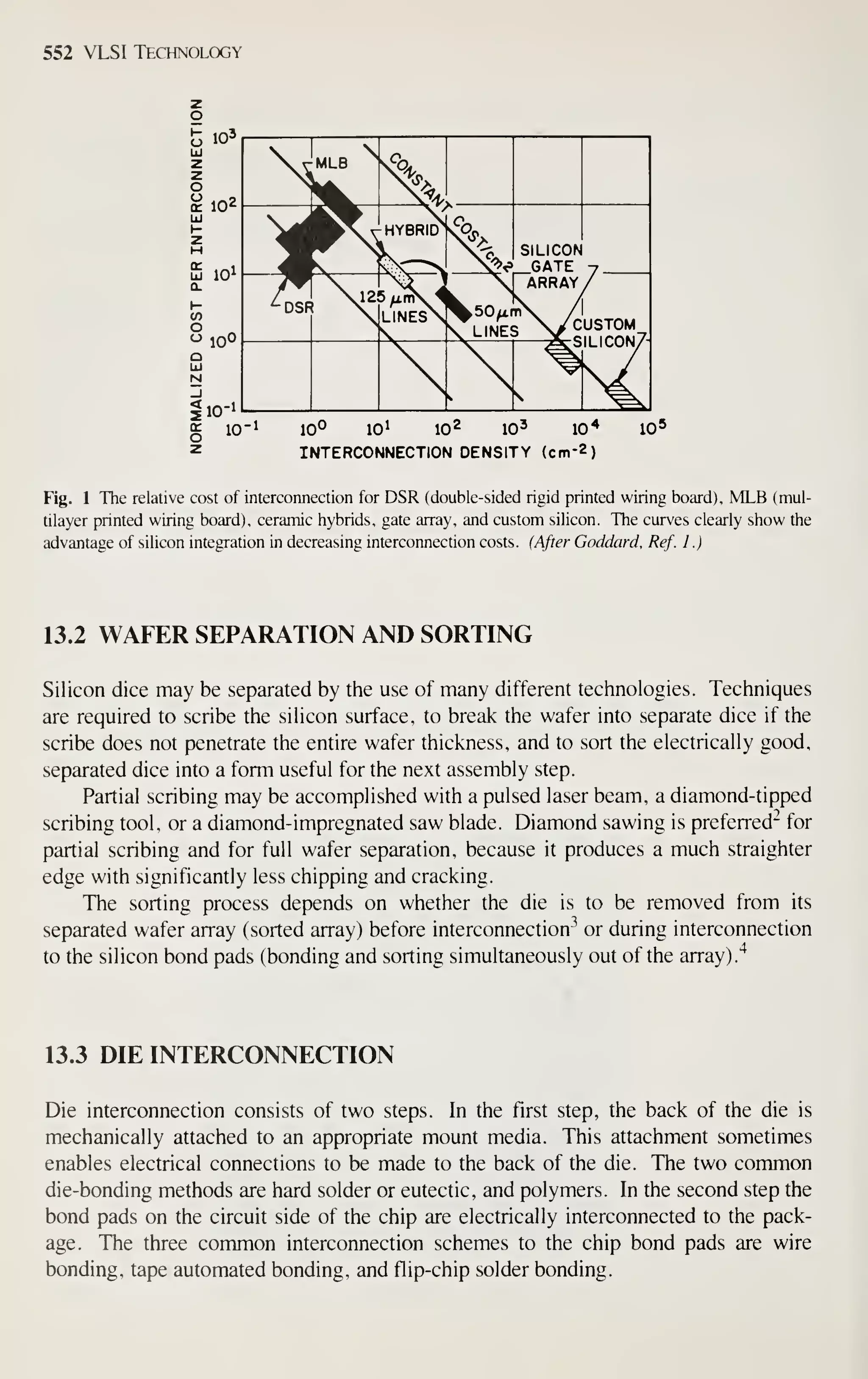
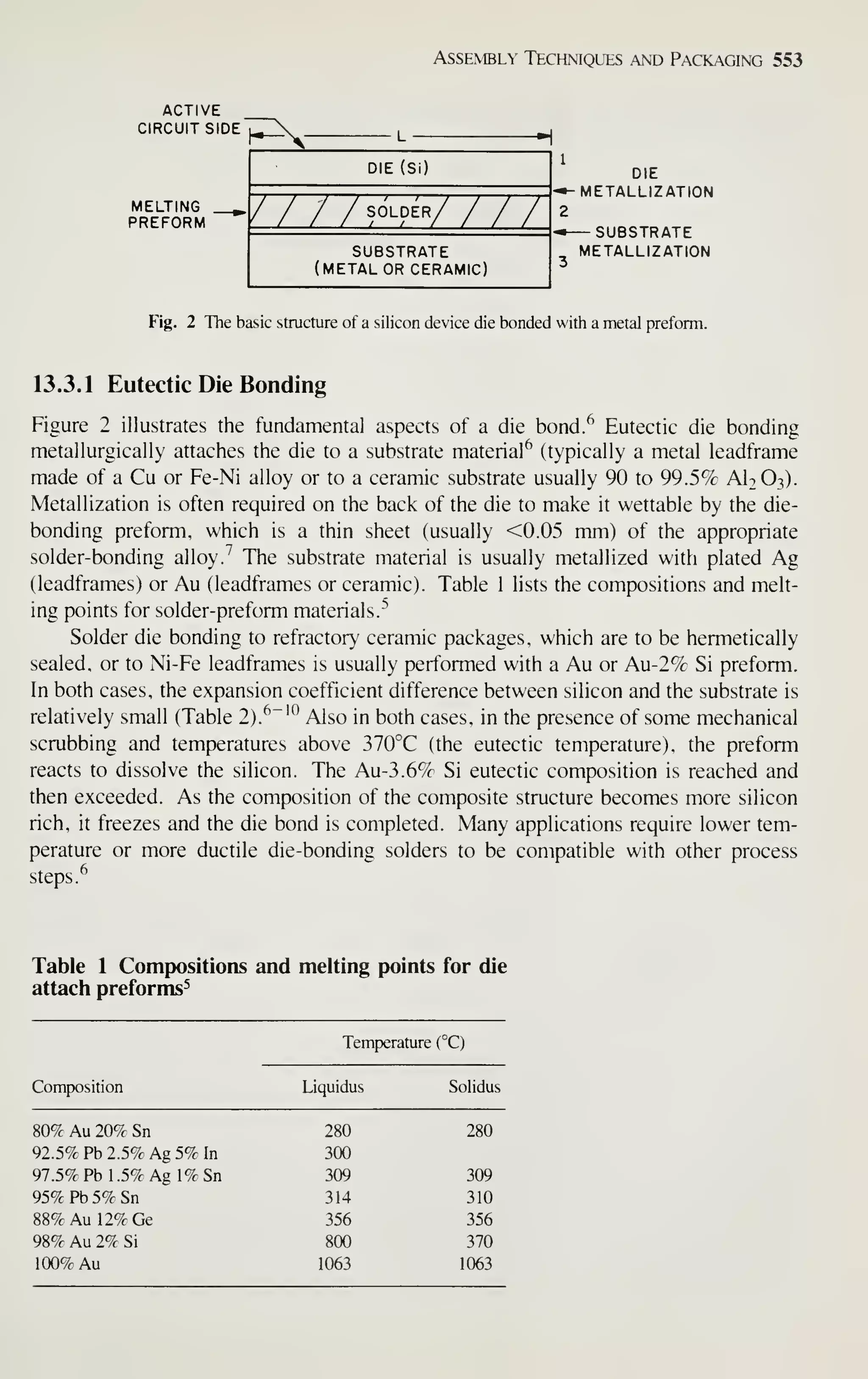
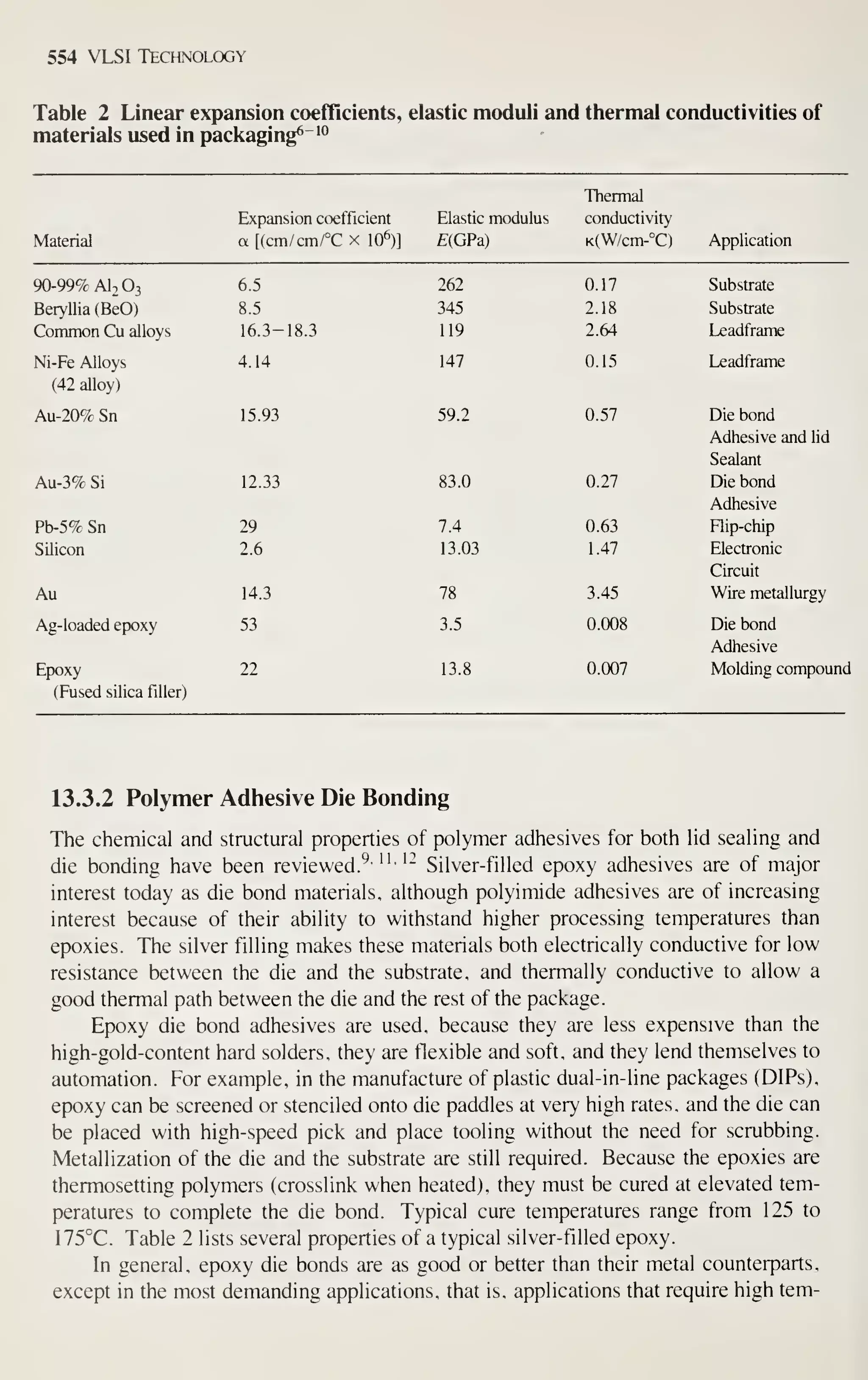
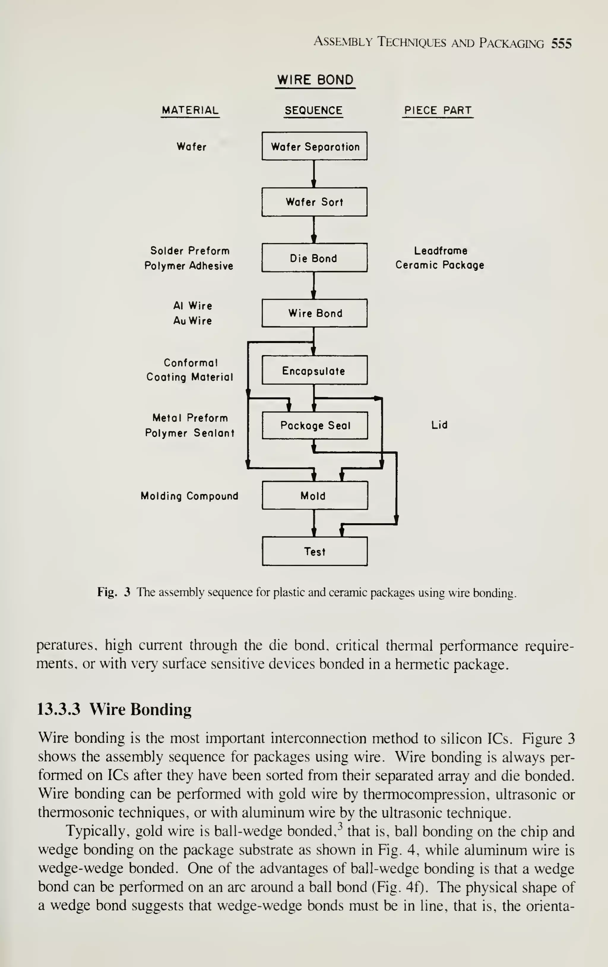
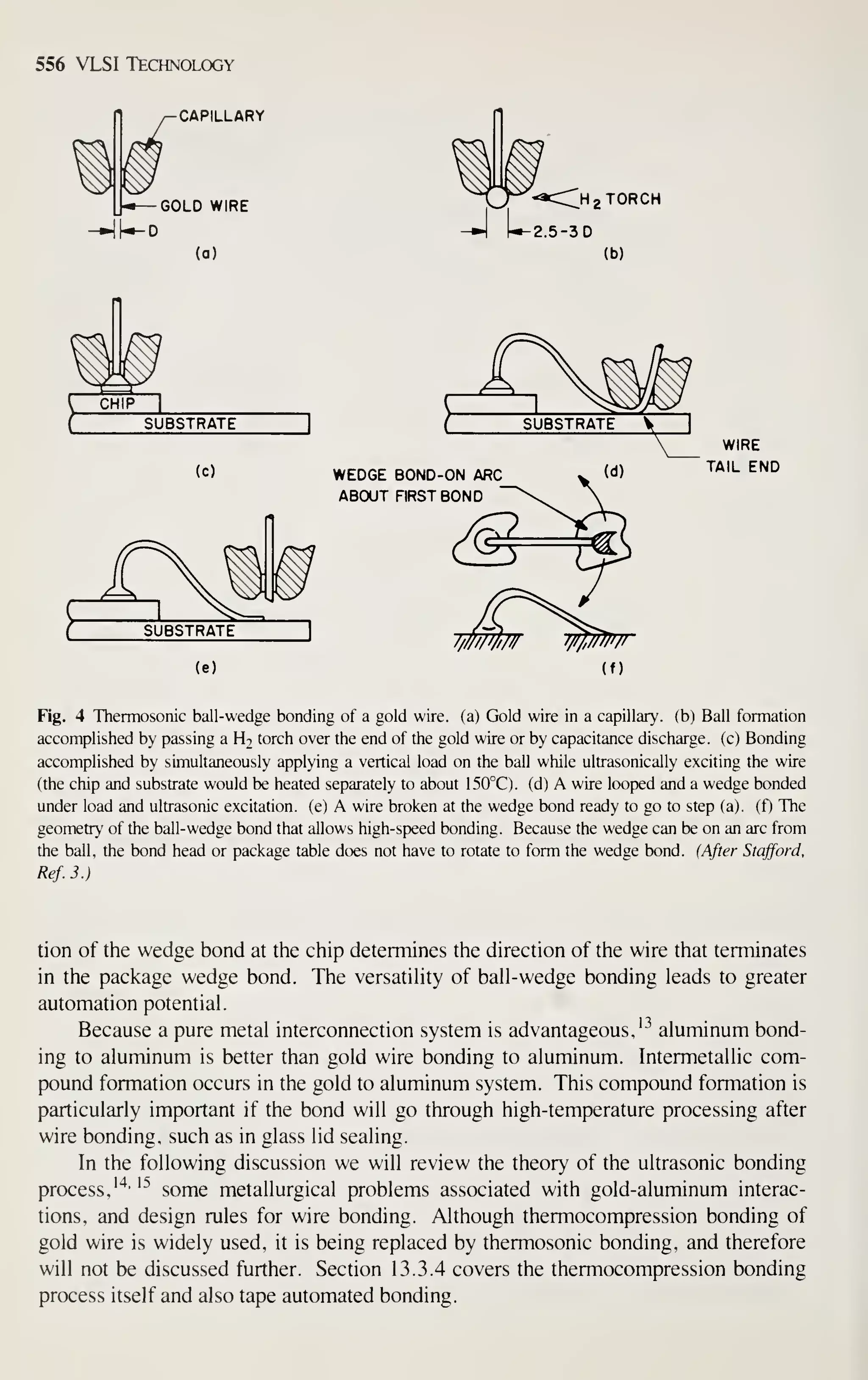
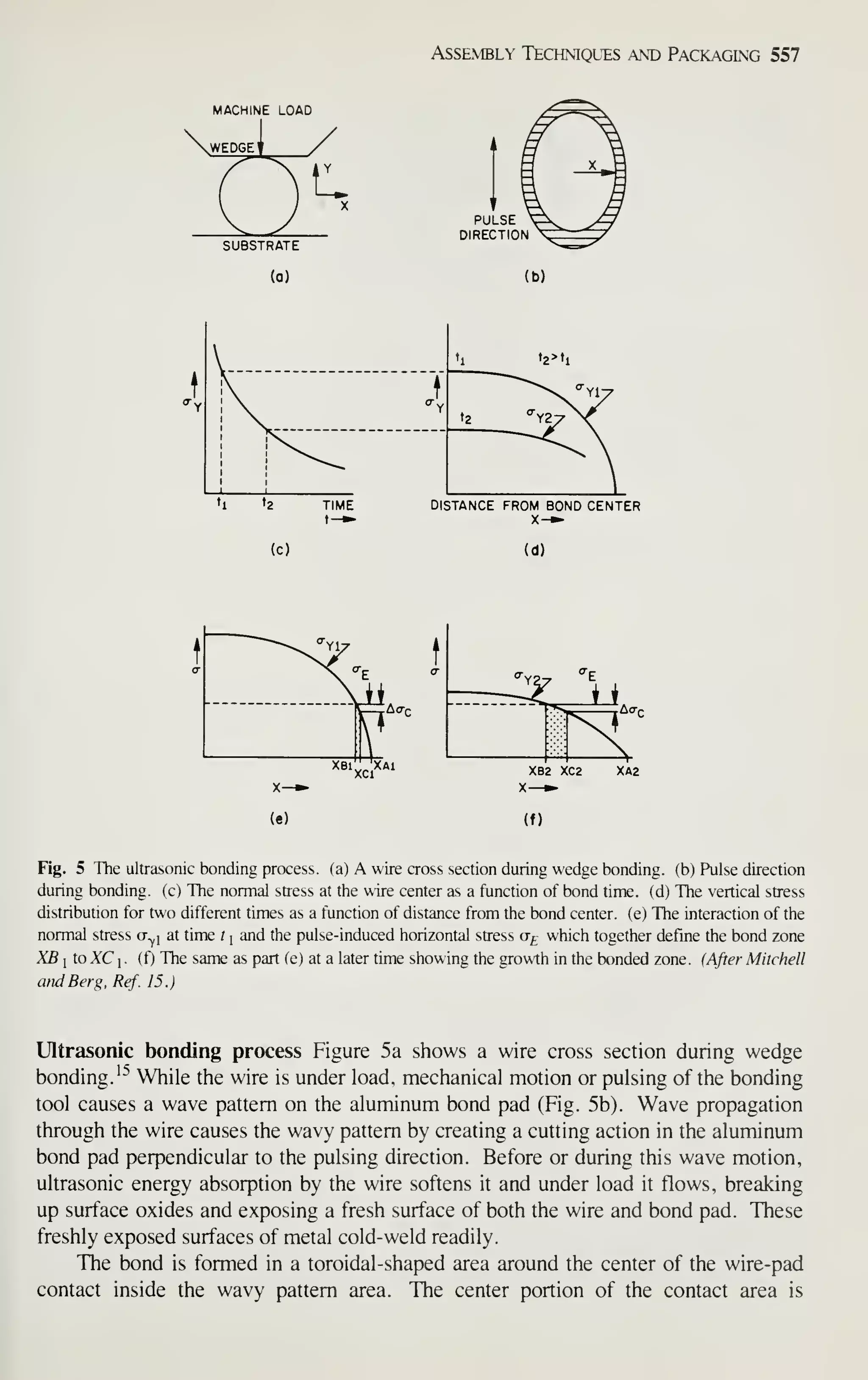
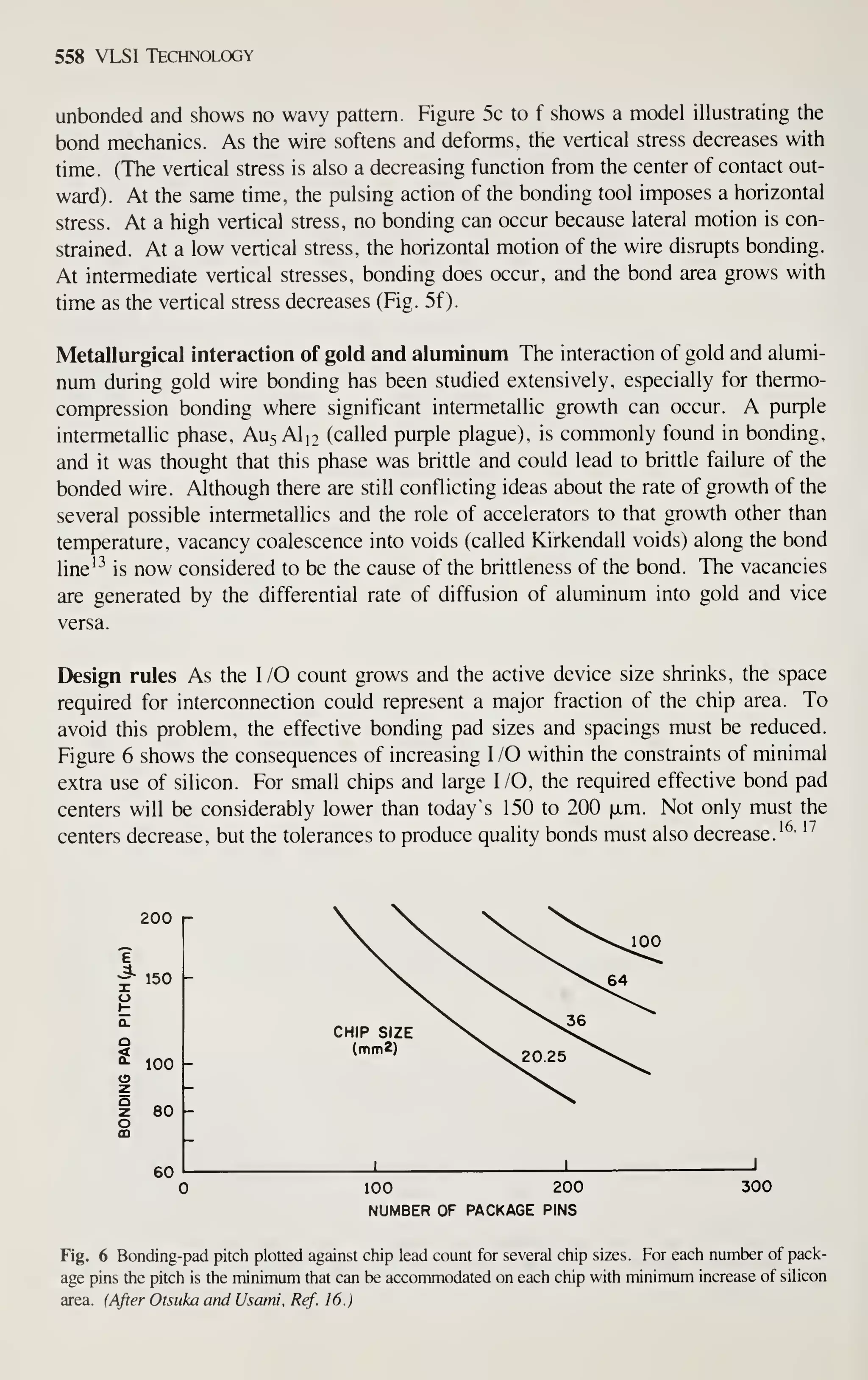
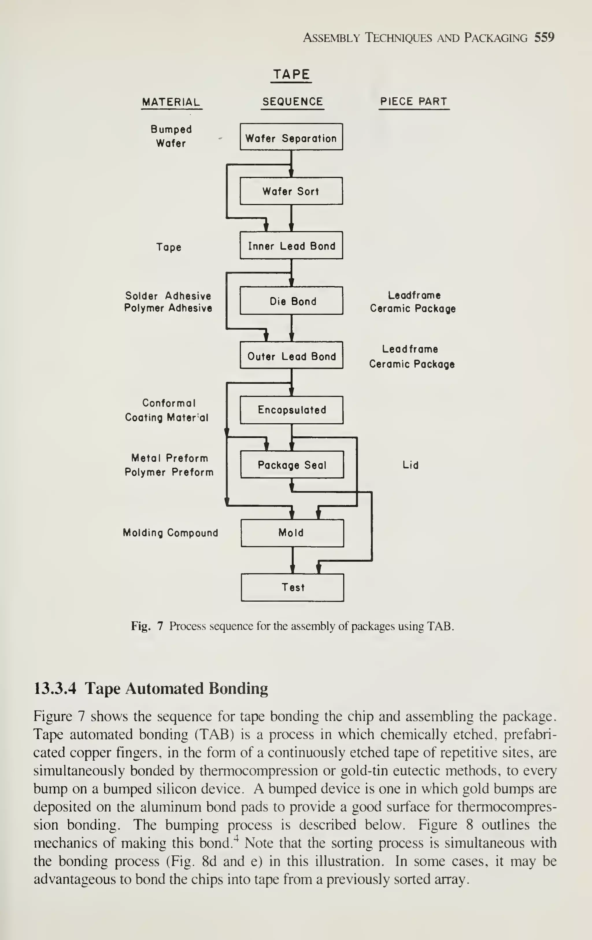
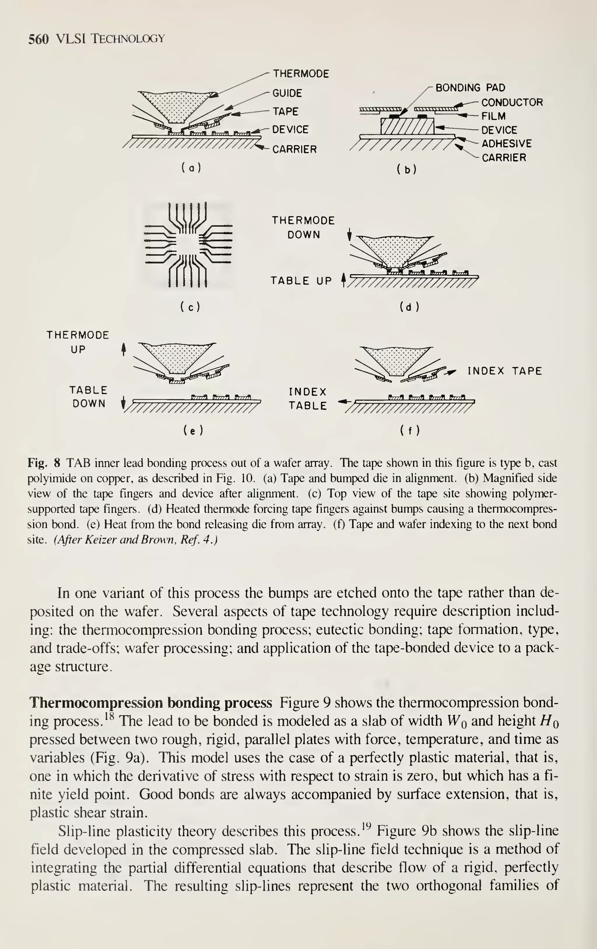
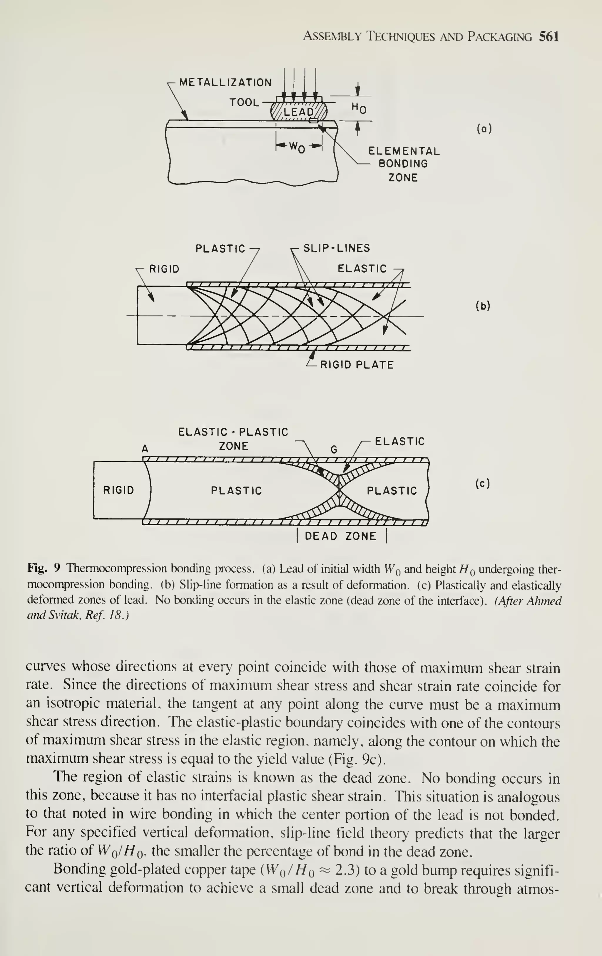
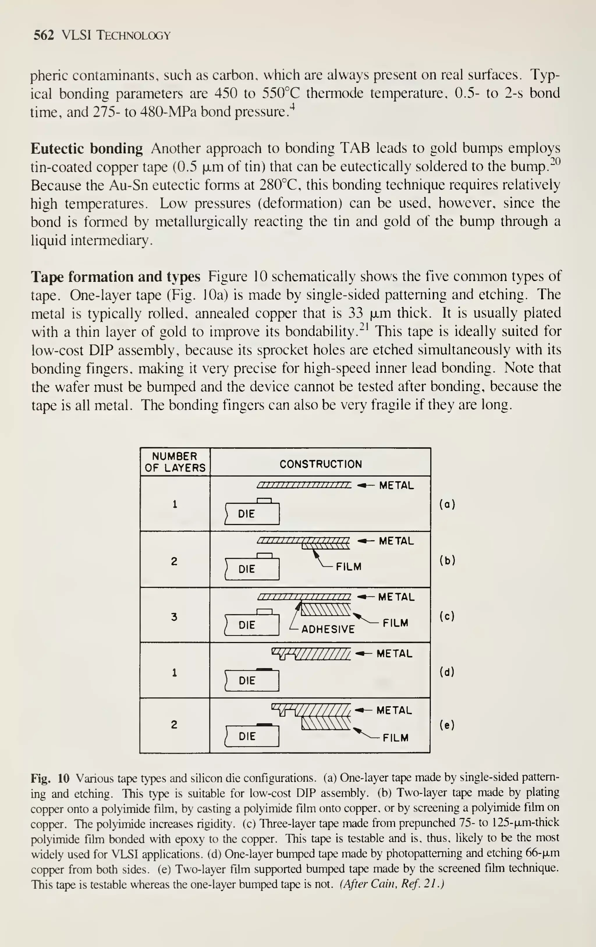
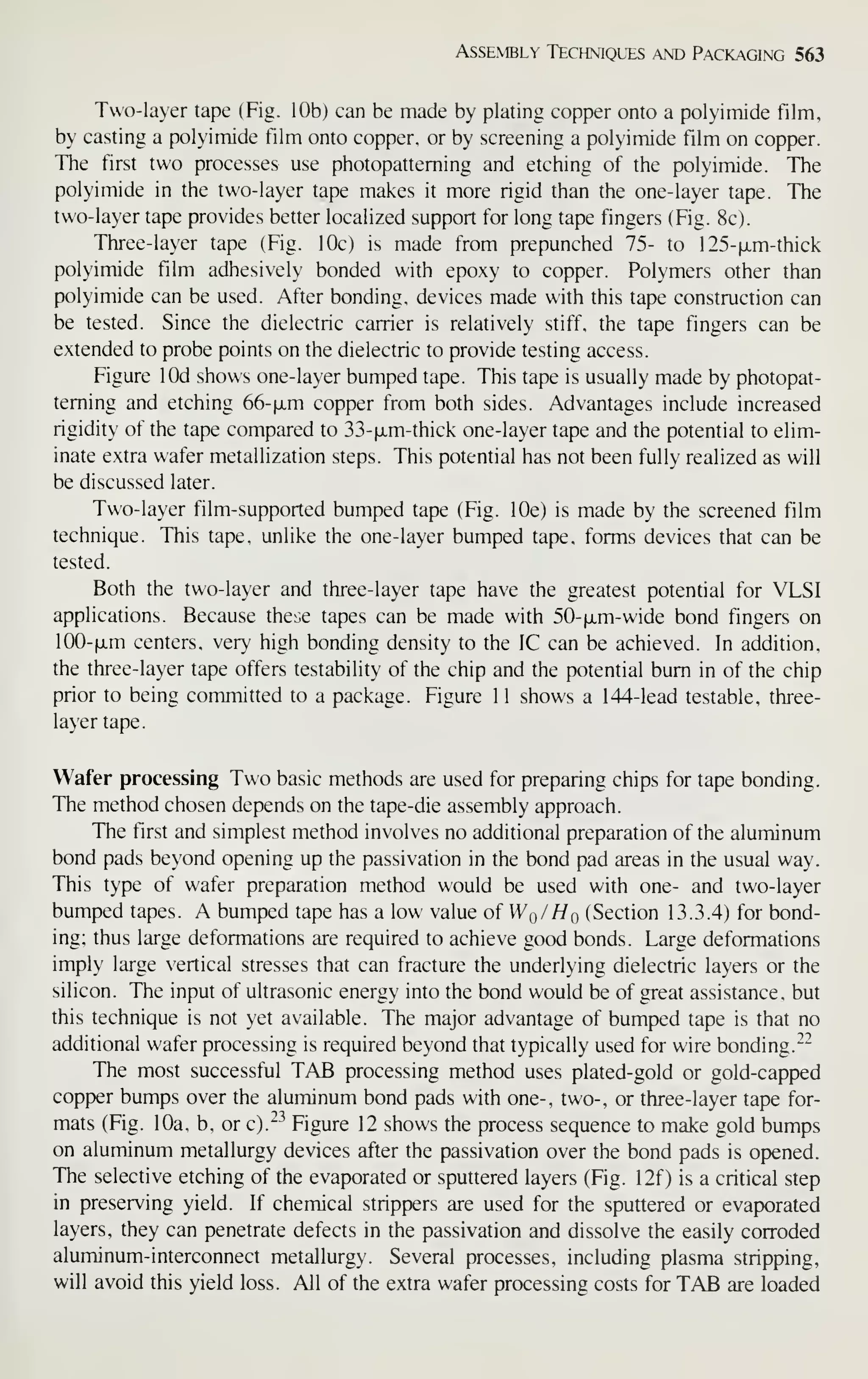
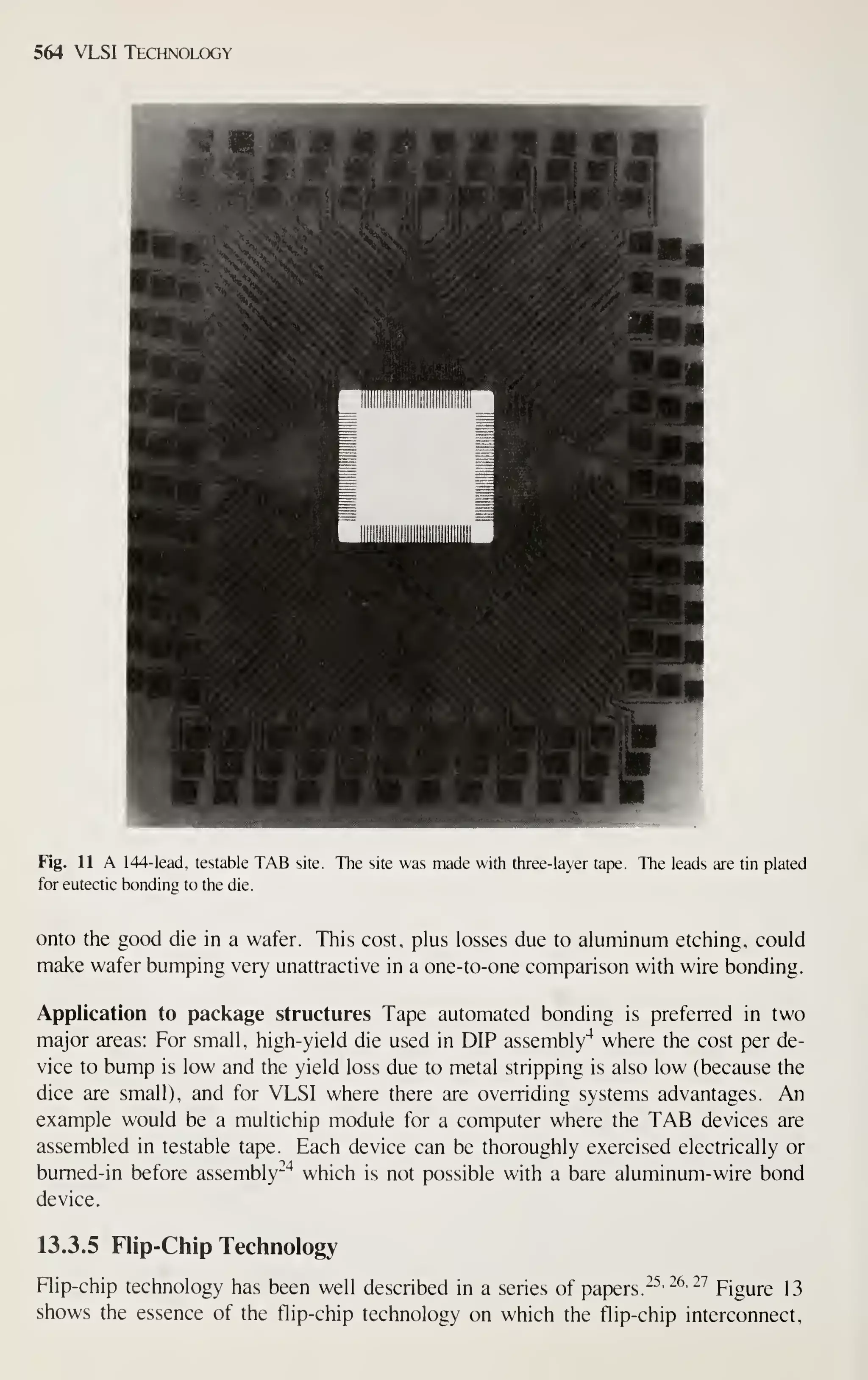
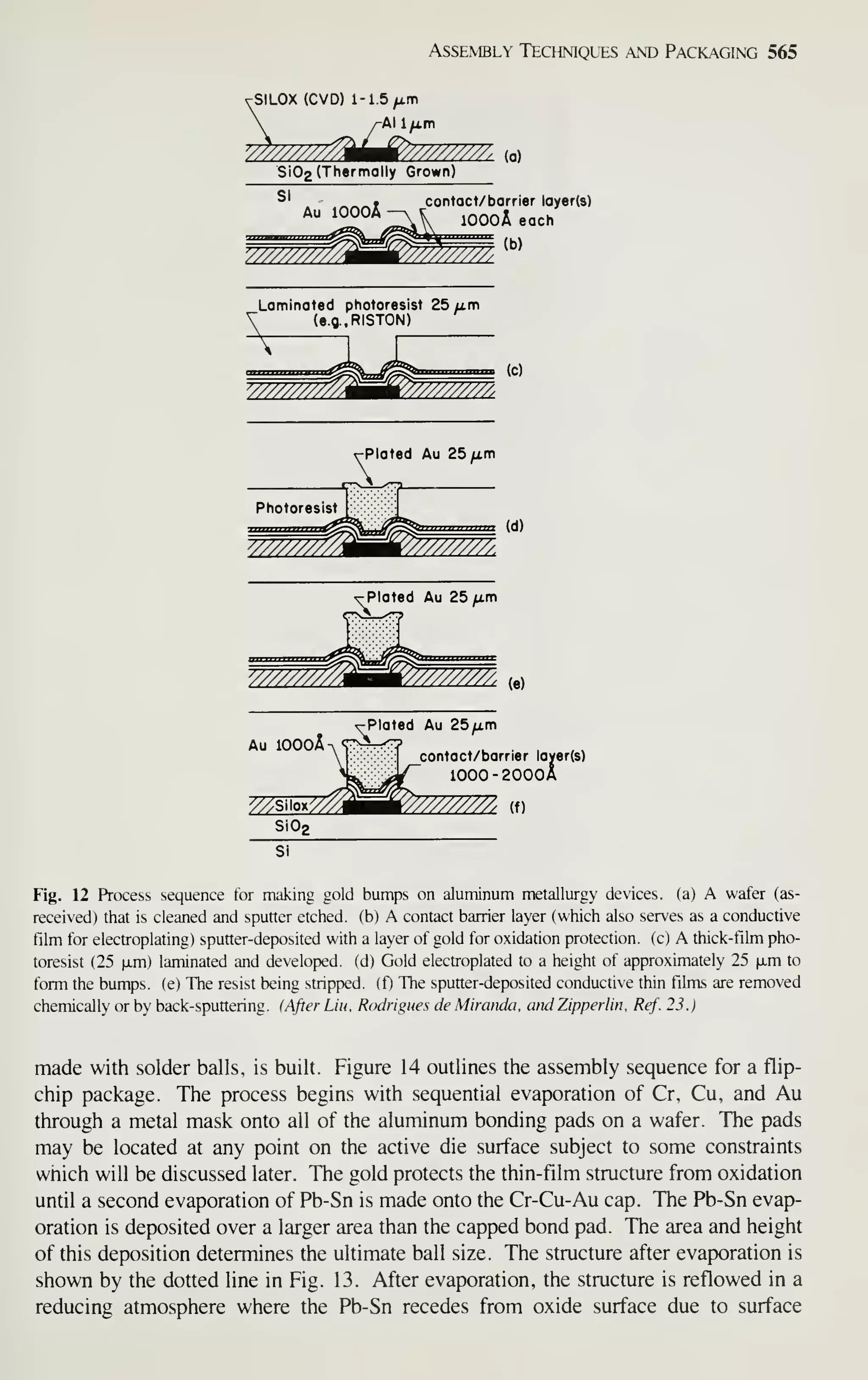
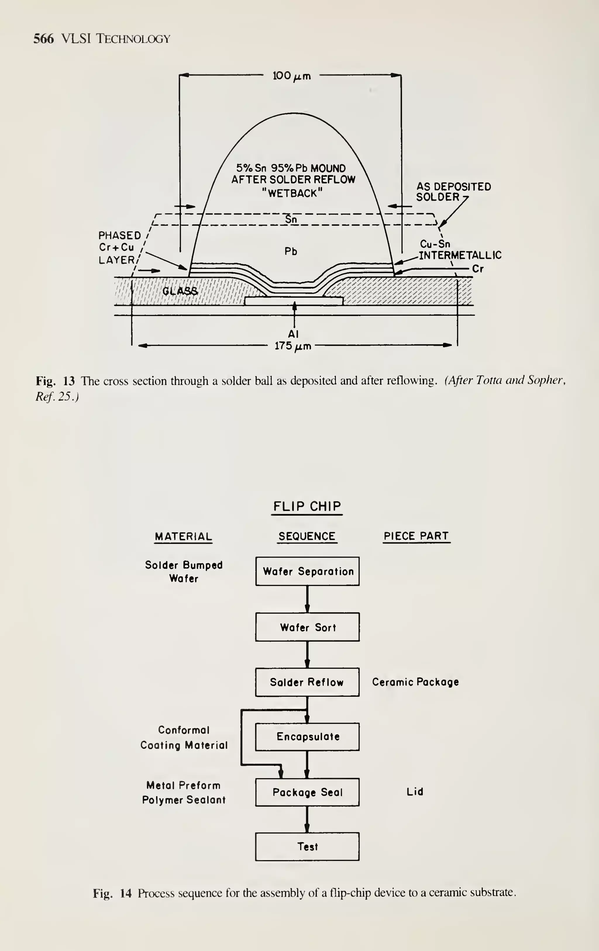
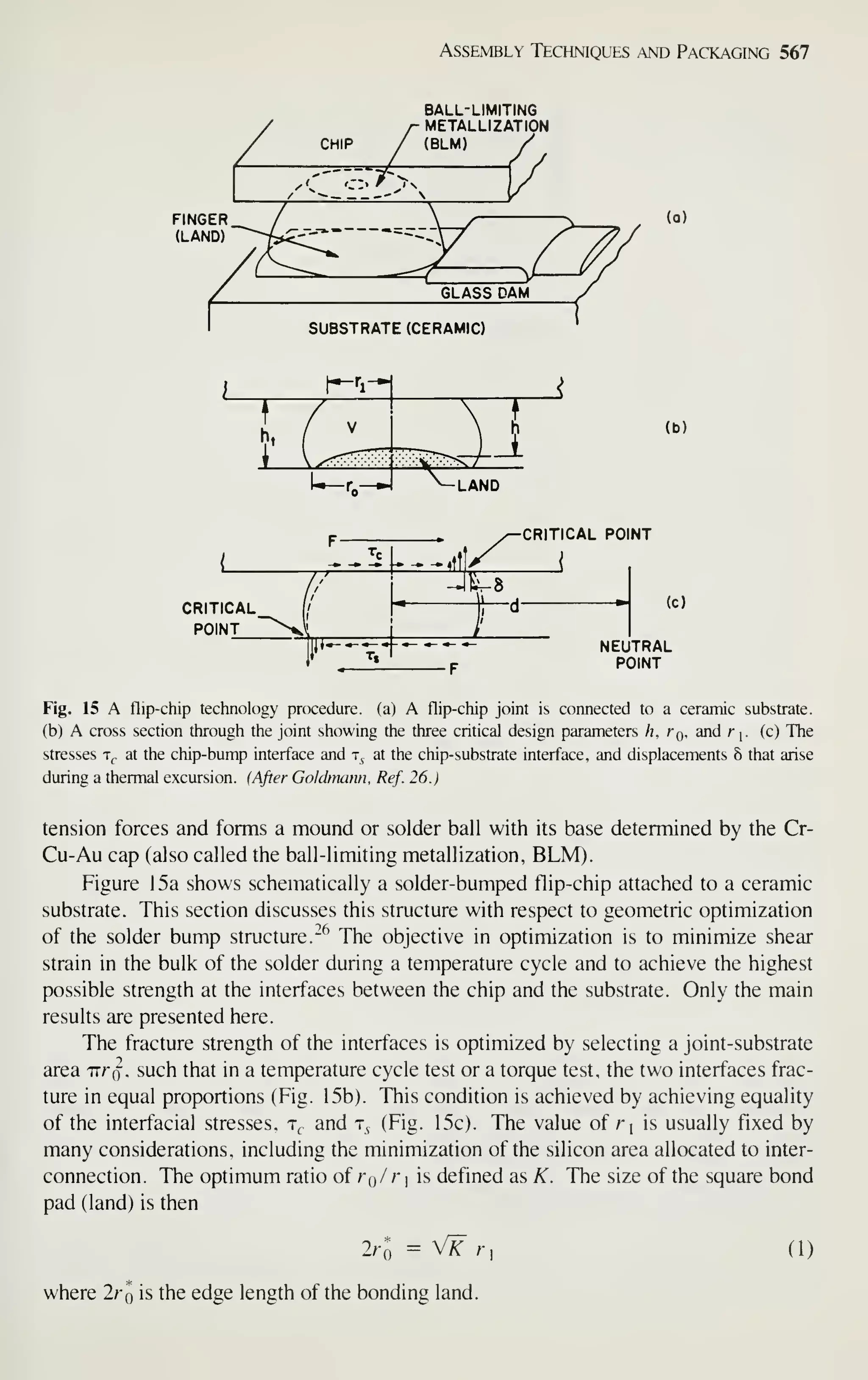
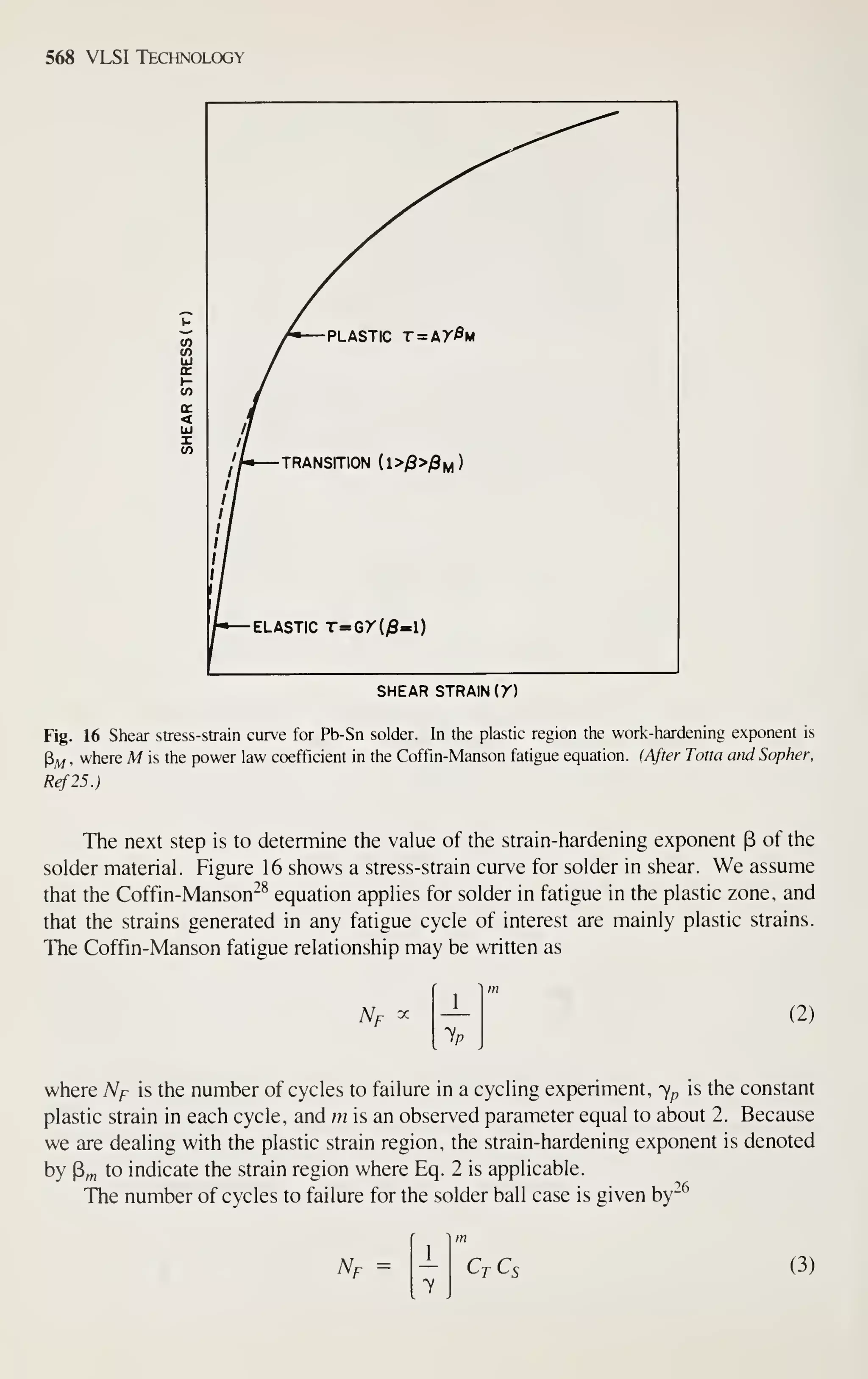
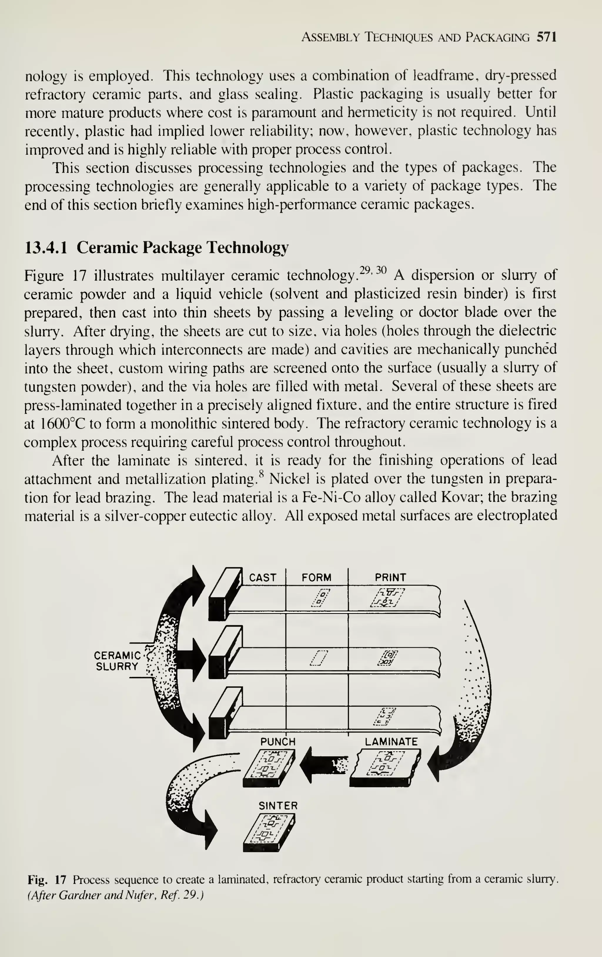
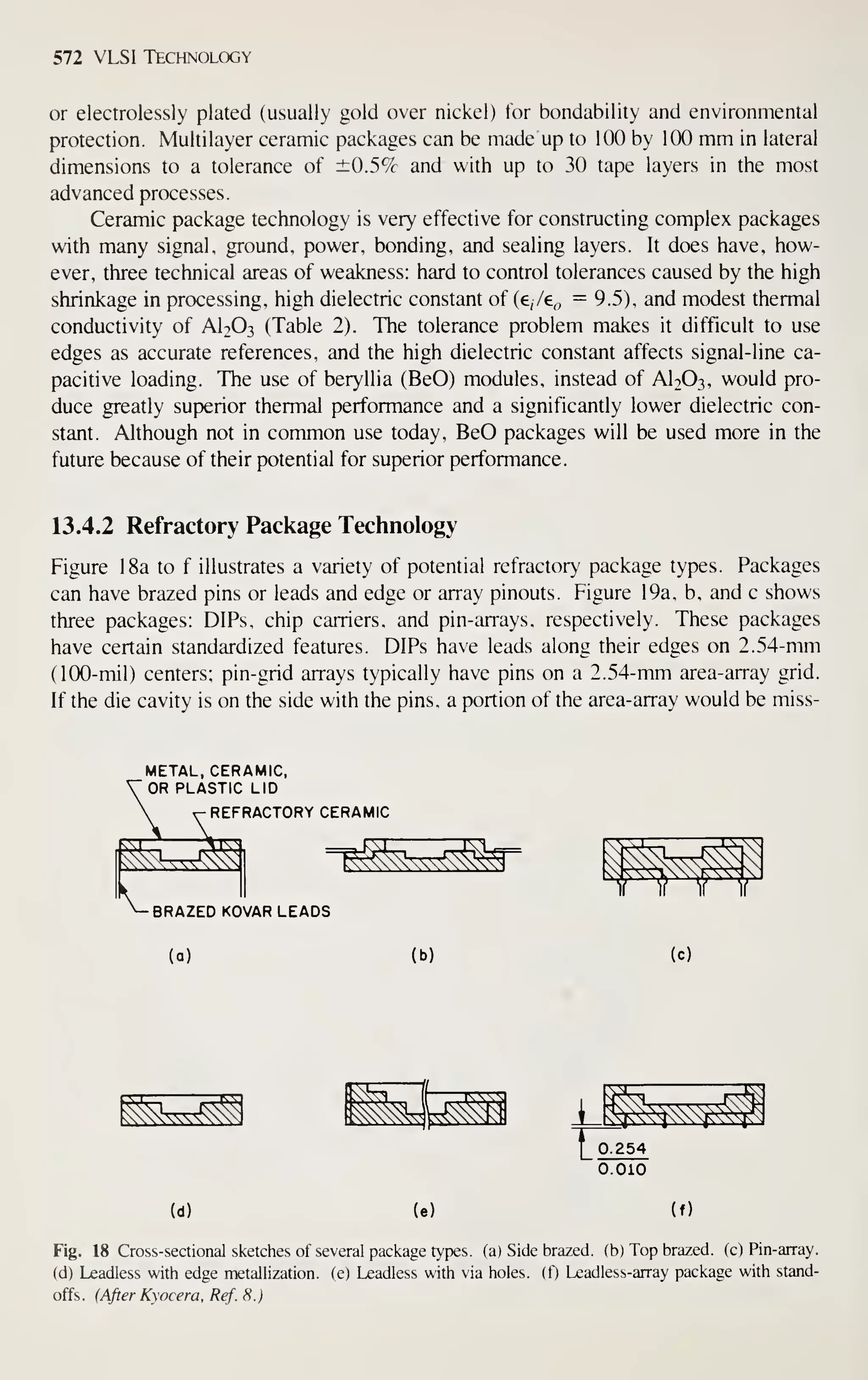
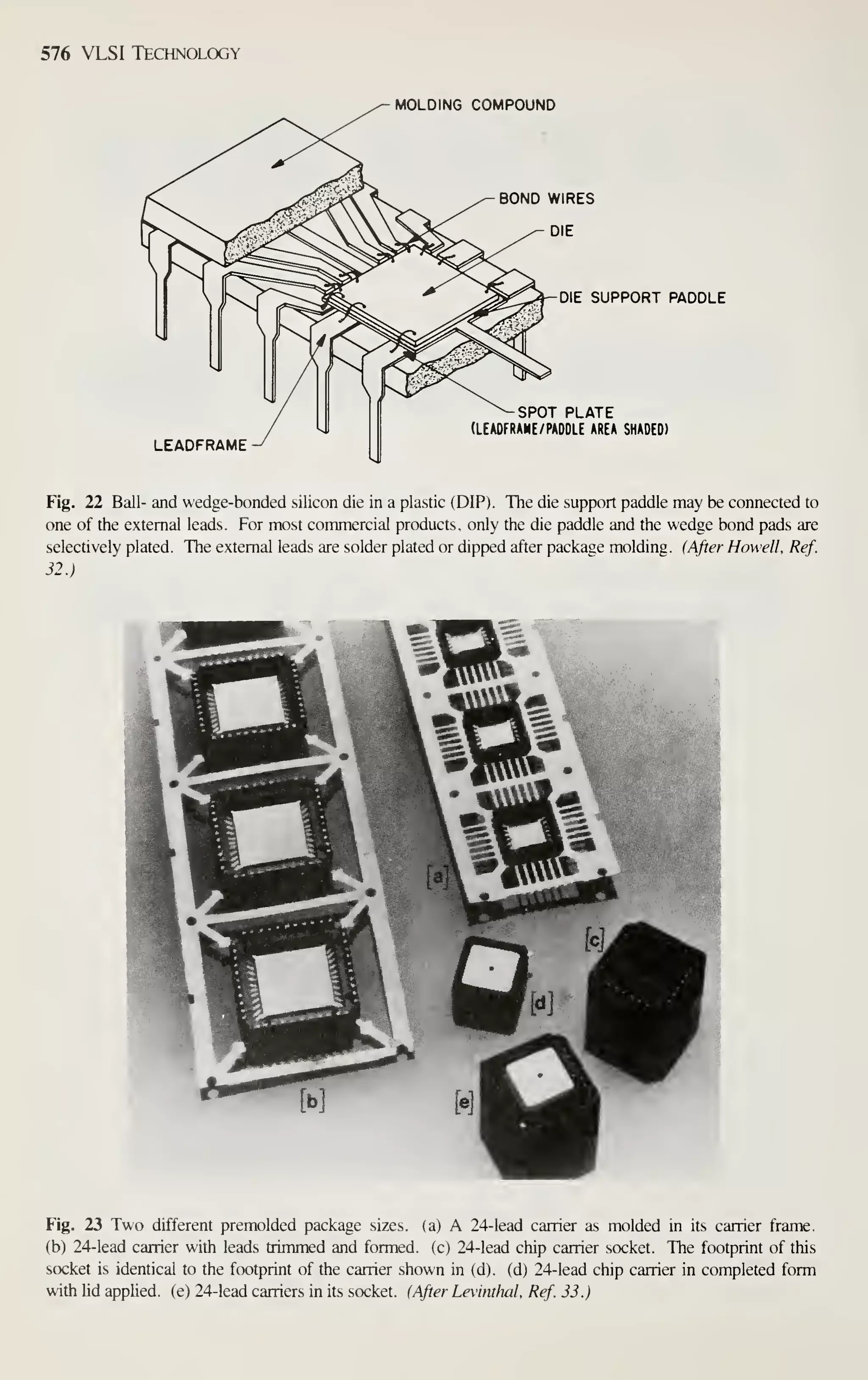
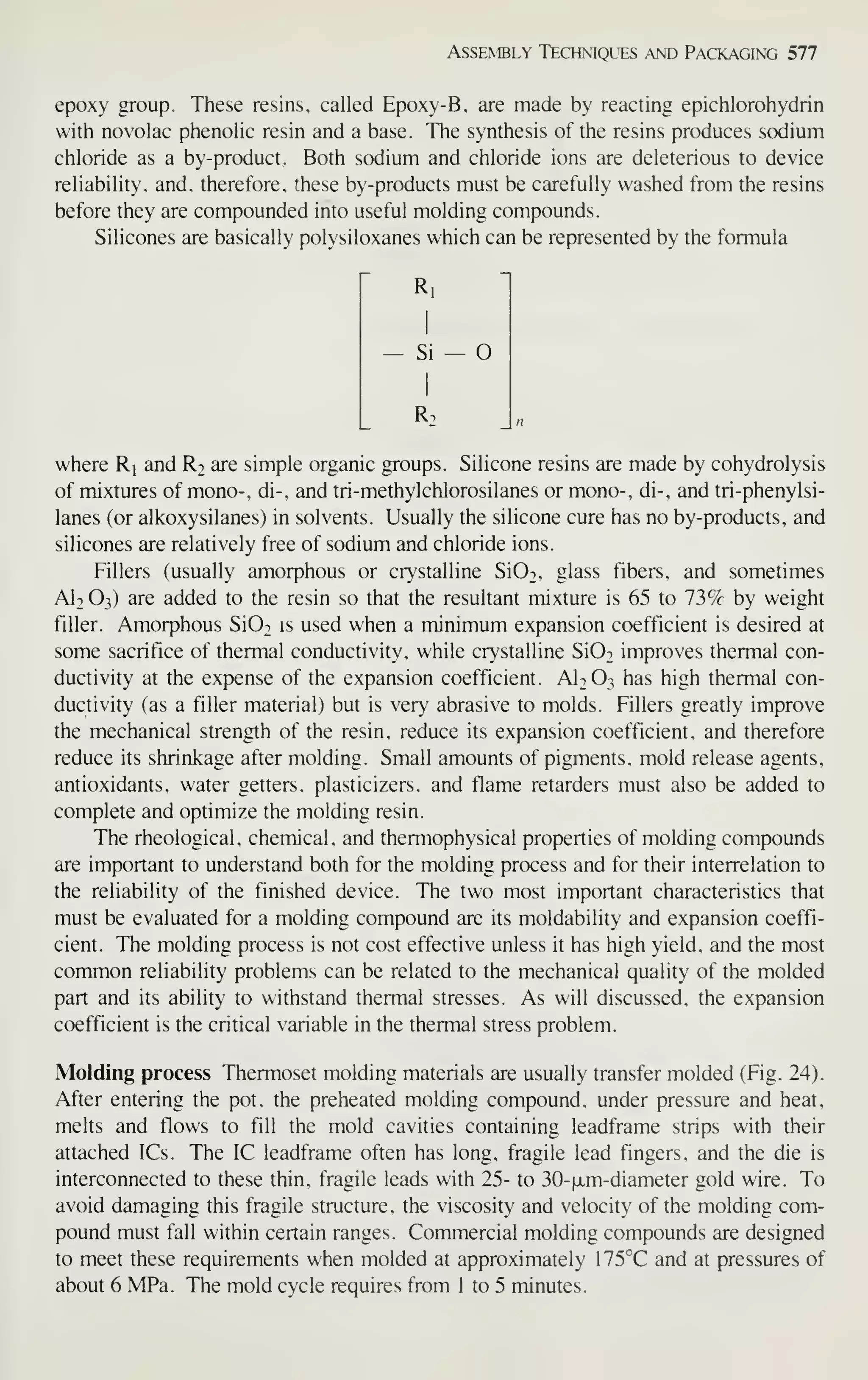
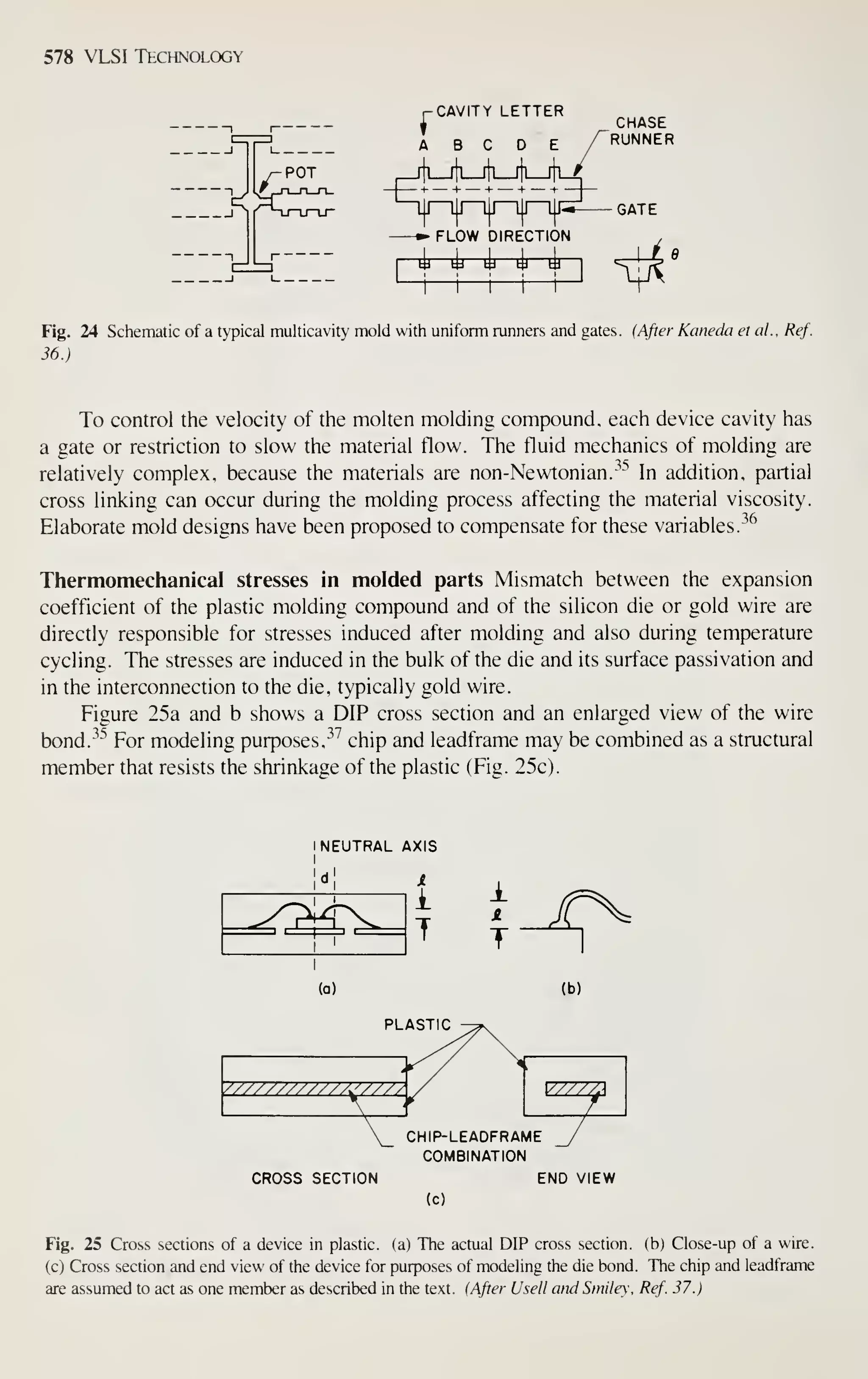
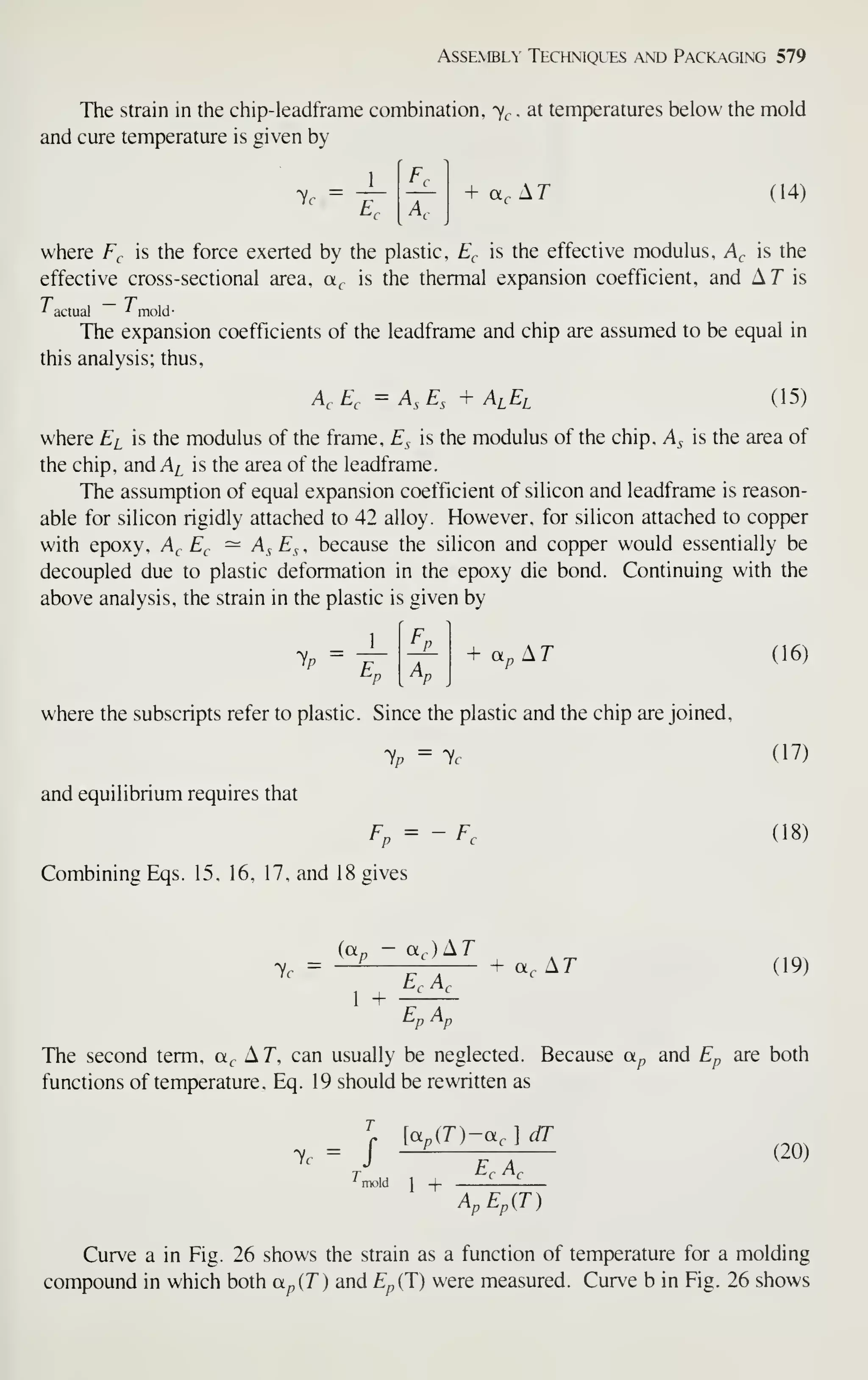
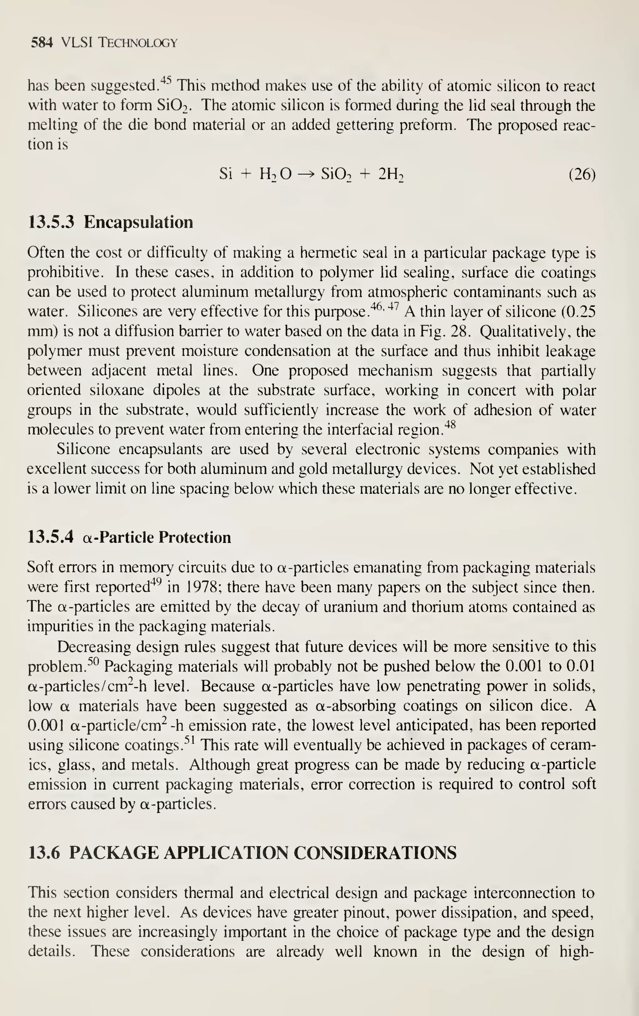
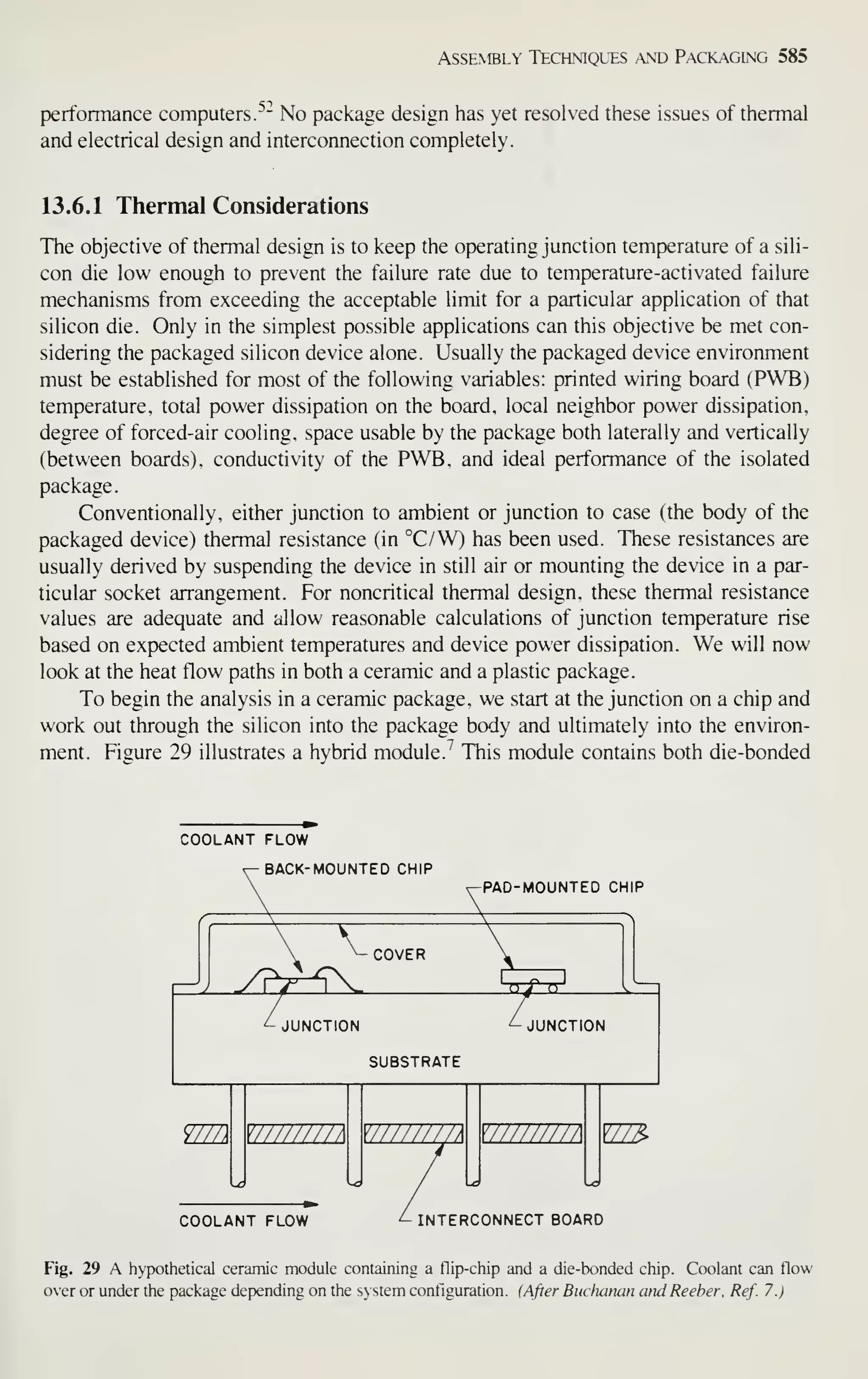
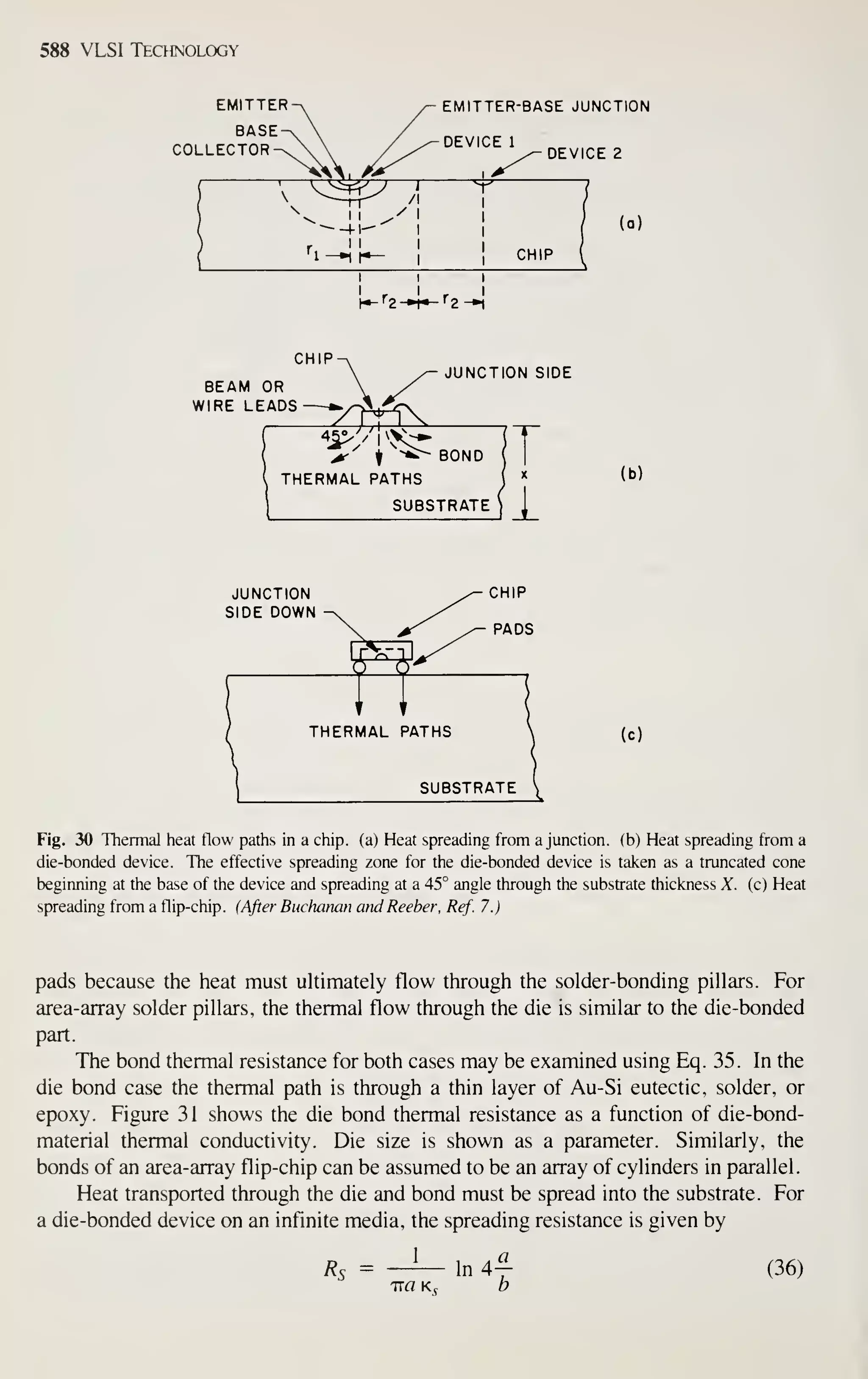
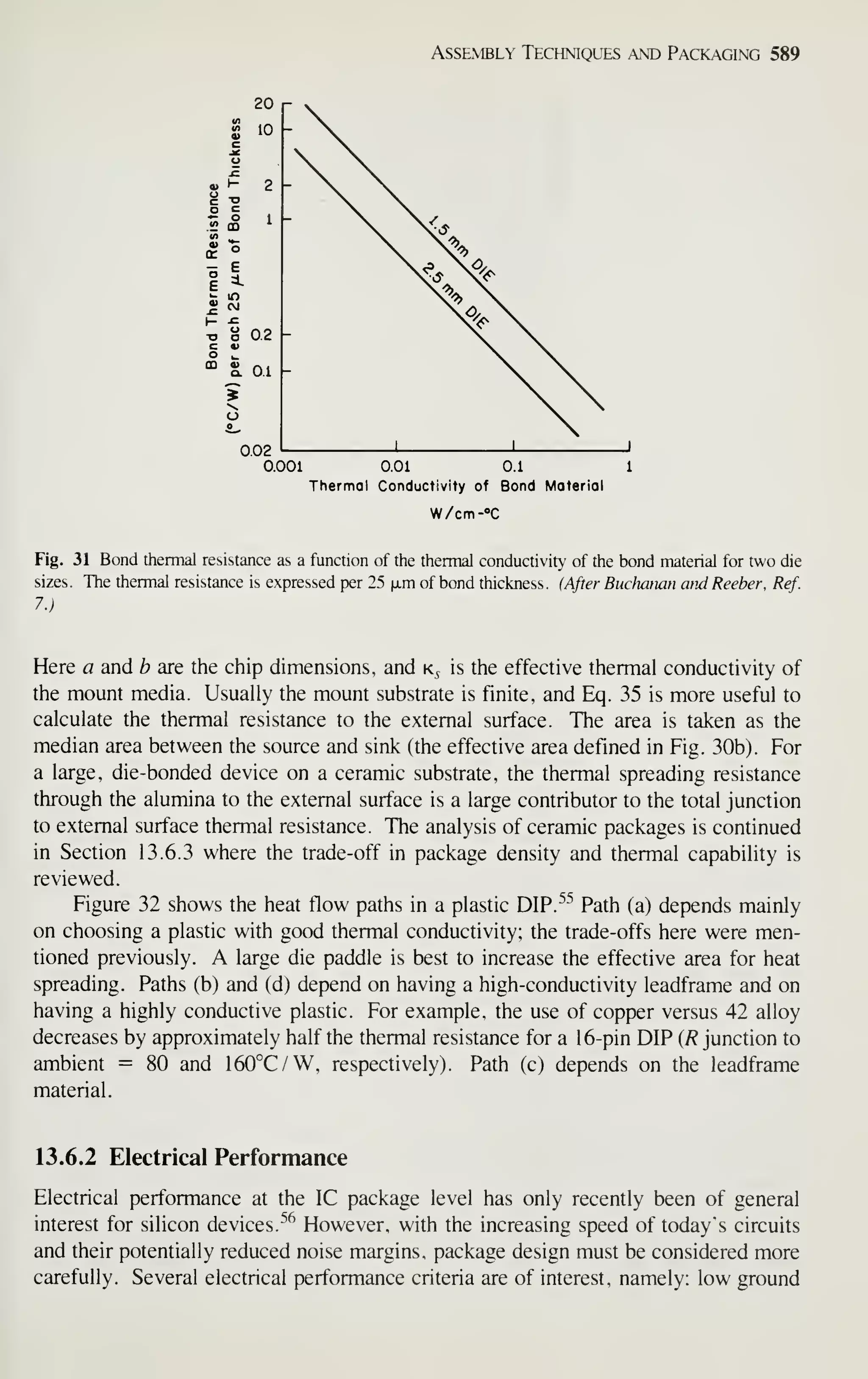
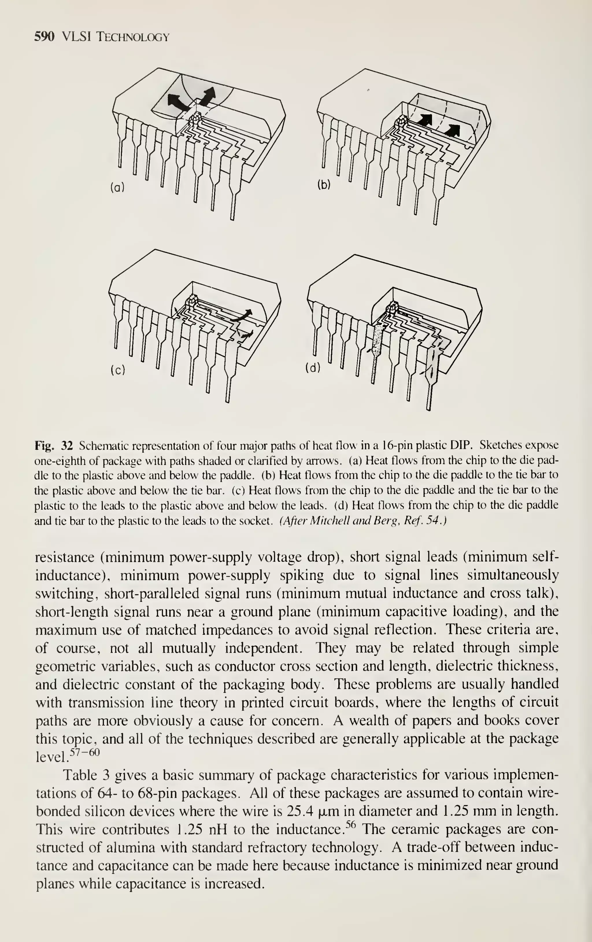
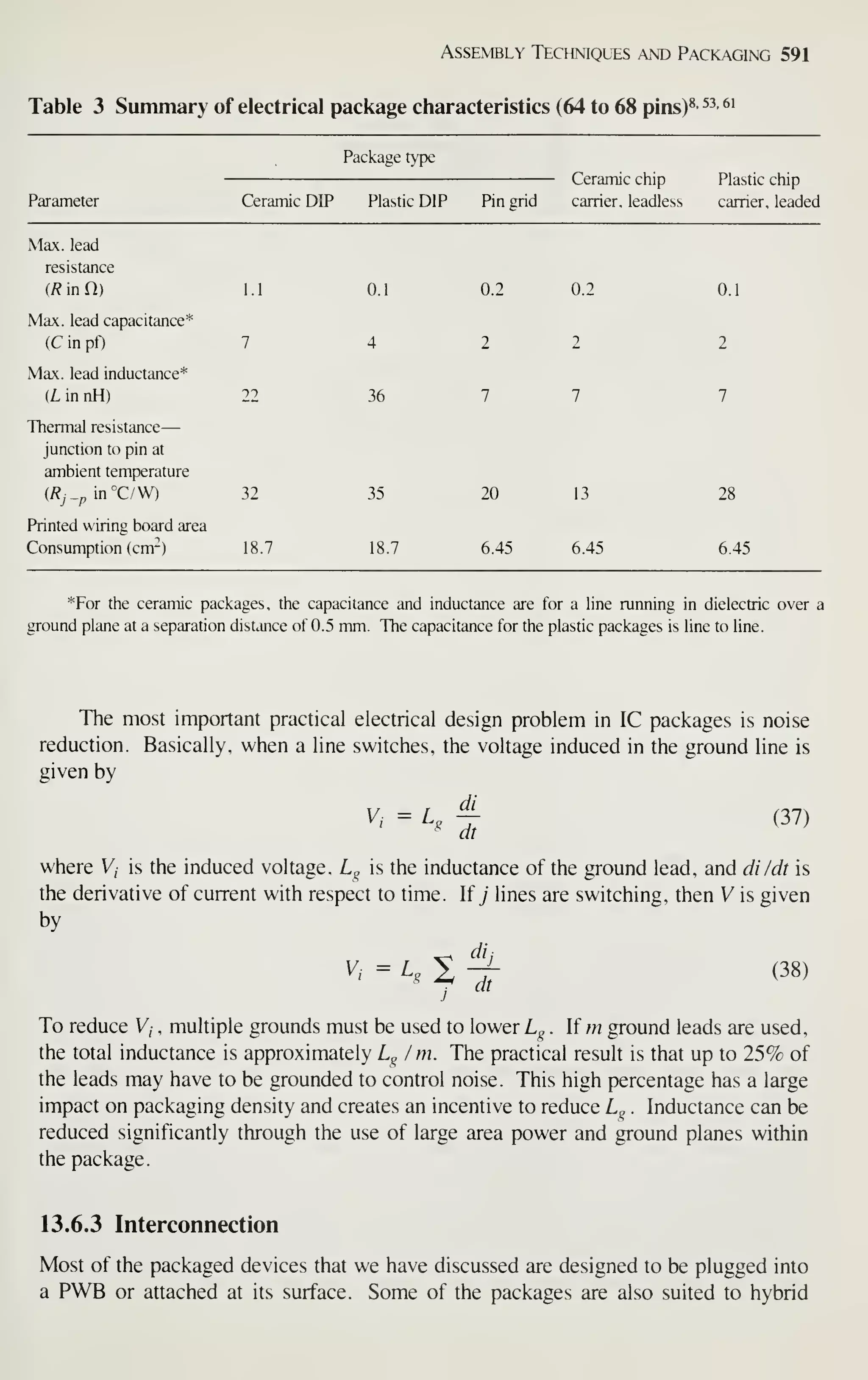
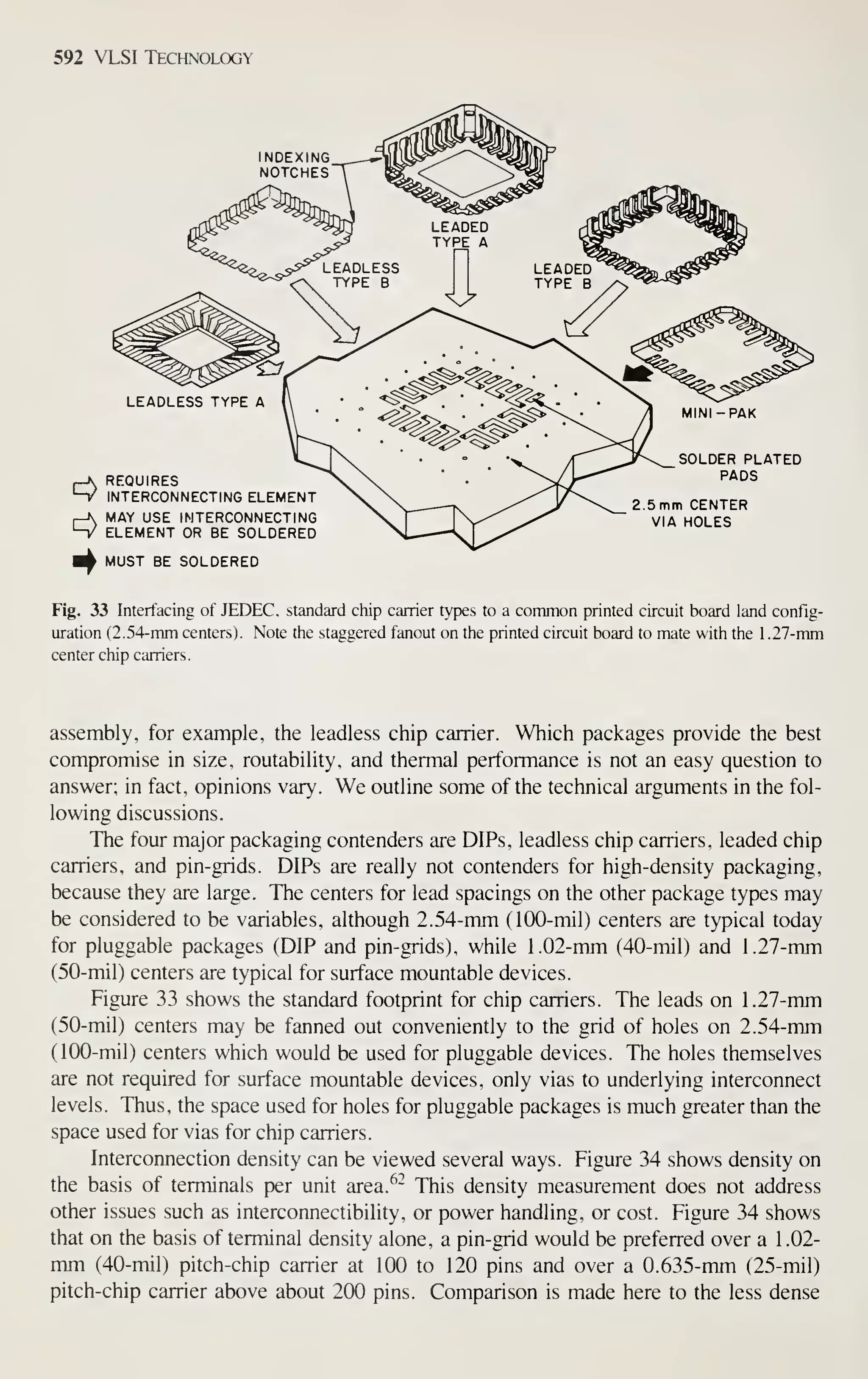
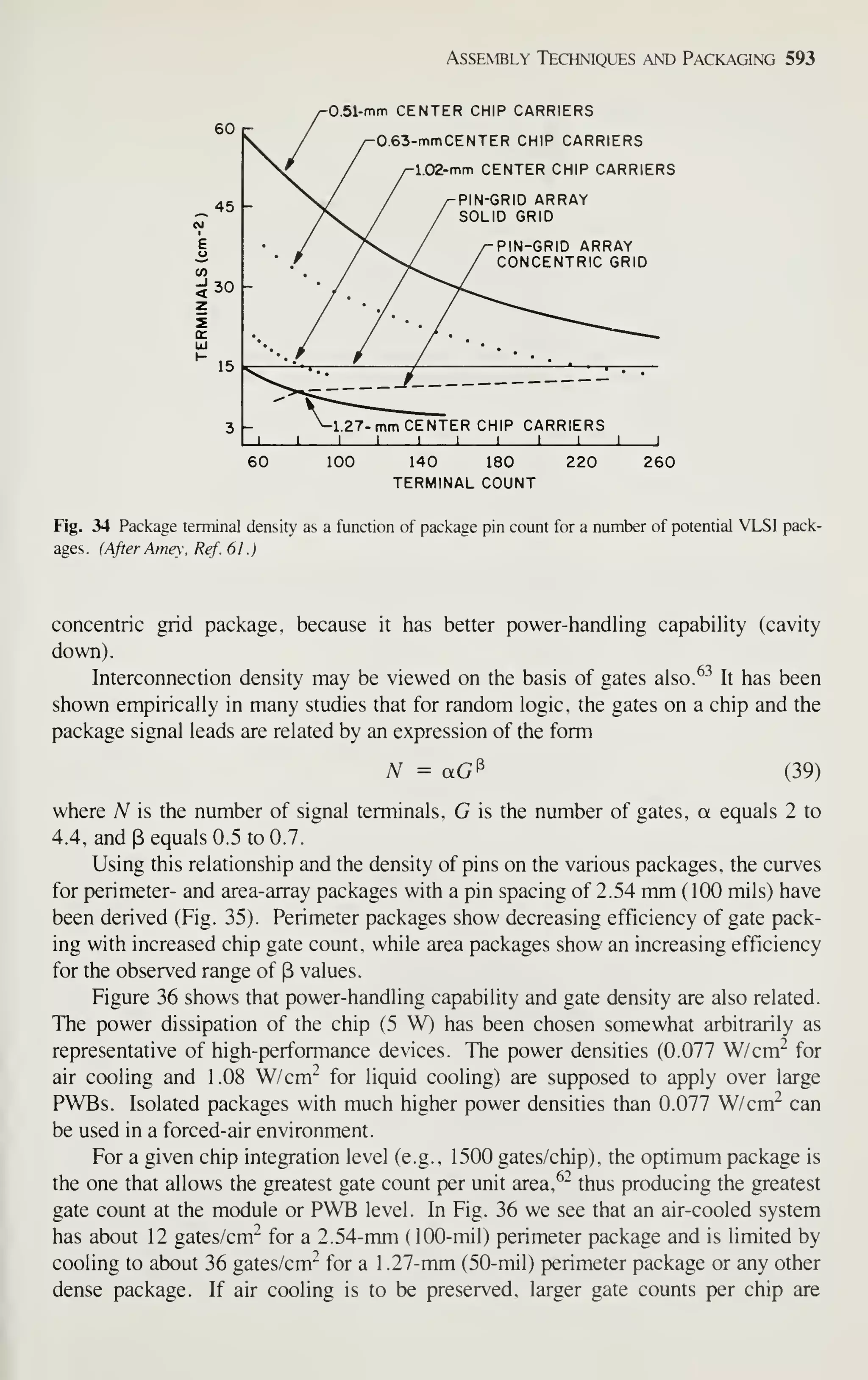
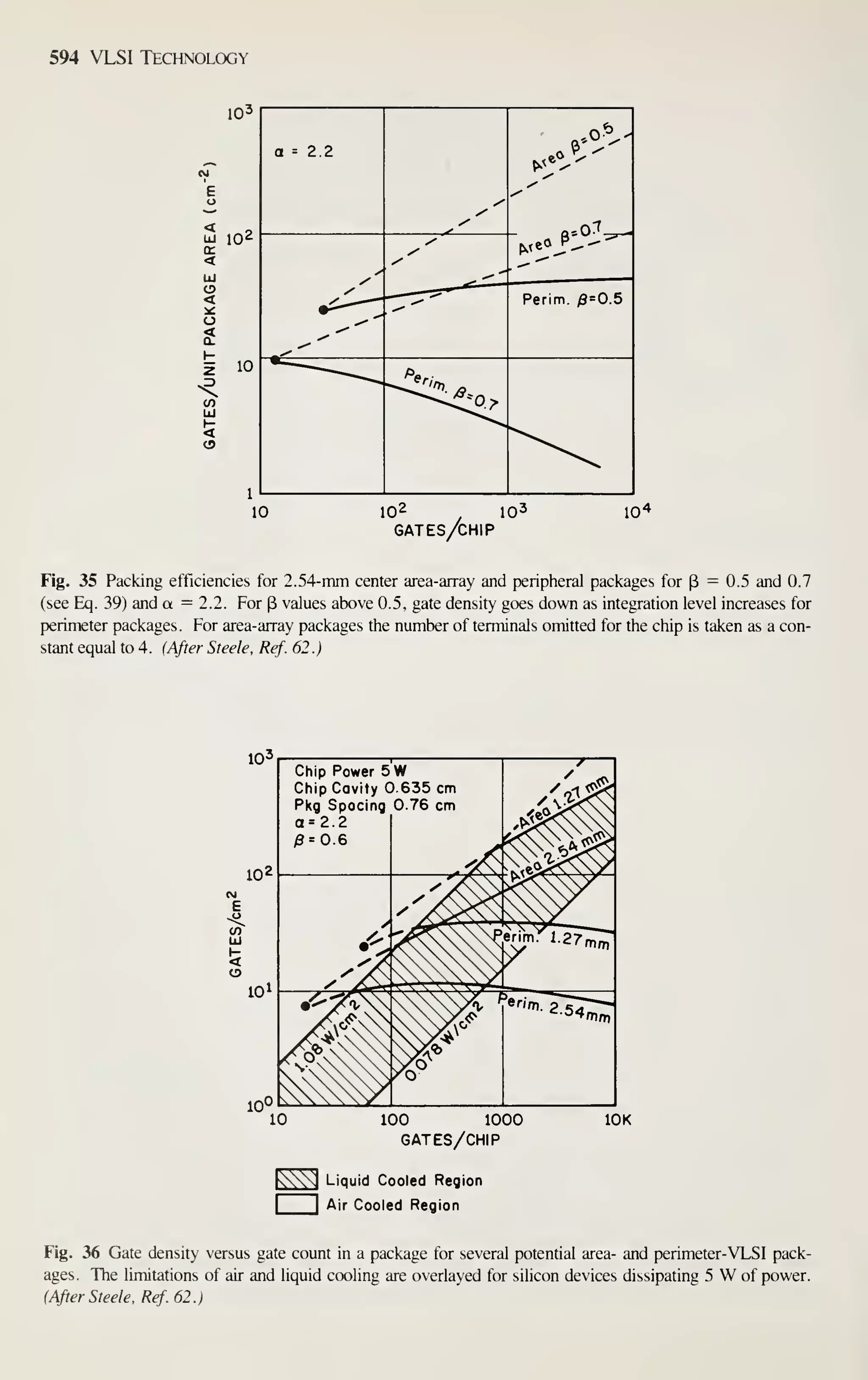
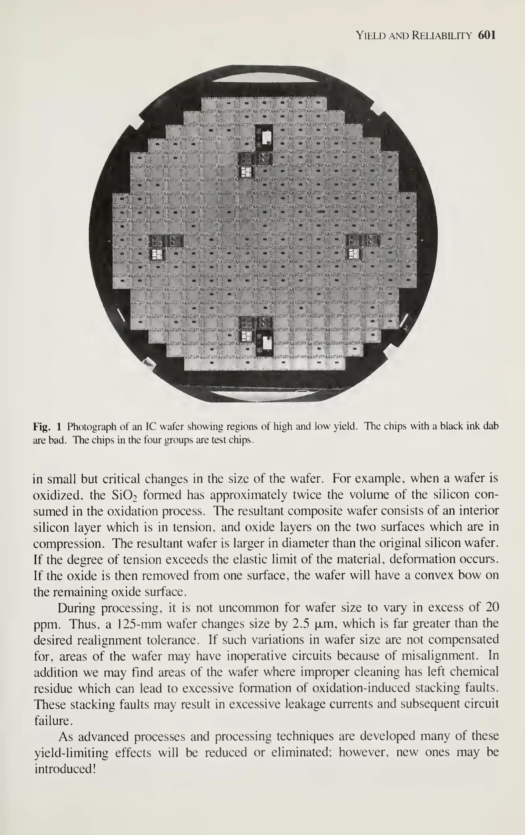
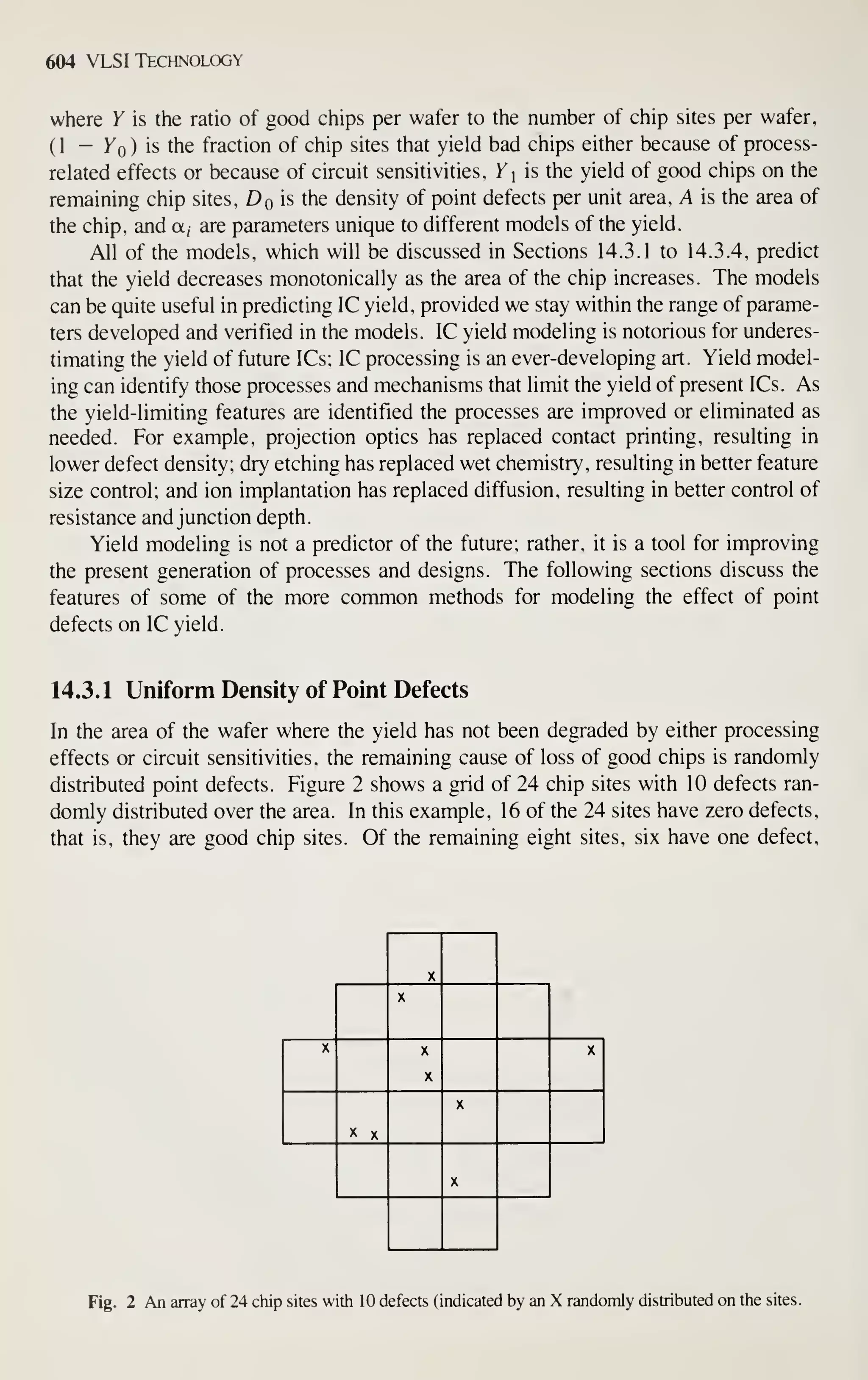
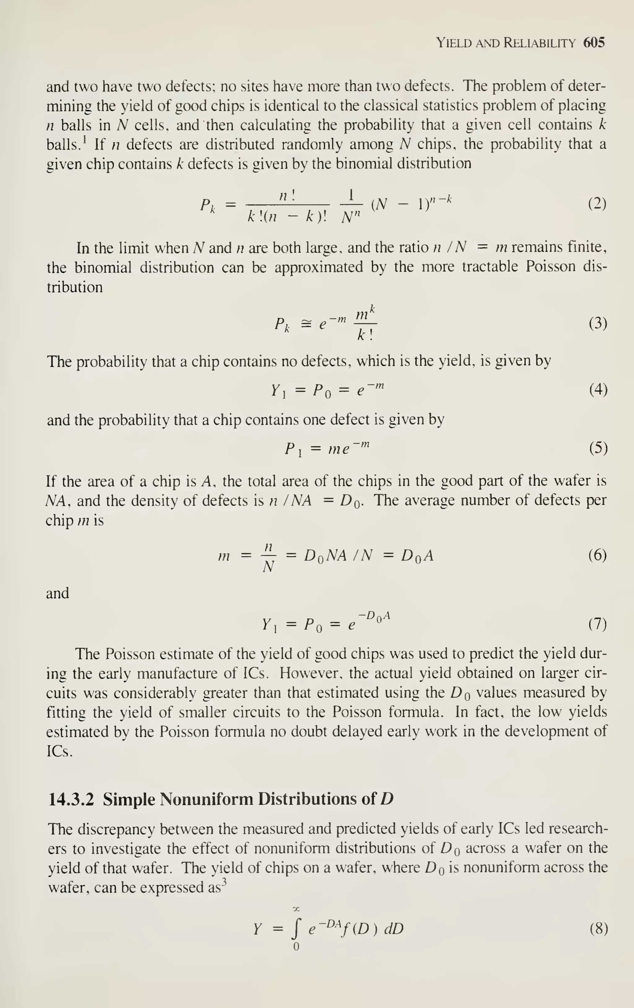
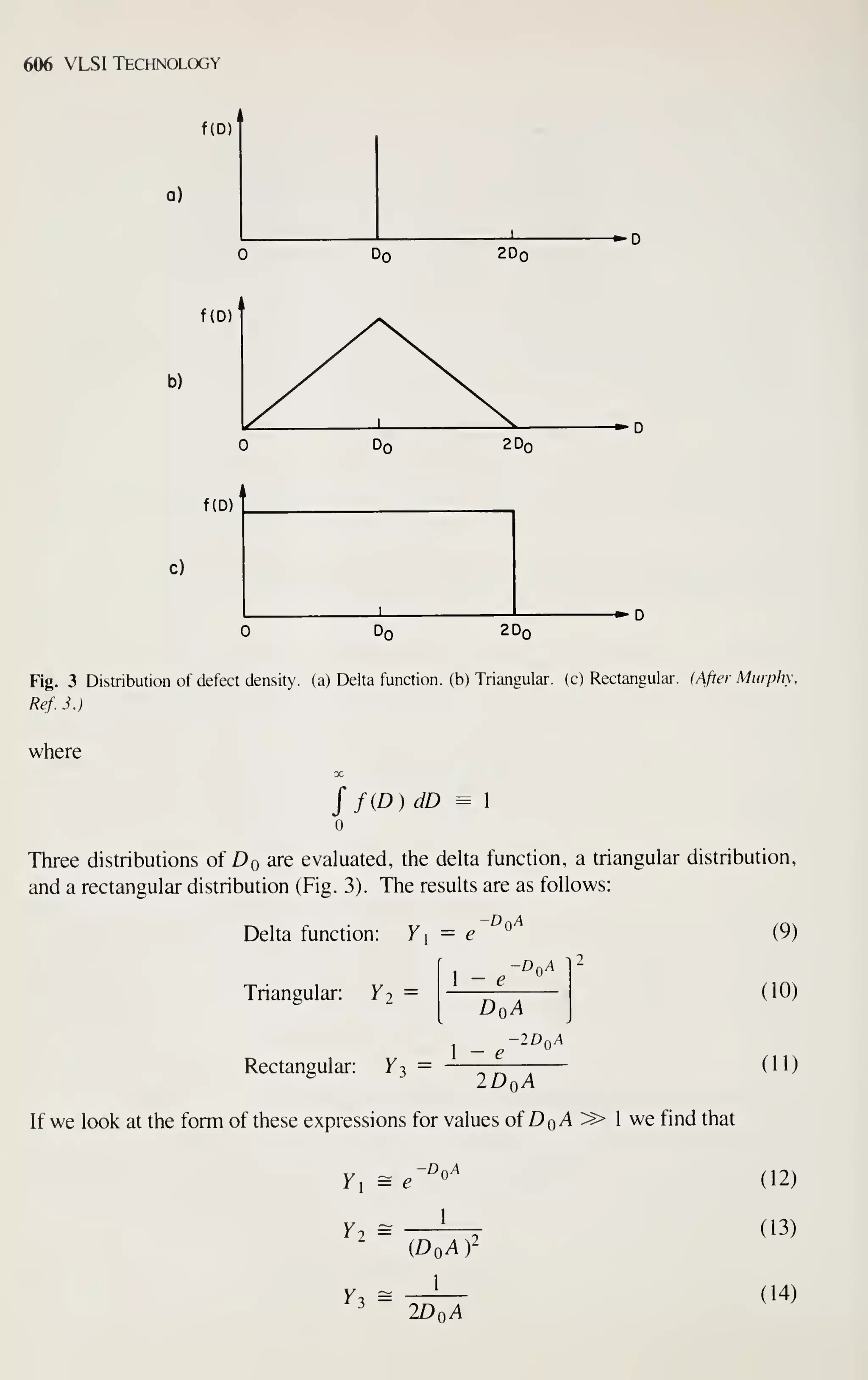
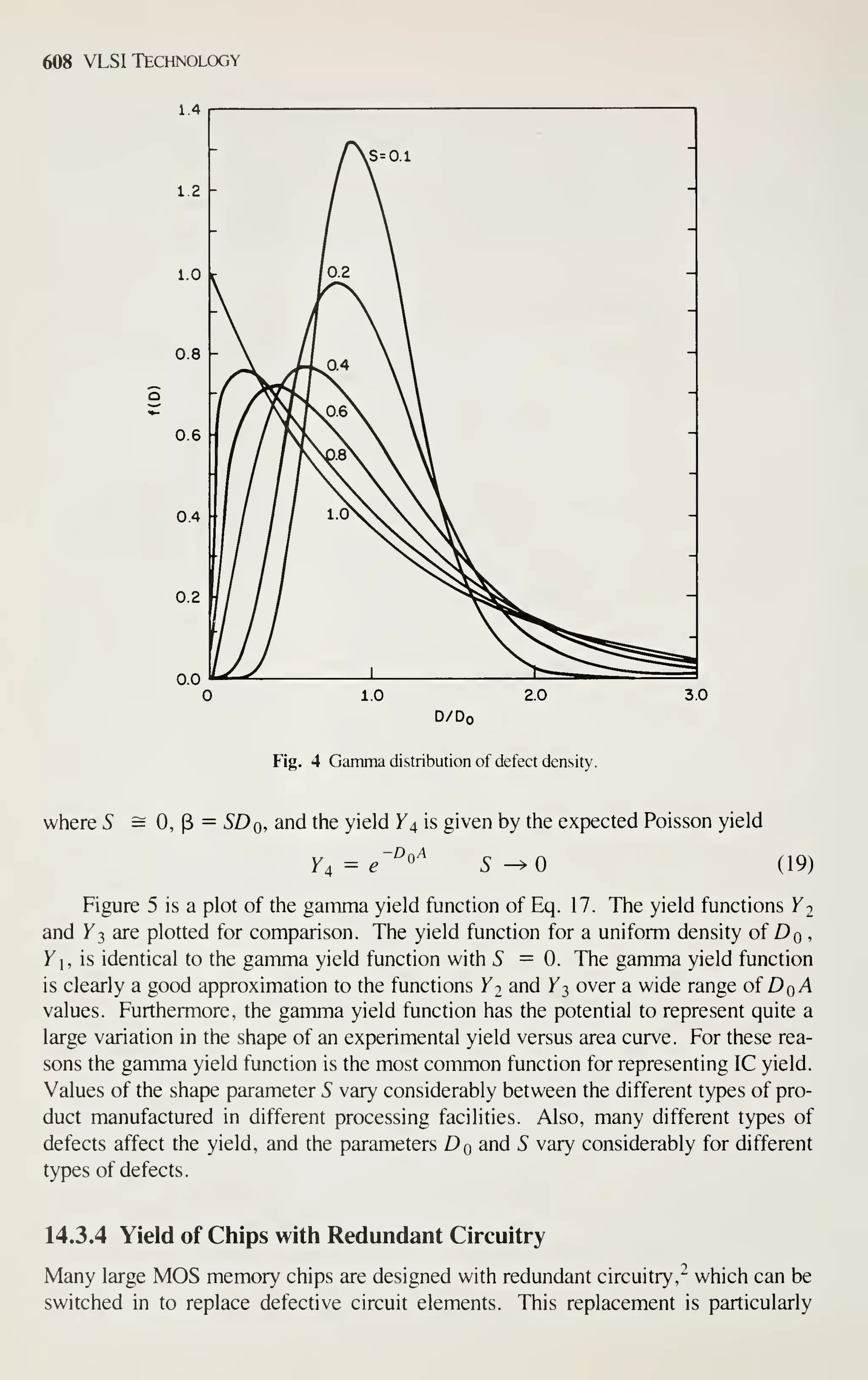
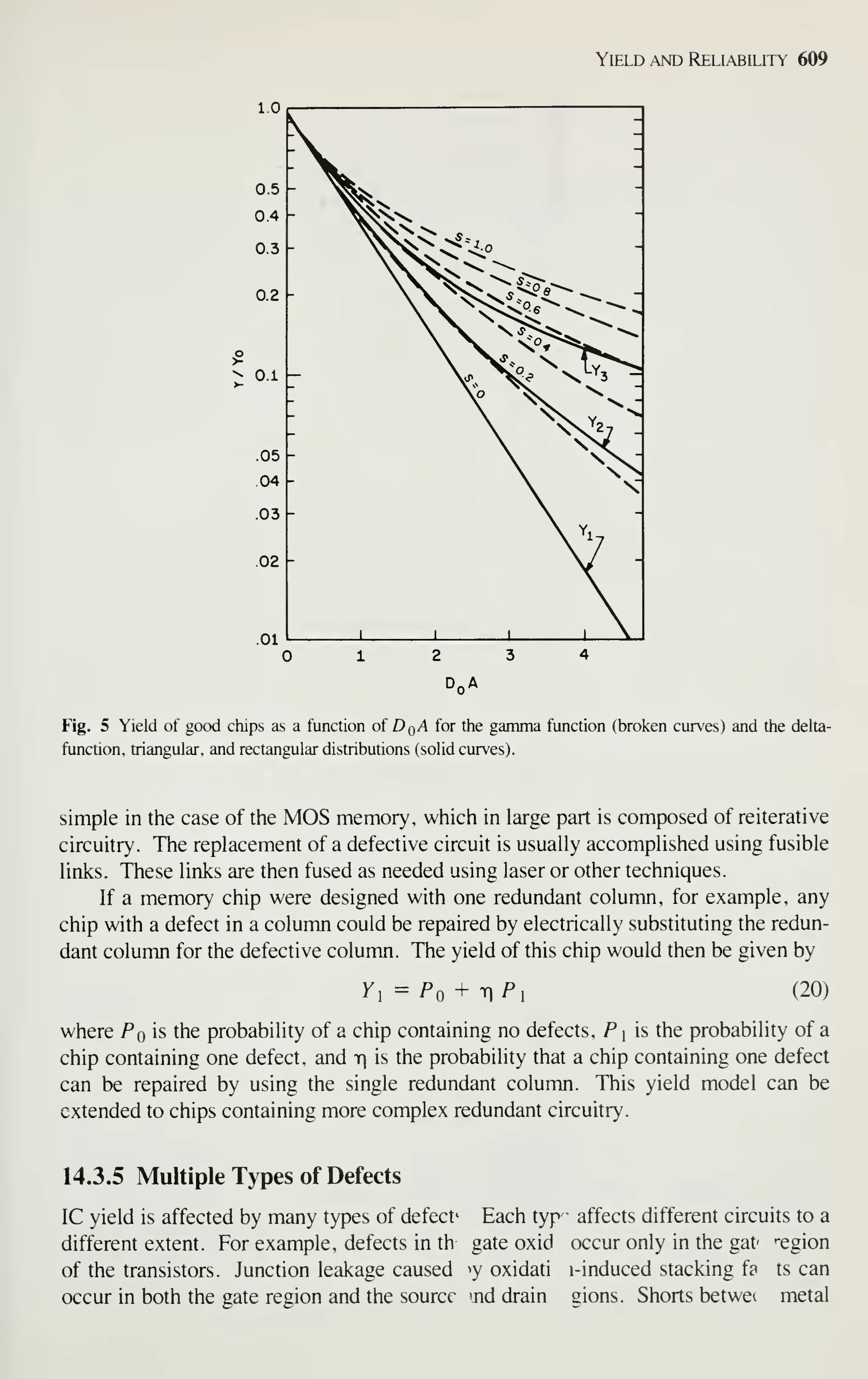
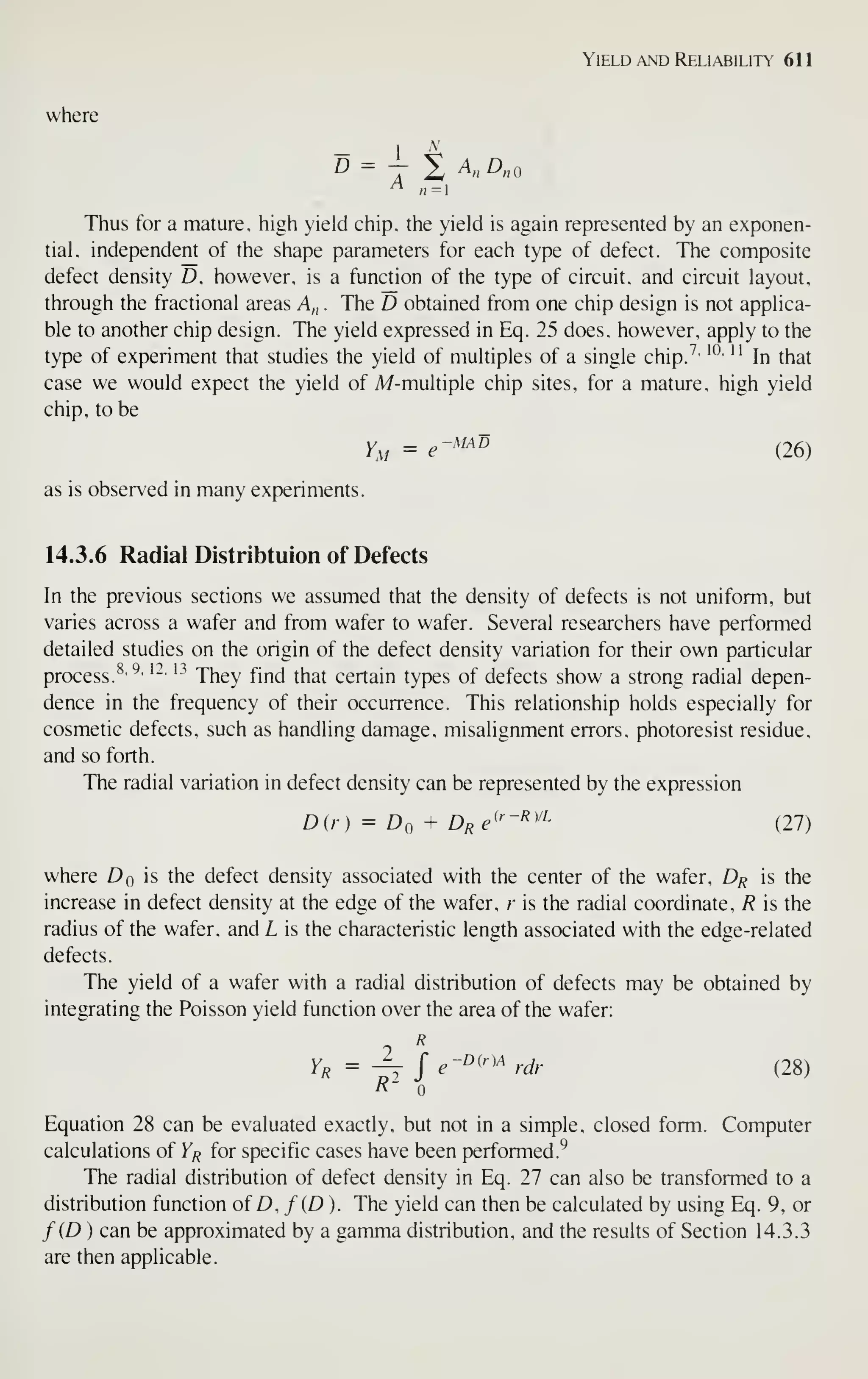
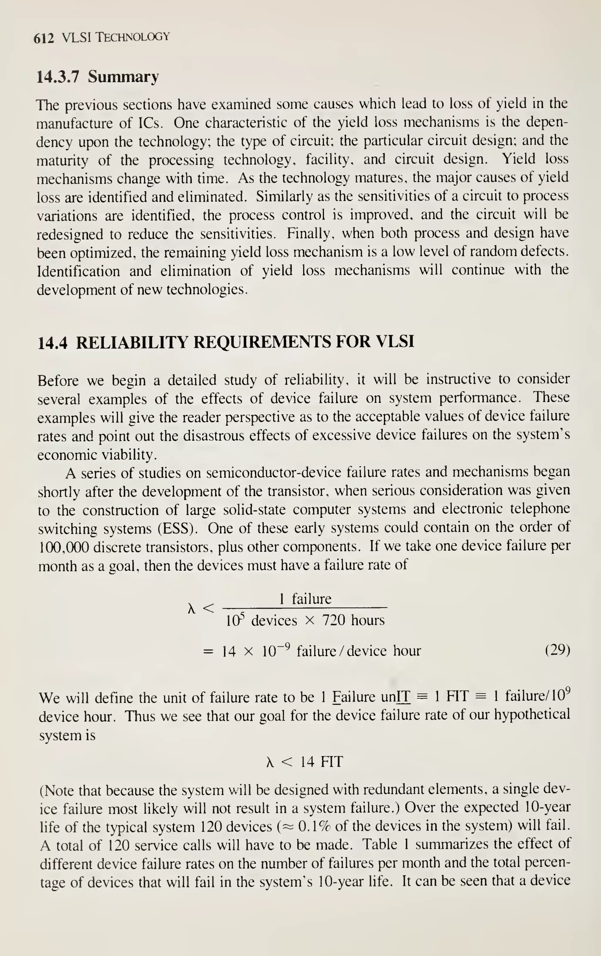
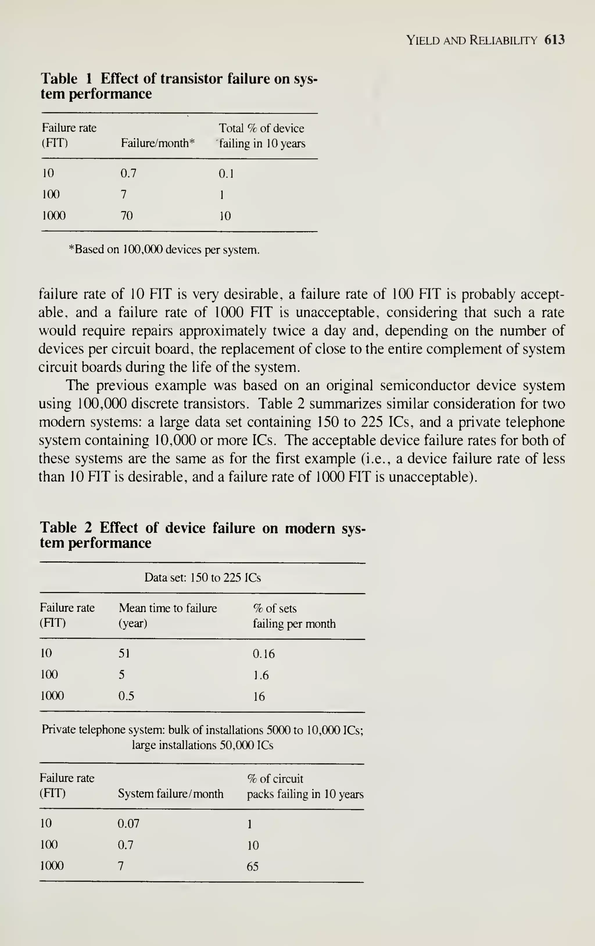
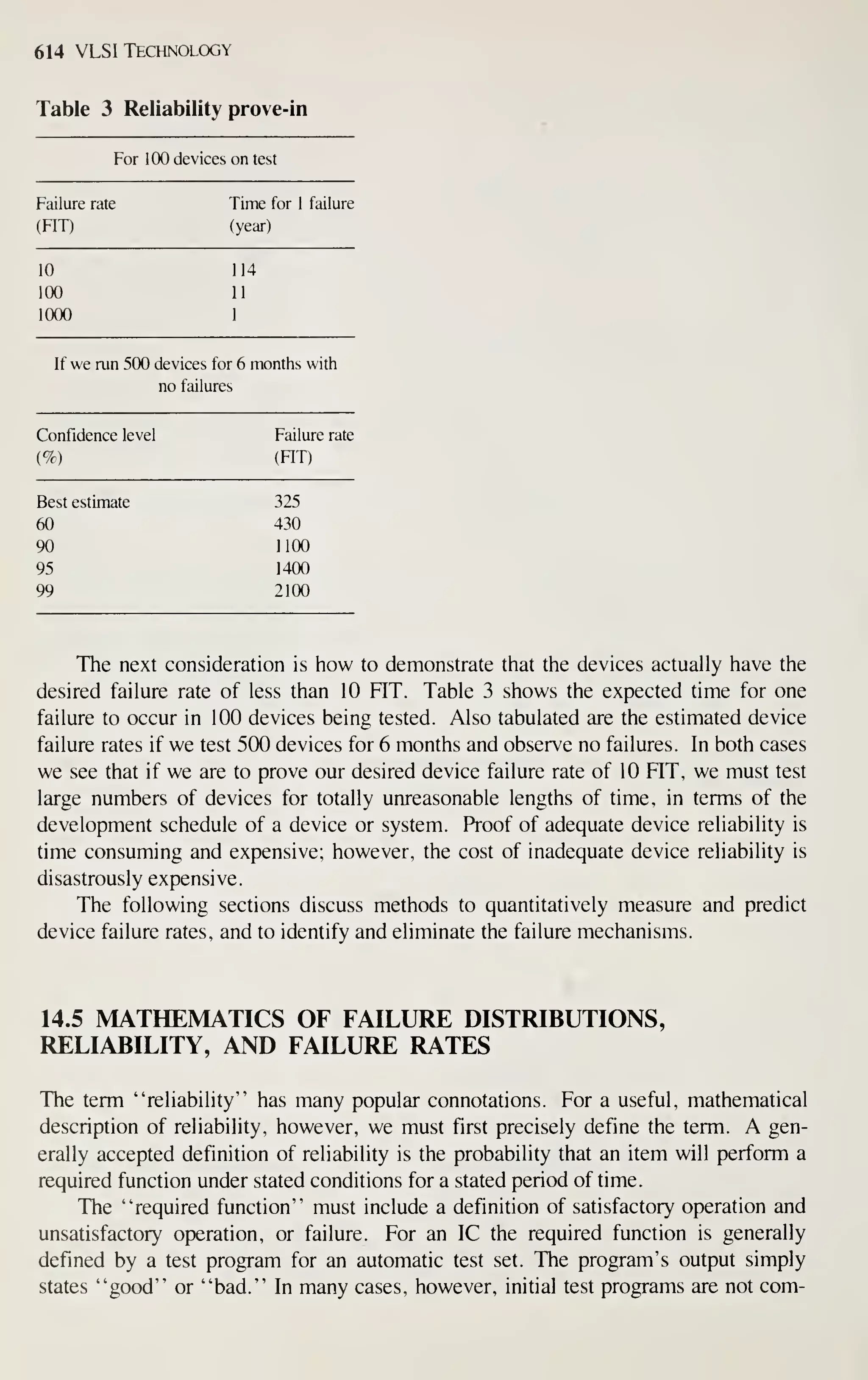
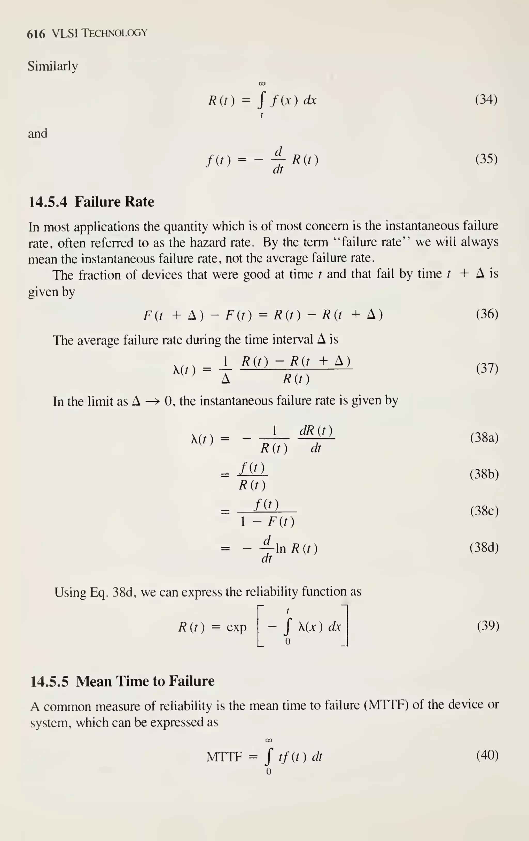
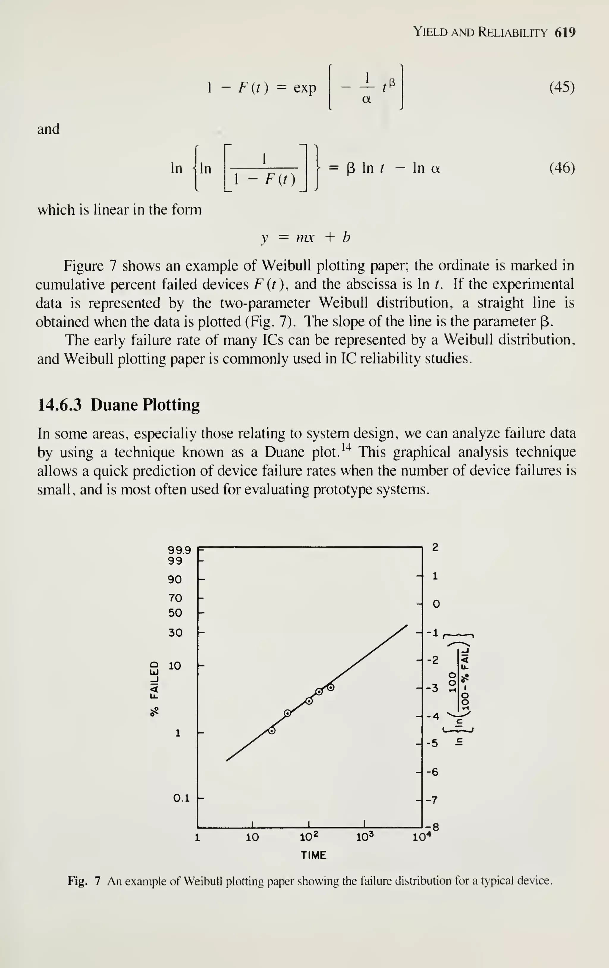
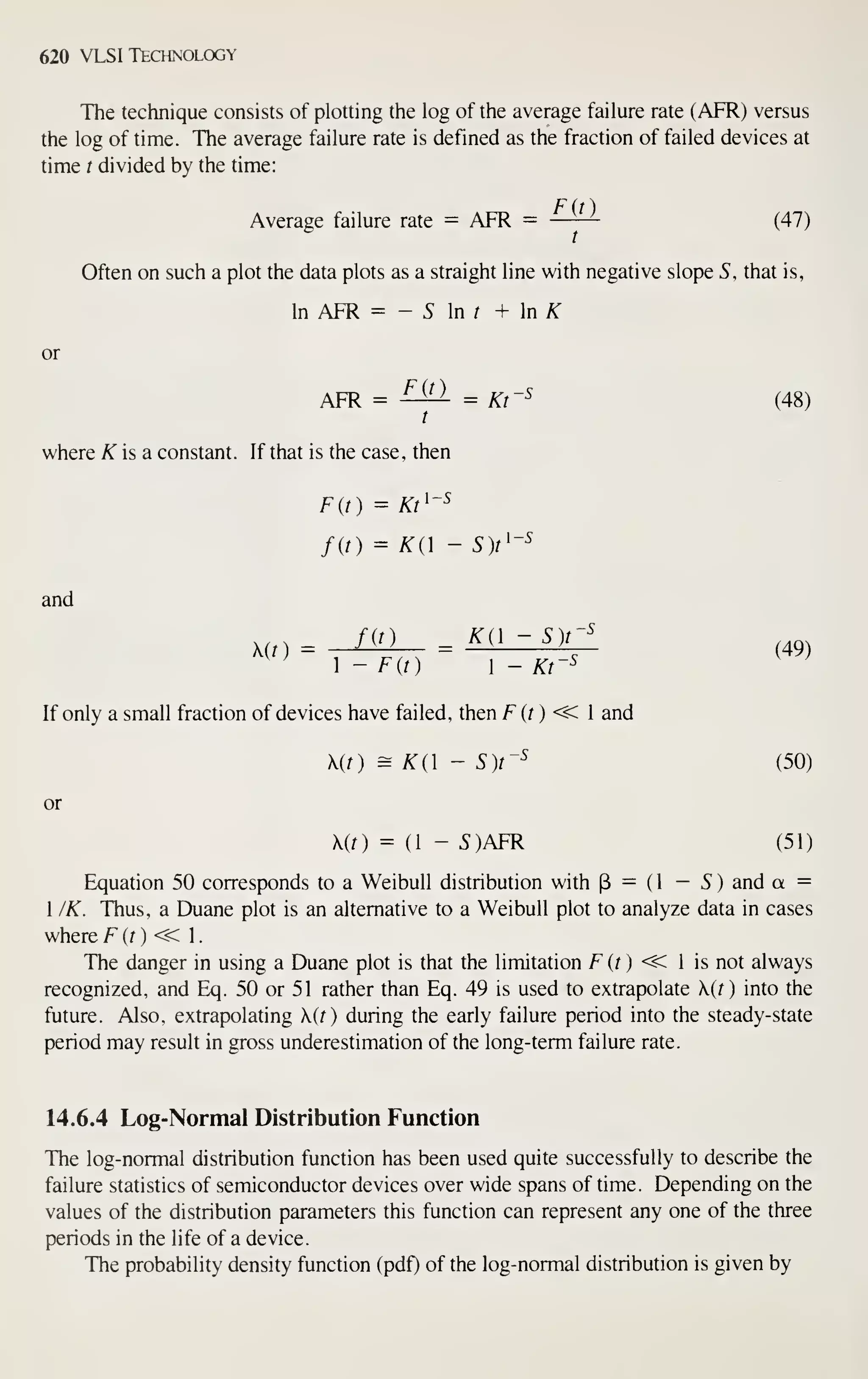
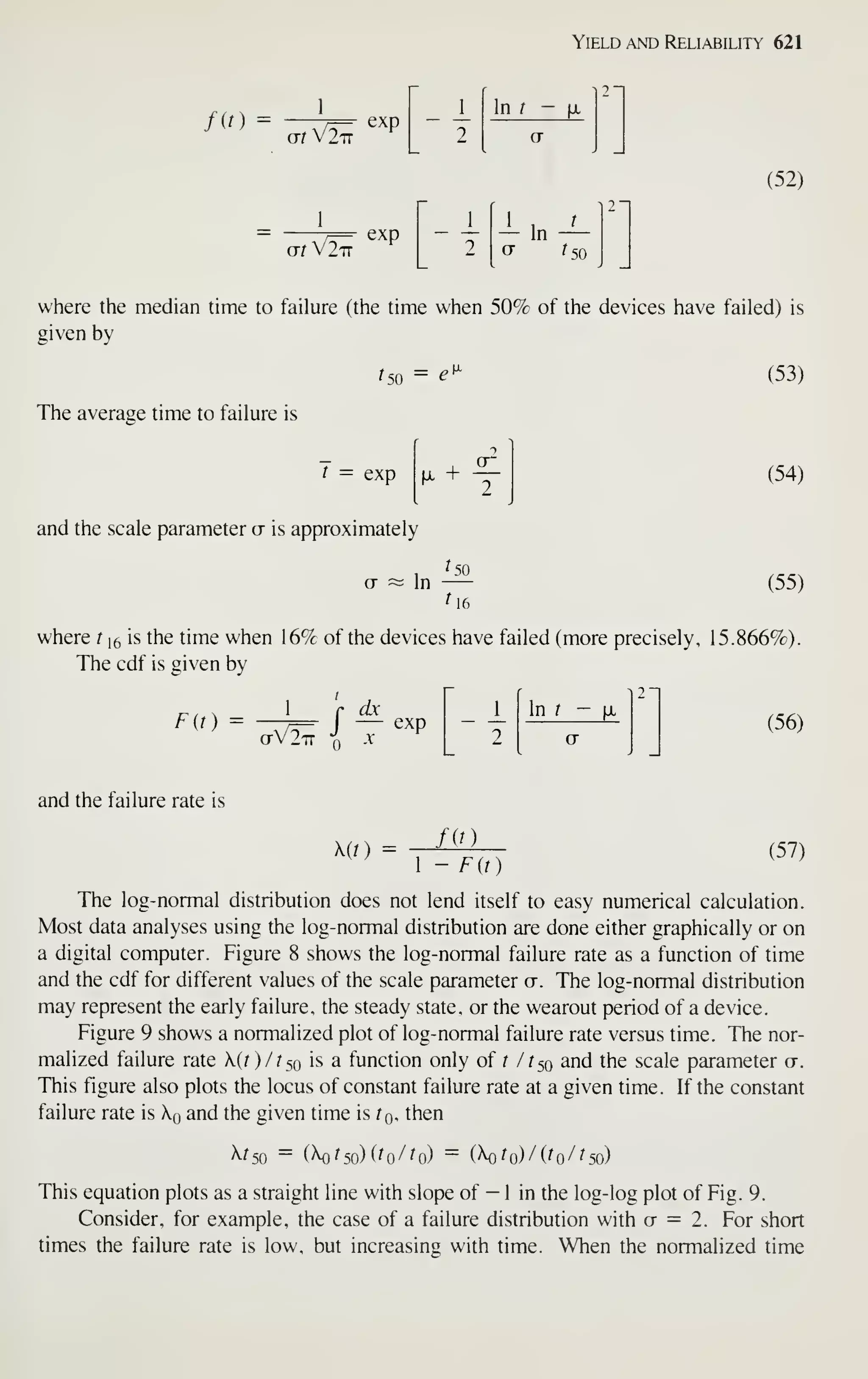
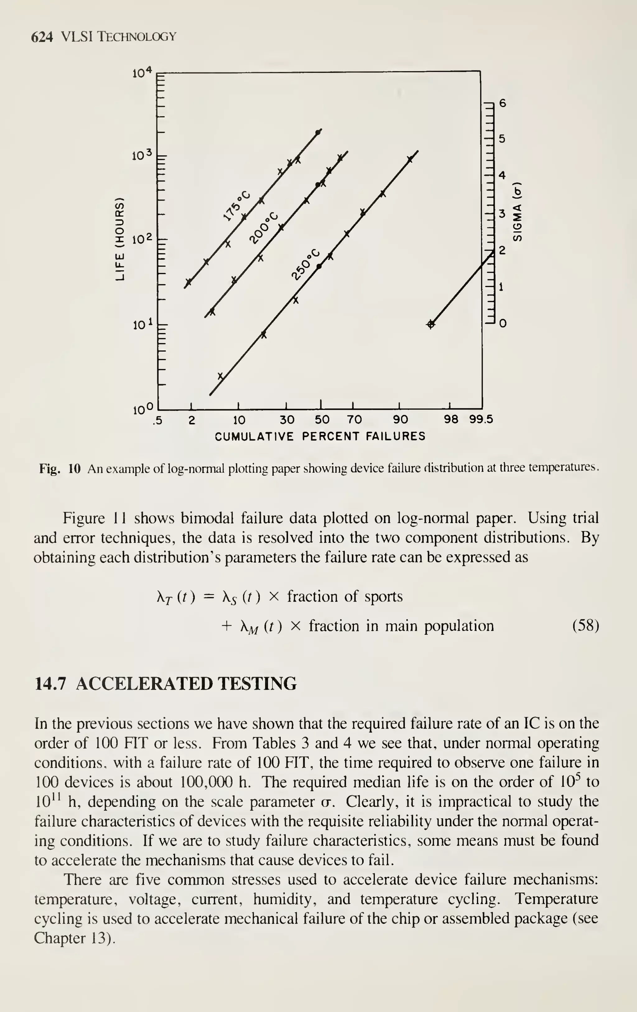
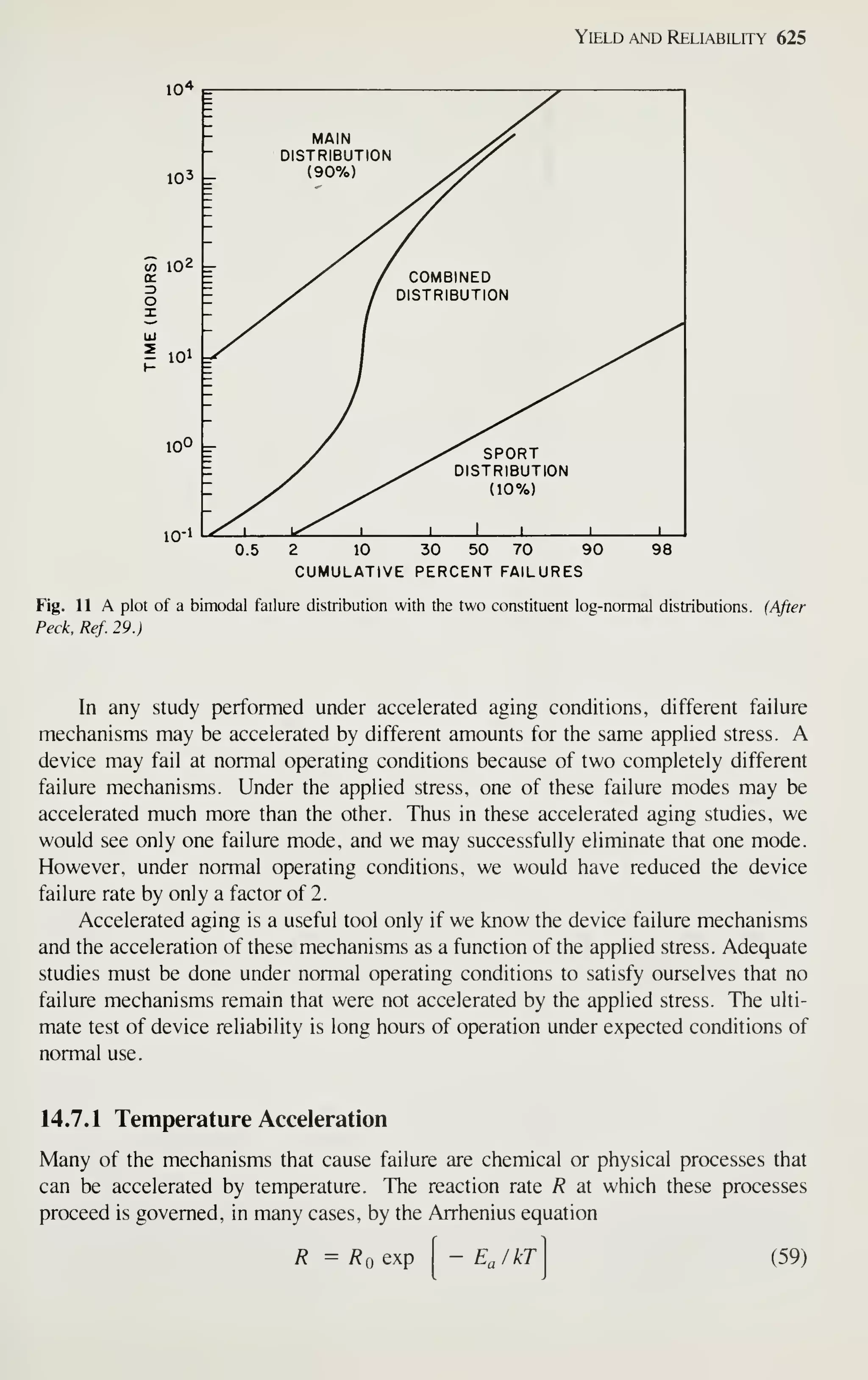
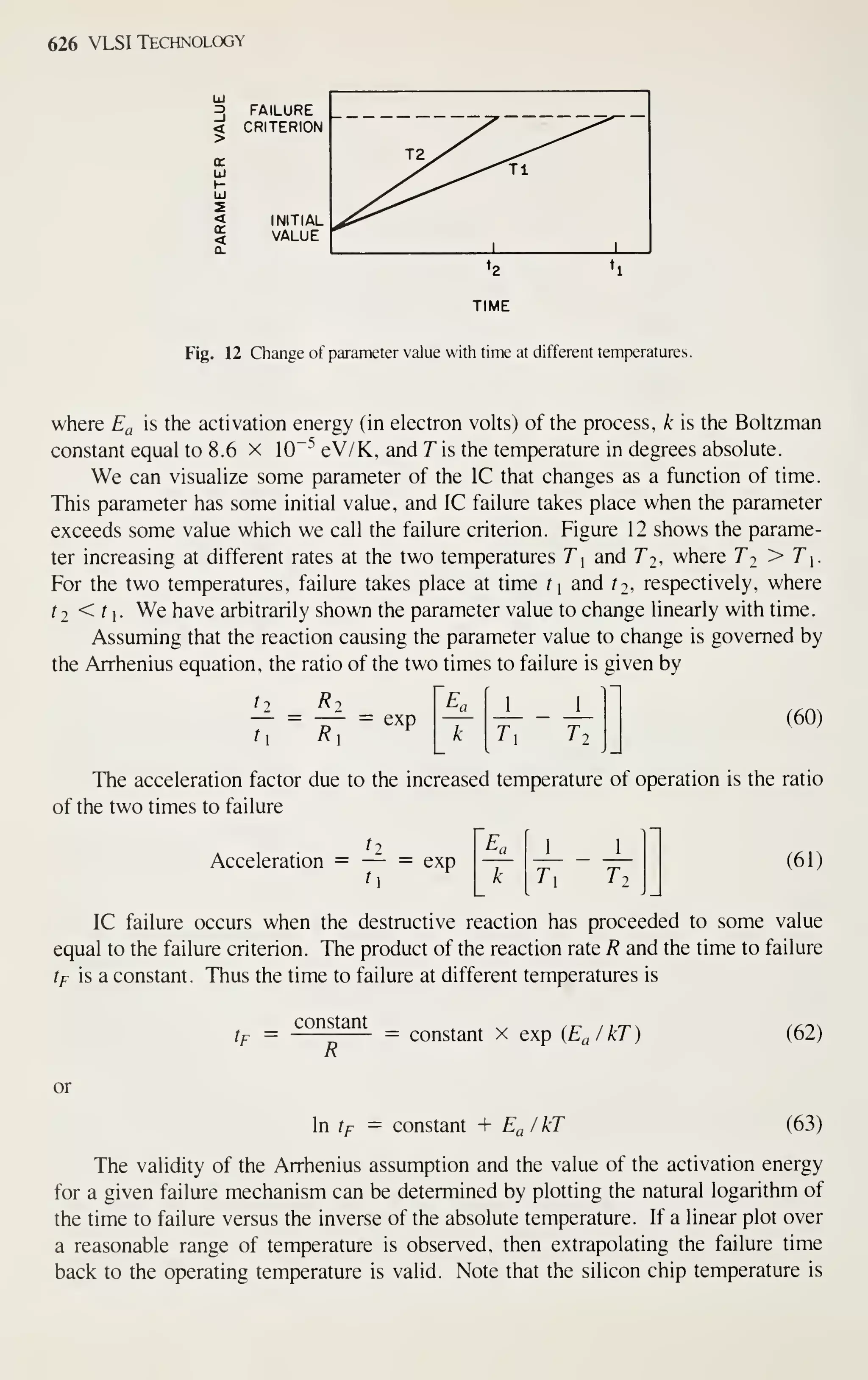
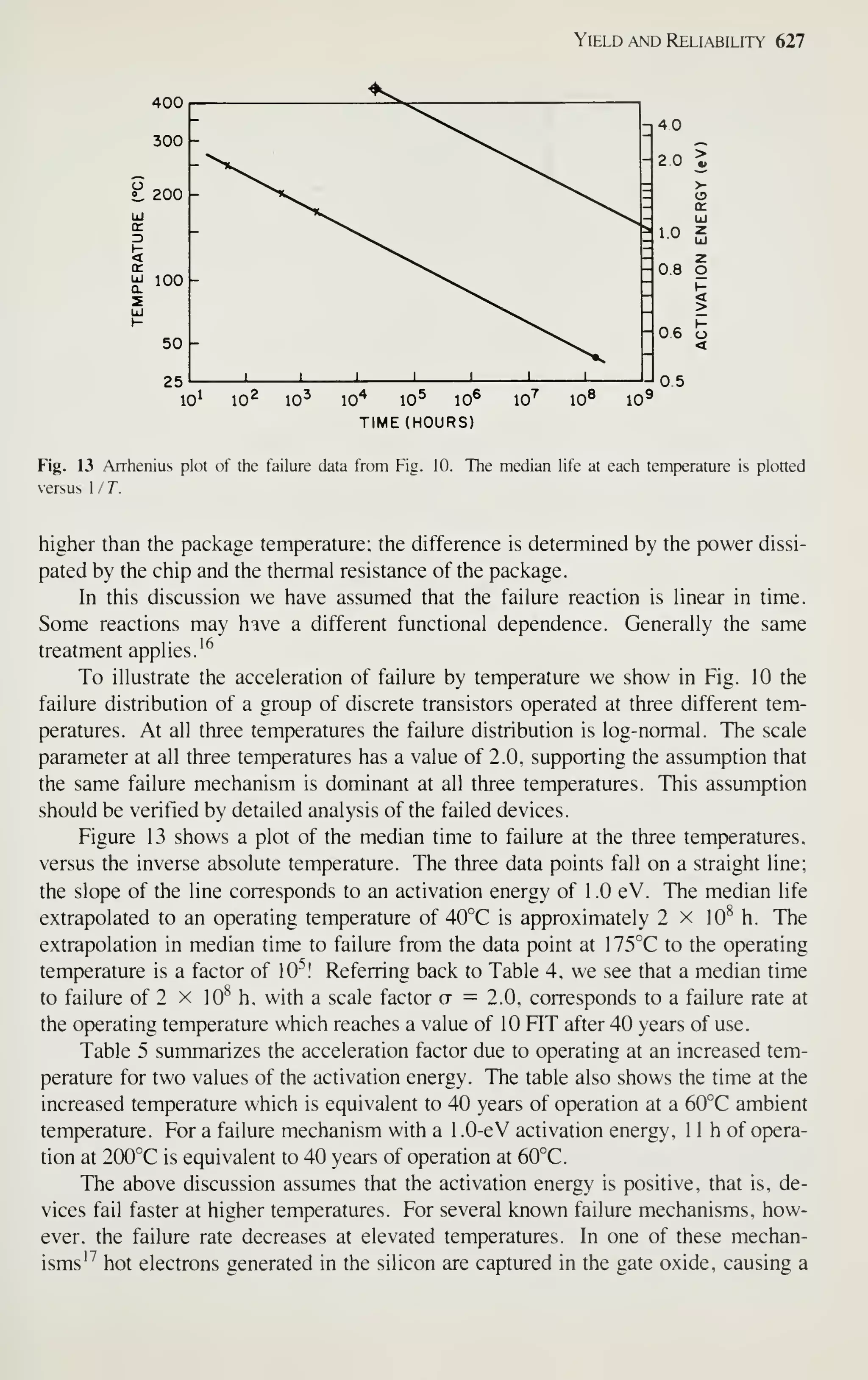
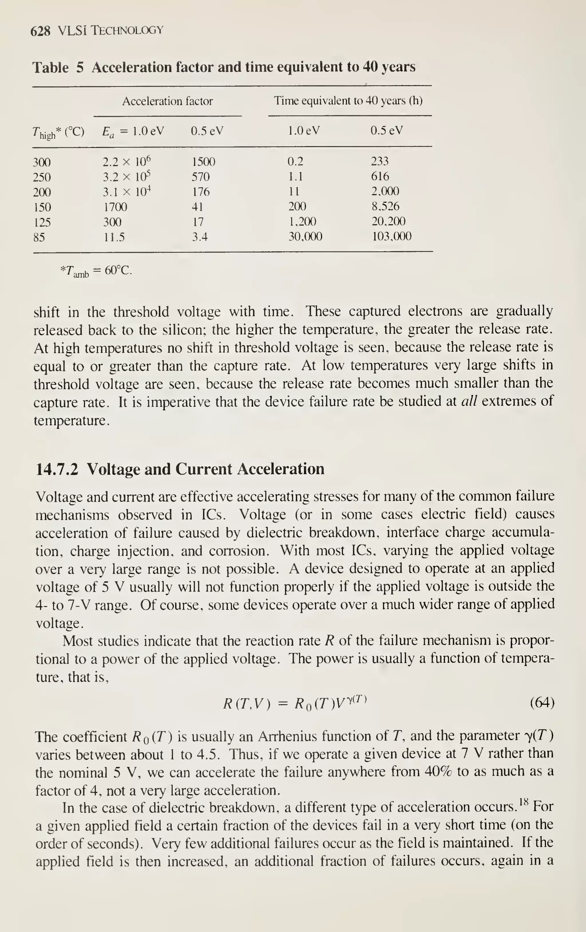
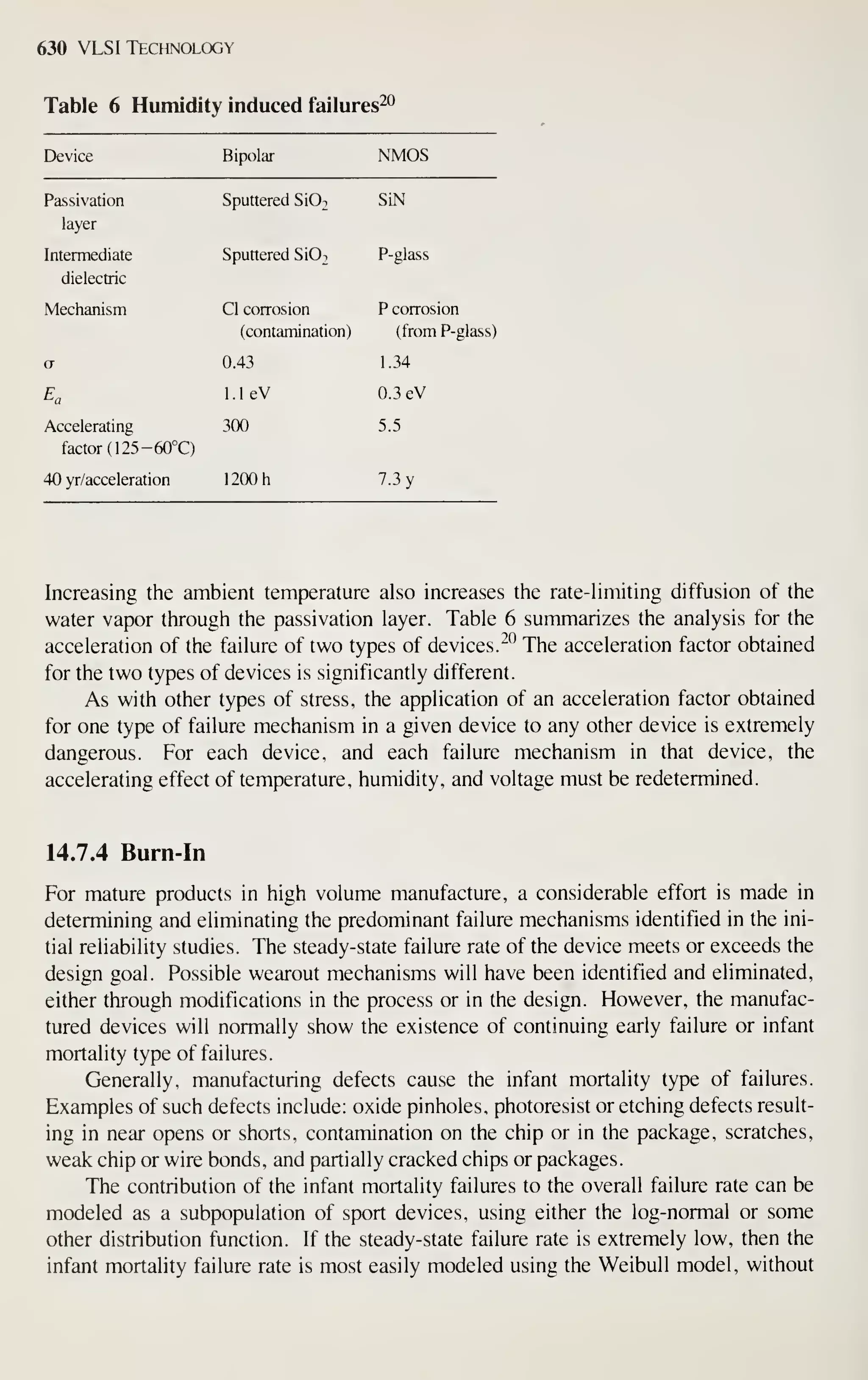
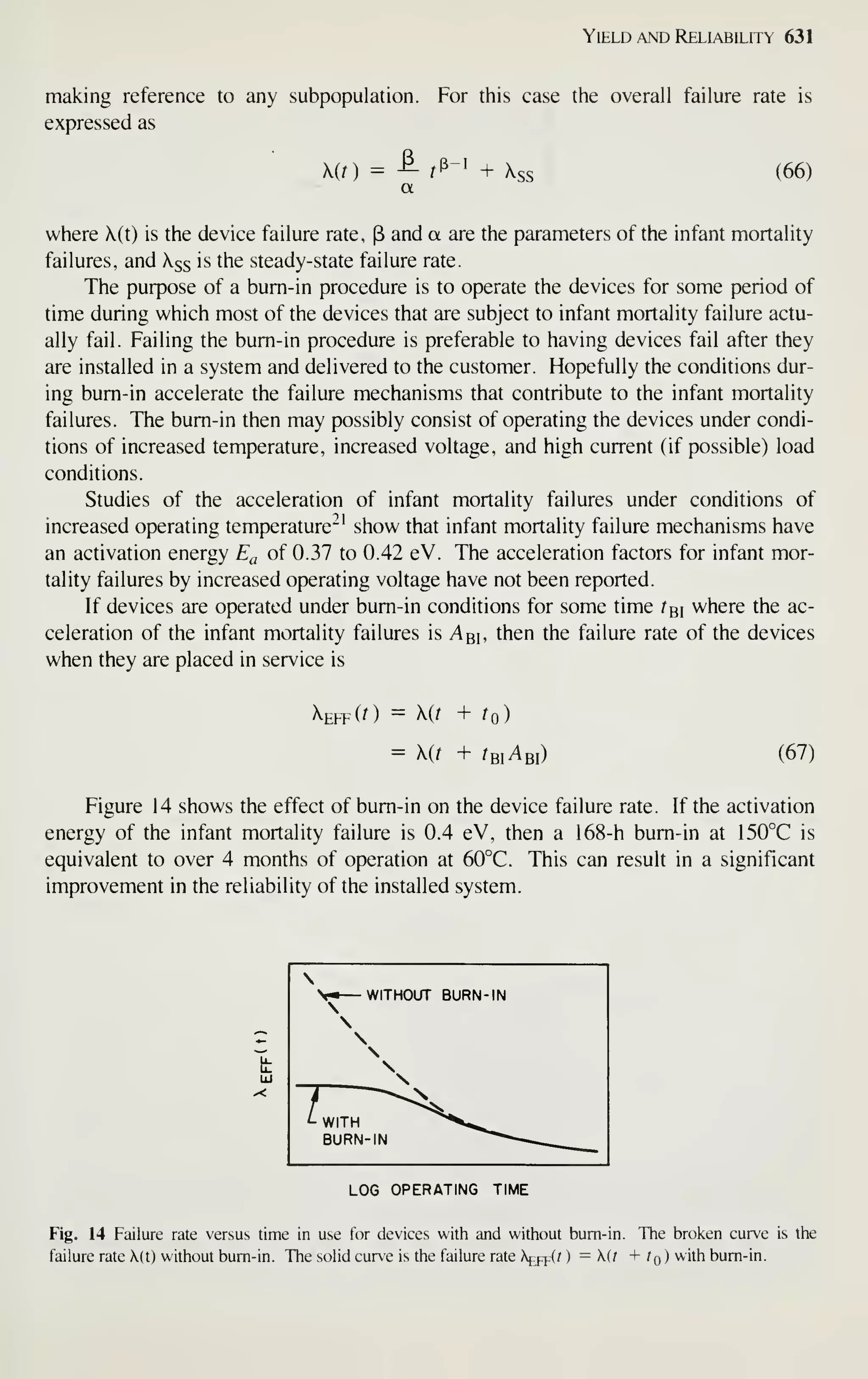
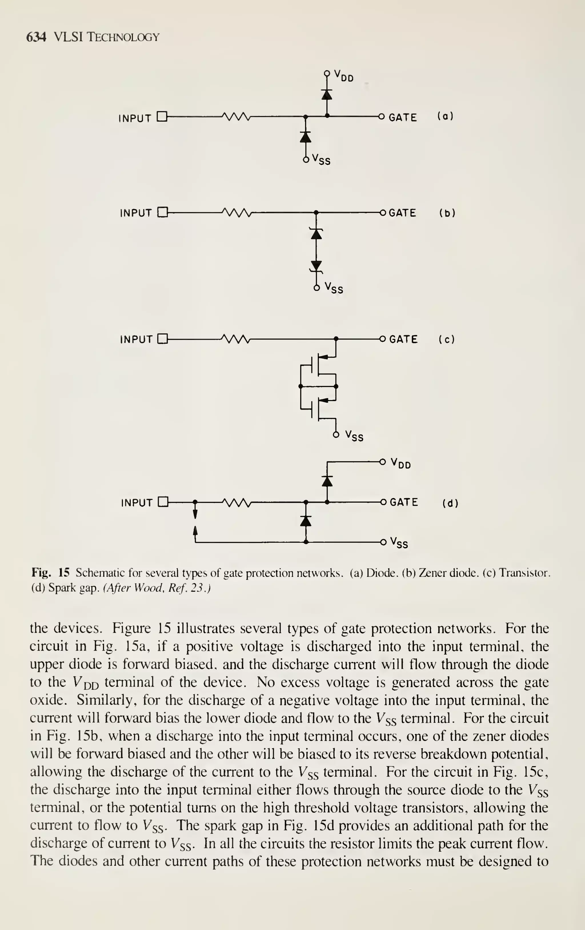
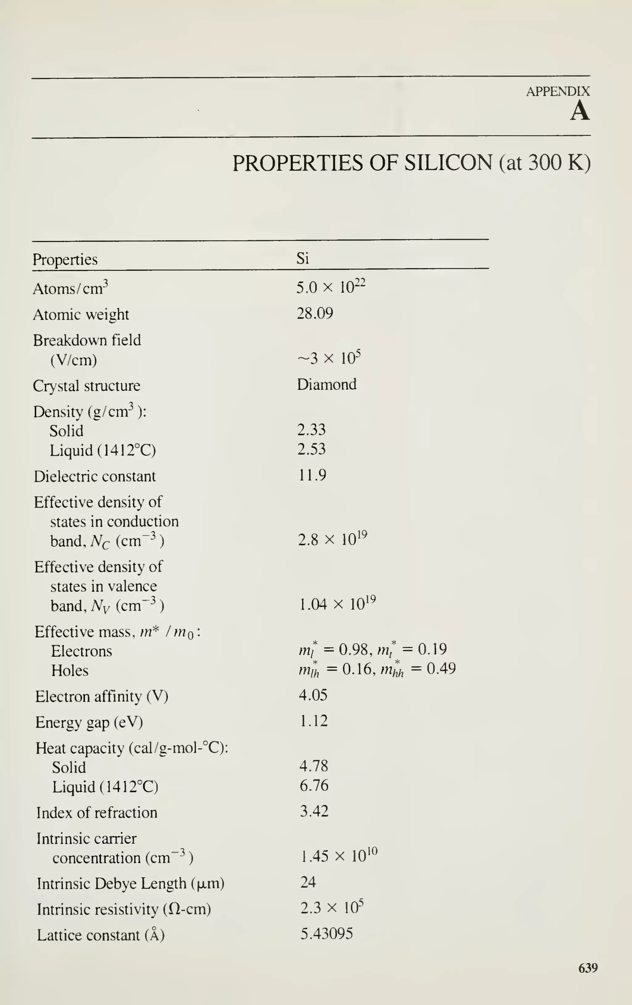
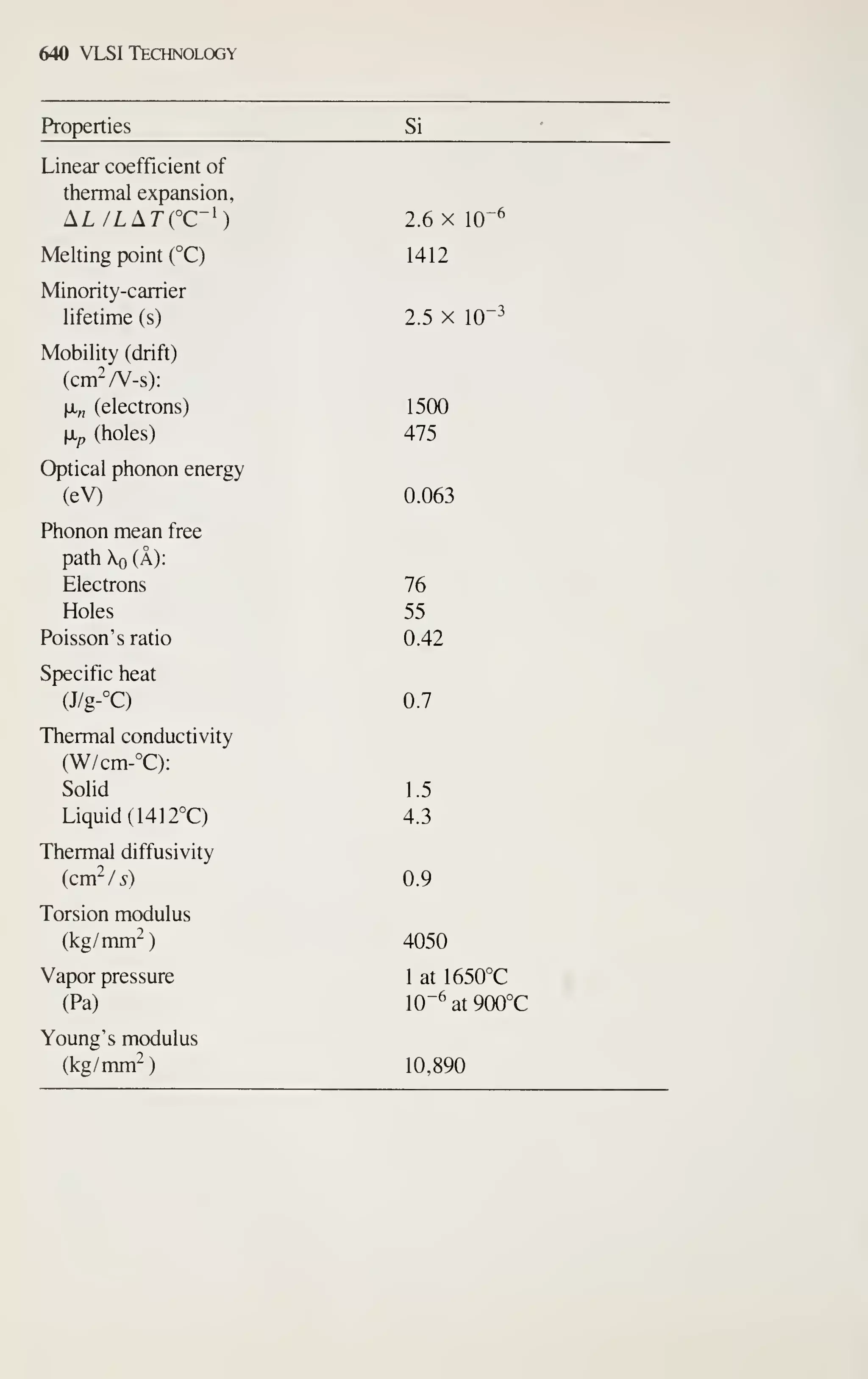
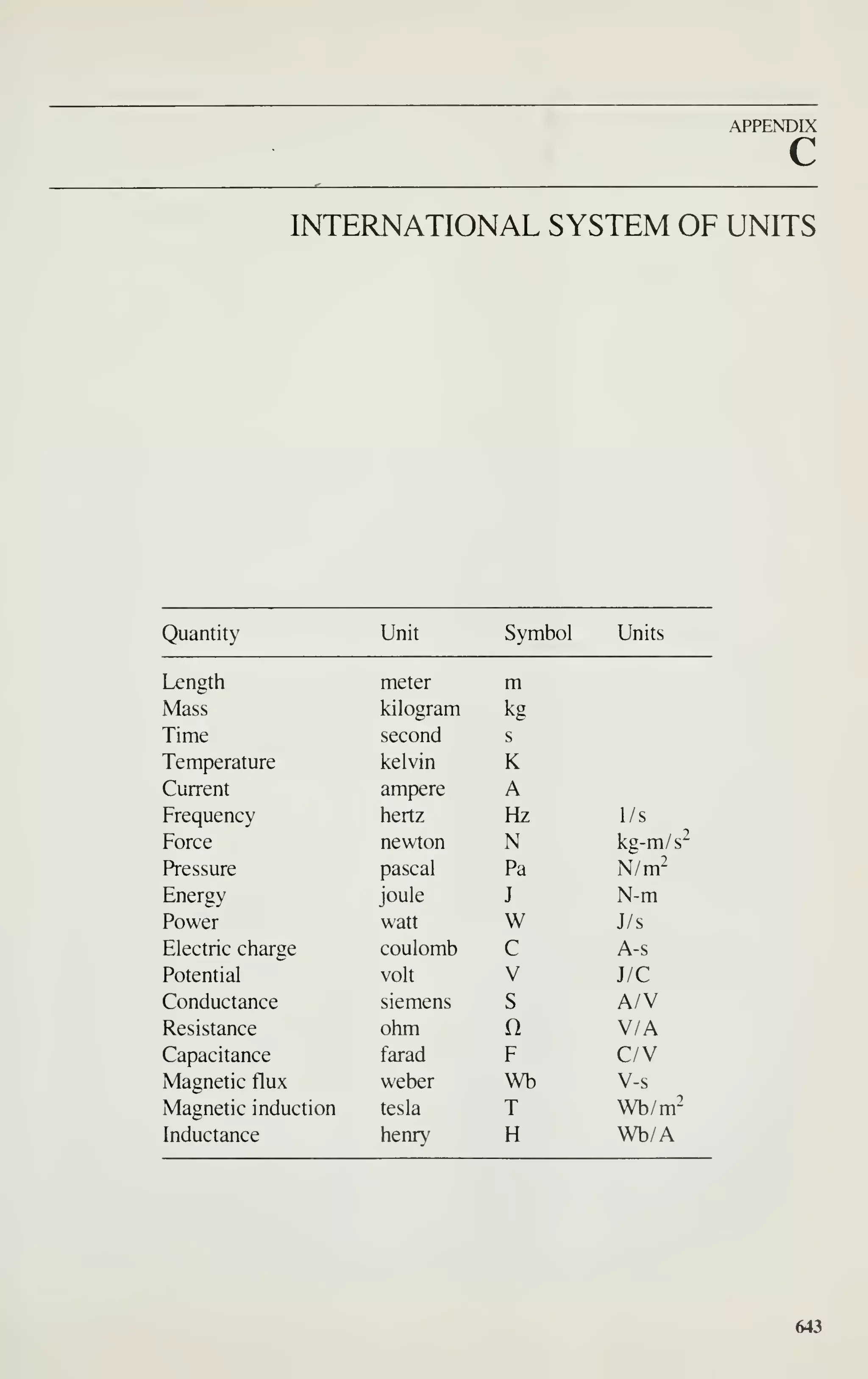


![RF Module Design - [Chapter 4] Transceiver Architecture](https://cdn.slidesharecdn.com/ss_thumbnails/rfch4-150613070346-lva1-app6891-thumbnail.jpg?width=640&height=640&fit=bounds)


