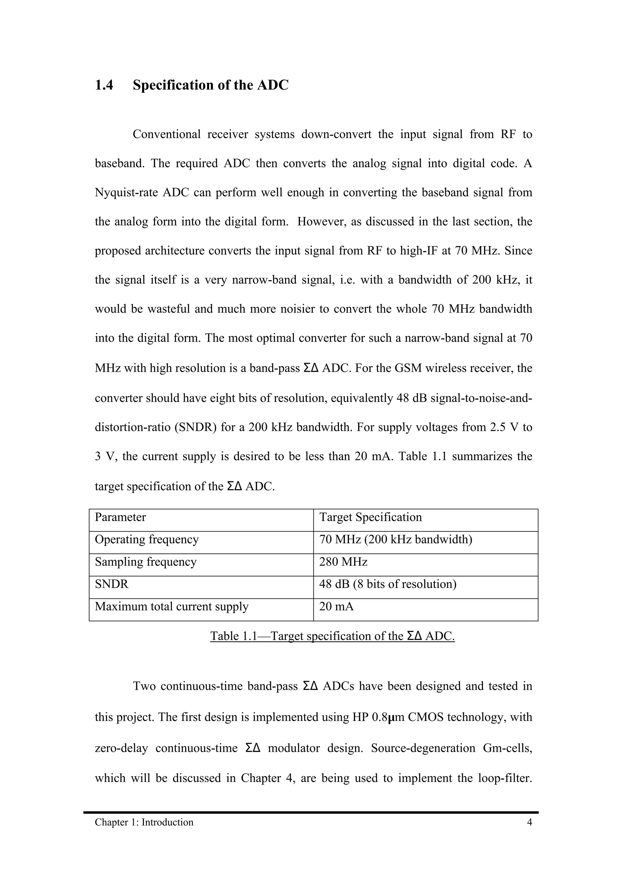
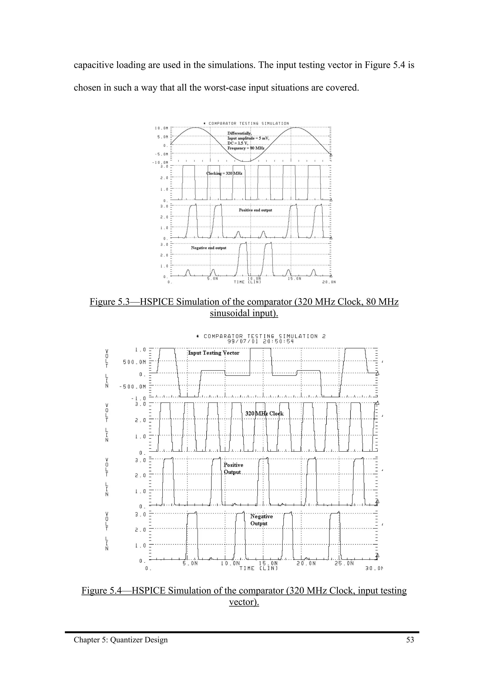
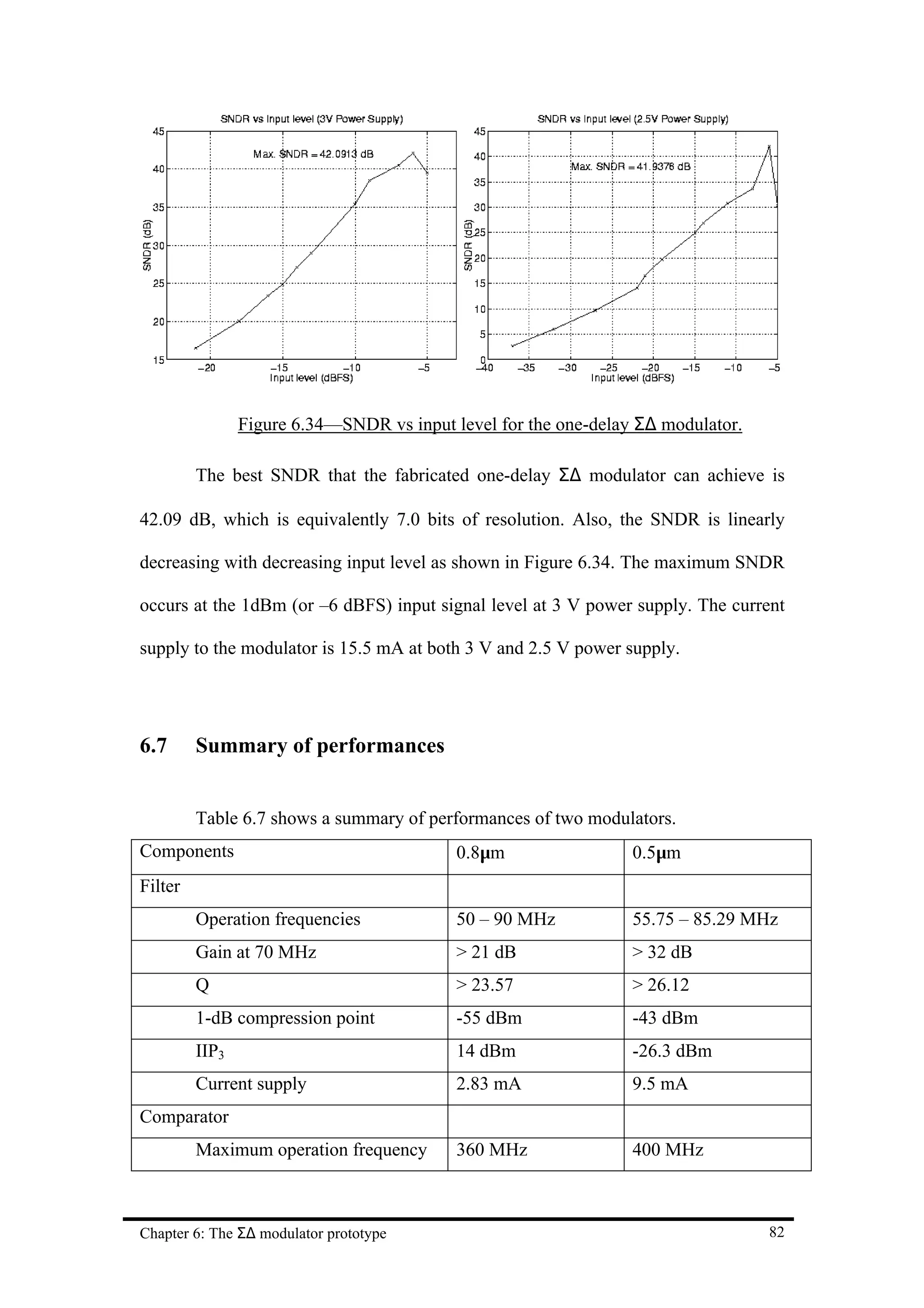
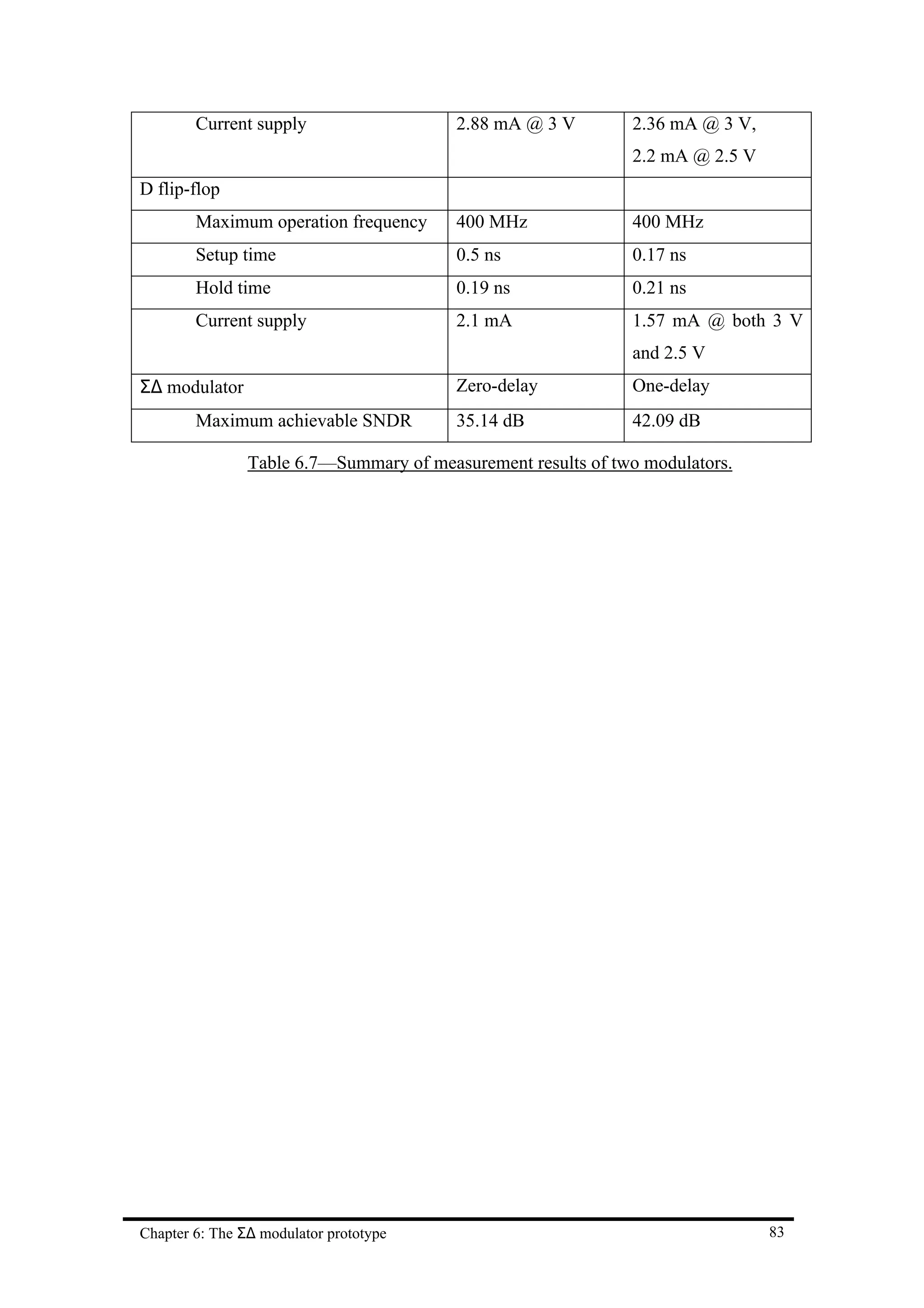
The document describes a thesis submitted by Hsu Kuan Chun Issac to the Hong Kong University of Science and Technology for a Master of Philosophy degree in Electrical and Electronic Engineering. The thesis proposes designing a 70 MHz CMOS band-pass sigma-delta analog-to-digital converter for wireless receivers. It describes implementing a second-order continuous-time band-pass sigma-delta modulator using transconductor-capacitor integrators for the loop filter. The design includes a latched comparator and TSPC D flip-flop as the quantizer. The performance of prototypes fabricated in 0.8um and 0.5um CMOS processes are evaluated.
![List of Figures
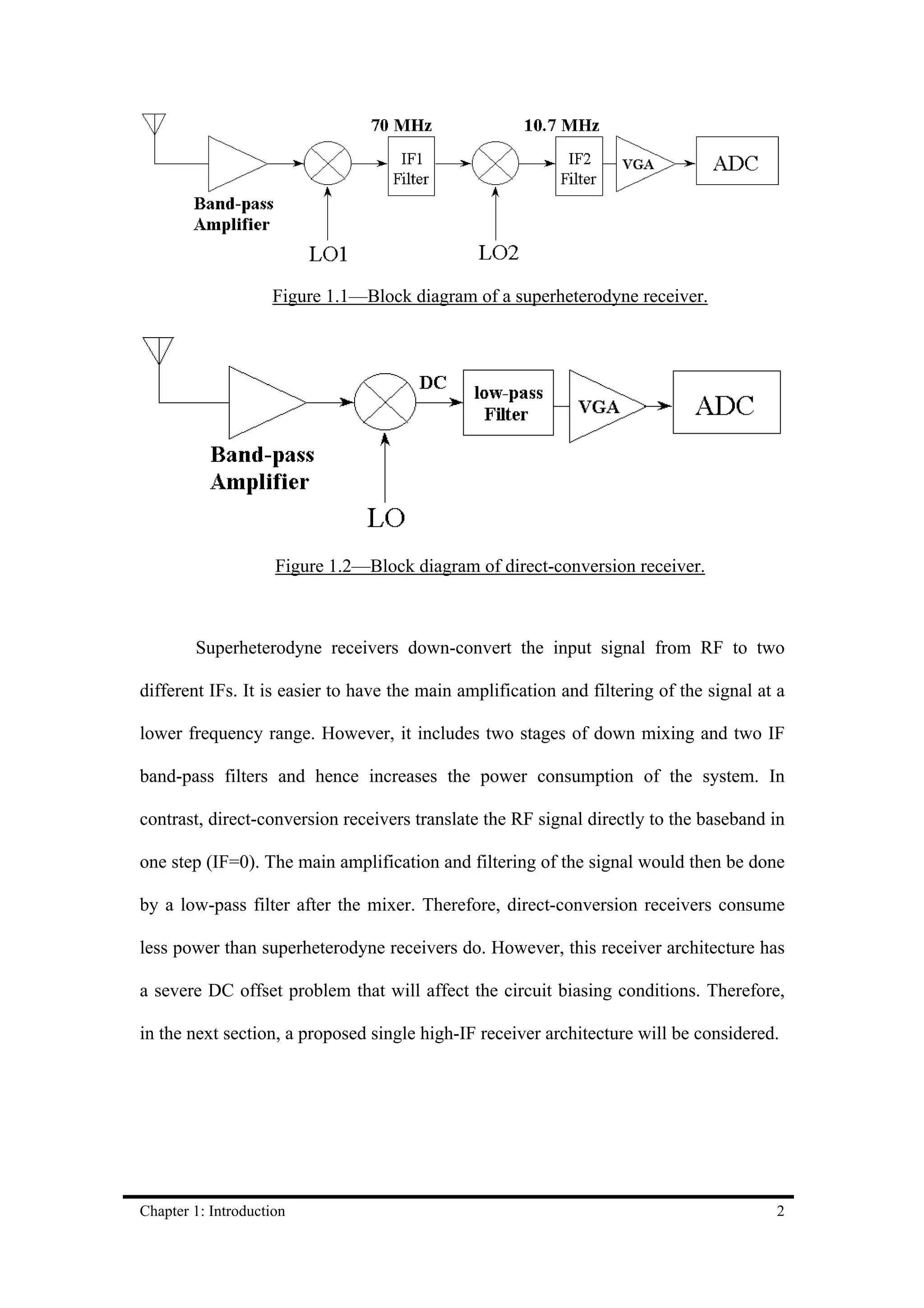
Figure 1.1—Block diagram of a superheterodyne receiver. 2
Figure 1.2—Block diagram of direct-conversion receiver. 2
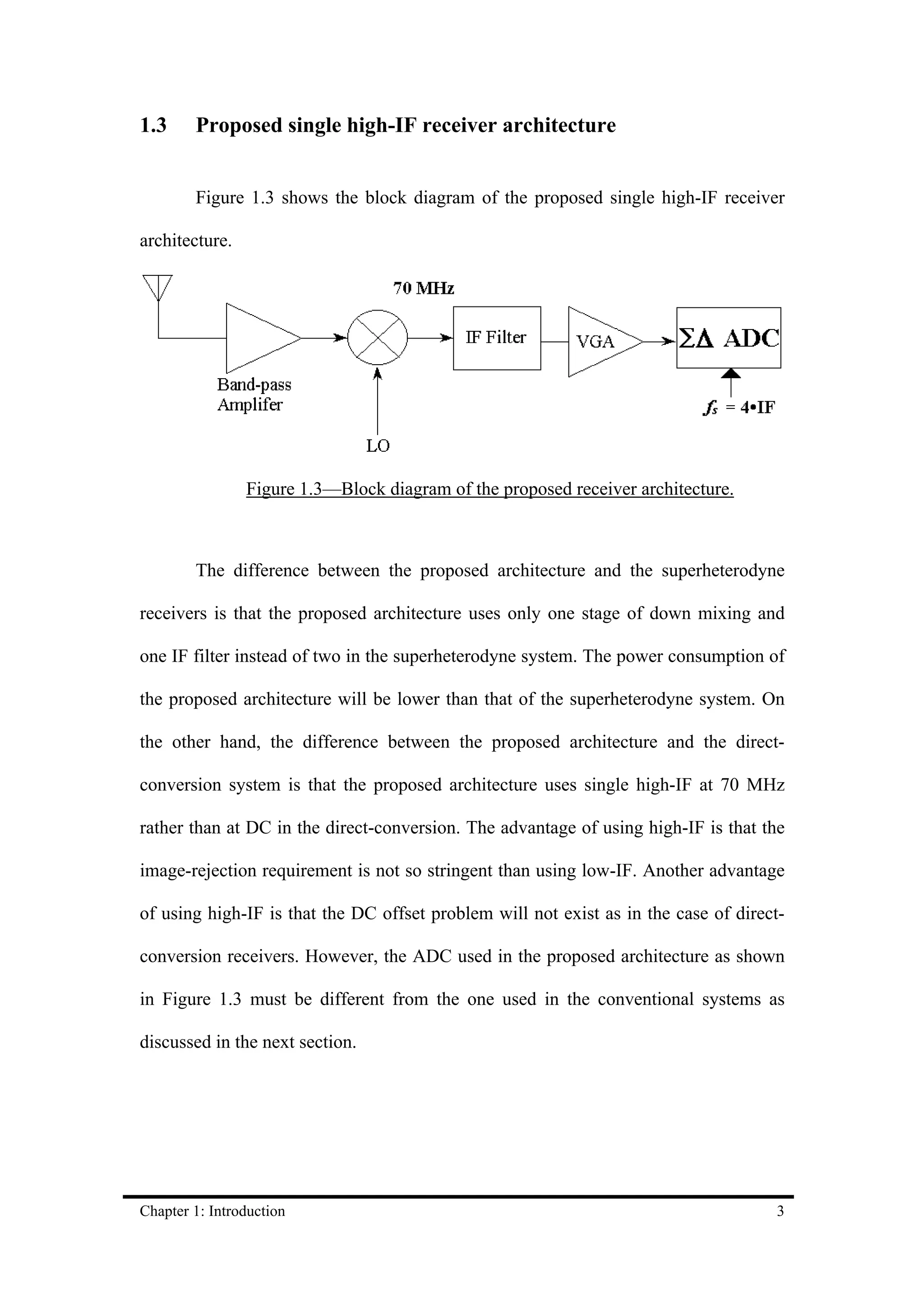
Figure 1.3—Block diagram of the proposed receiver architecture. 3
Figure 2.1–Conventional Nyquist-rate ADC blocks [1]. 6
Figure 2.2–An example of a uniform multilevel quantization characteristic that is represented by
linear gain G and an error e [1]. 8
Figure 2.3–Quantization noise power spectral density for Nyquist rate and oversampled
conversion [2]. 10
Figure 2.4—Block diagram of a Σ∆ modulator. 11
Figure 2.5—Linearized model of the quantizer. 12
Figure 2.6–Block diagram of a first-order Σ∆ modulator. 12
Figure 2.7—Linearized model block diagram of a first-order Σ∆ modulator. 12
Figure 2.8–First-order Noise Transfer Function (NTF) magnitude spectrum in dB. 13
Figure 2.9–Quantization Noise Spectrum. (a) Before first-order low-pass Σ∆ noise-shaping, (b)
After first-order low-pass Σ∆ noise-shaping. 14
Figure 2.10–Block Diagram of a second-order band-pass Σ∆ modulator. 16
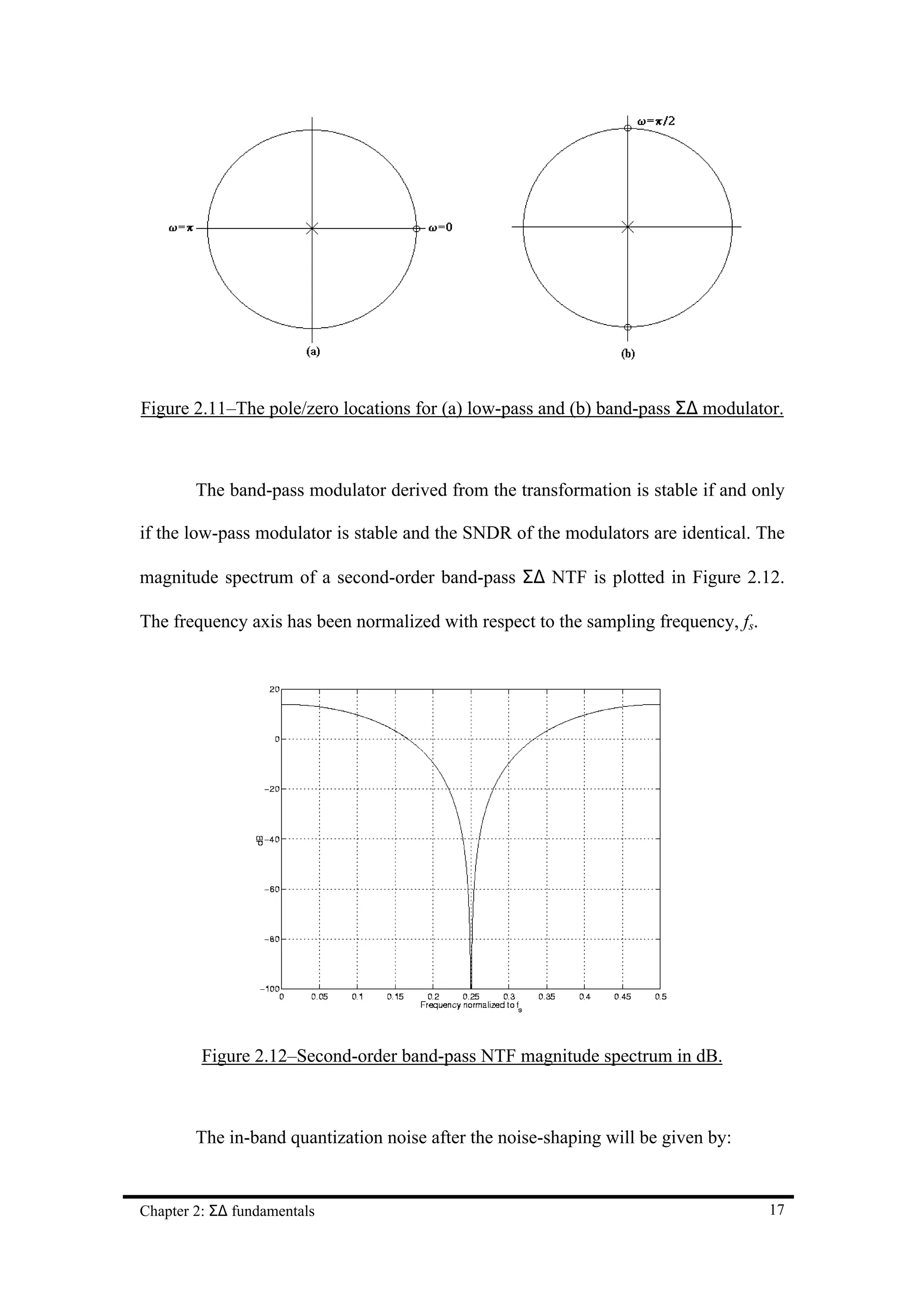
Figure 2.11–The pole/zero locations for (a) low-pass and (b) band-pass Σ∆ modulator. 17
Figure 2.12–Second-order band-pass NTF magnitude spectrum in dB. 17
Figure 2.13–Quantization Noise Spectrum. (a) Before second-order band-pass Σ∆ noise-shaping,
(b) After second-order band-pass Σ∆ noise-shaping. 18
Figure 2.14–Block Diagram of a continuous-time Σ∆ modulator. 20
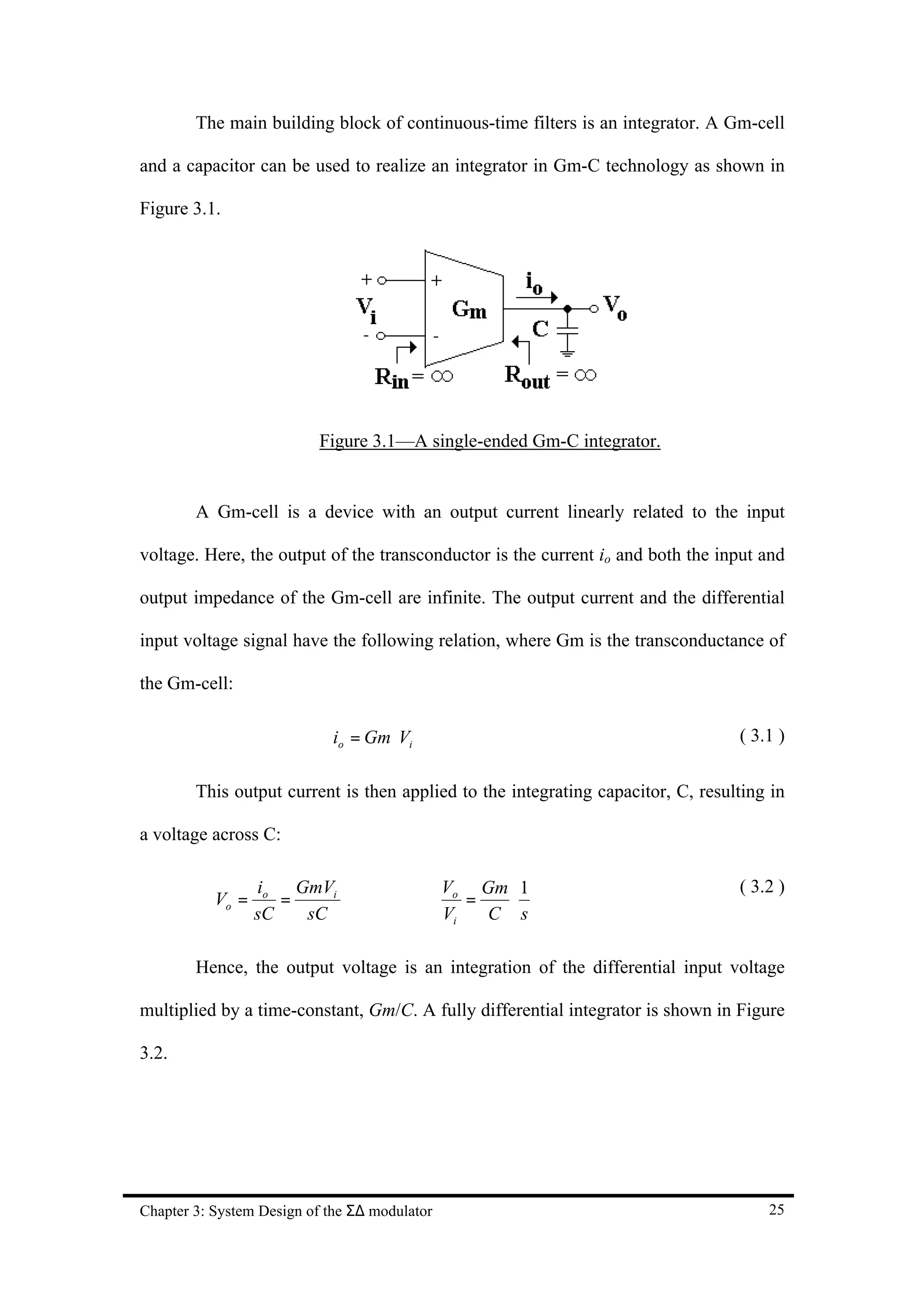
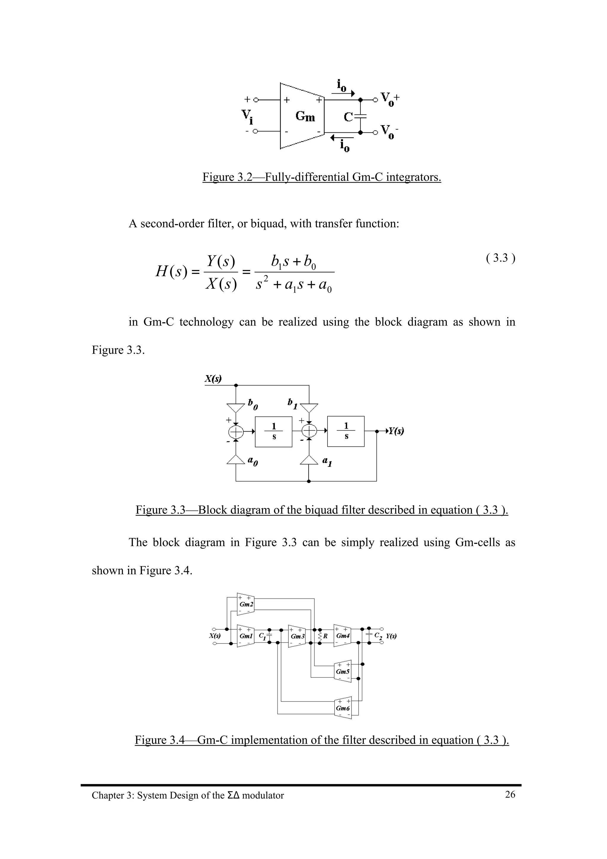
Figure 3.1—A single-ended Gm-C integrator. 25
Figure 3.2—Fully-differential Gm-C integrators. 26
Figure 3.3—Block diagram of the biquad filter described in equation ( 3.3 ). 26
Figure 3.4—Gm-C implementation of the filter described in equation ( 3.3 ). 26
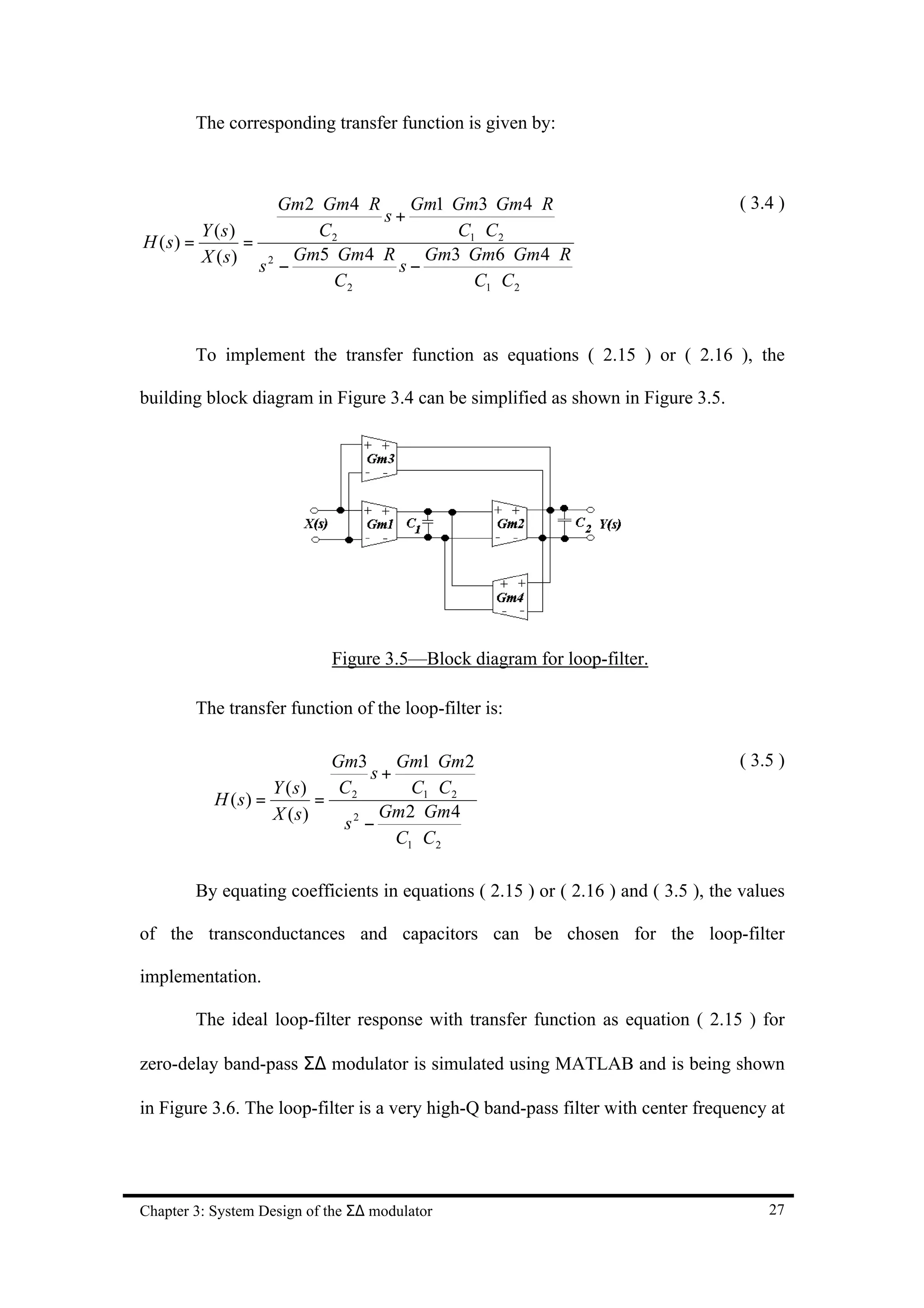
Figure 3.5—Block diagram for loop-filter. 27
Figure 3.6—Ideal magnitude and phase response of the loop-filter described in equation ( 2.15 ).
28
Figure 3.7—HSPICE simulation of the loop-filter described in equation ( 2.15 ). 29
Figure 3.8—Ideal magnitude and phase response of the loop-filter described in equation ( 2.16 ).
29
Figure 3.9— HSPICE simulation of the loop-filter described in equation ( 2.16 ). 30
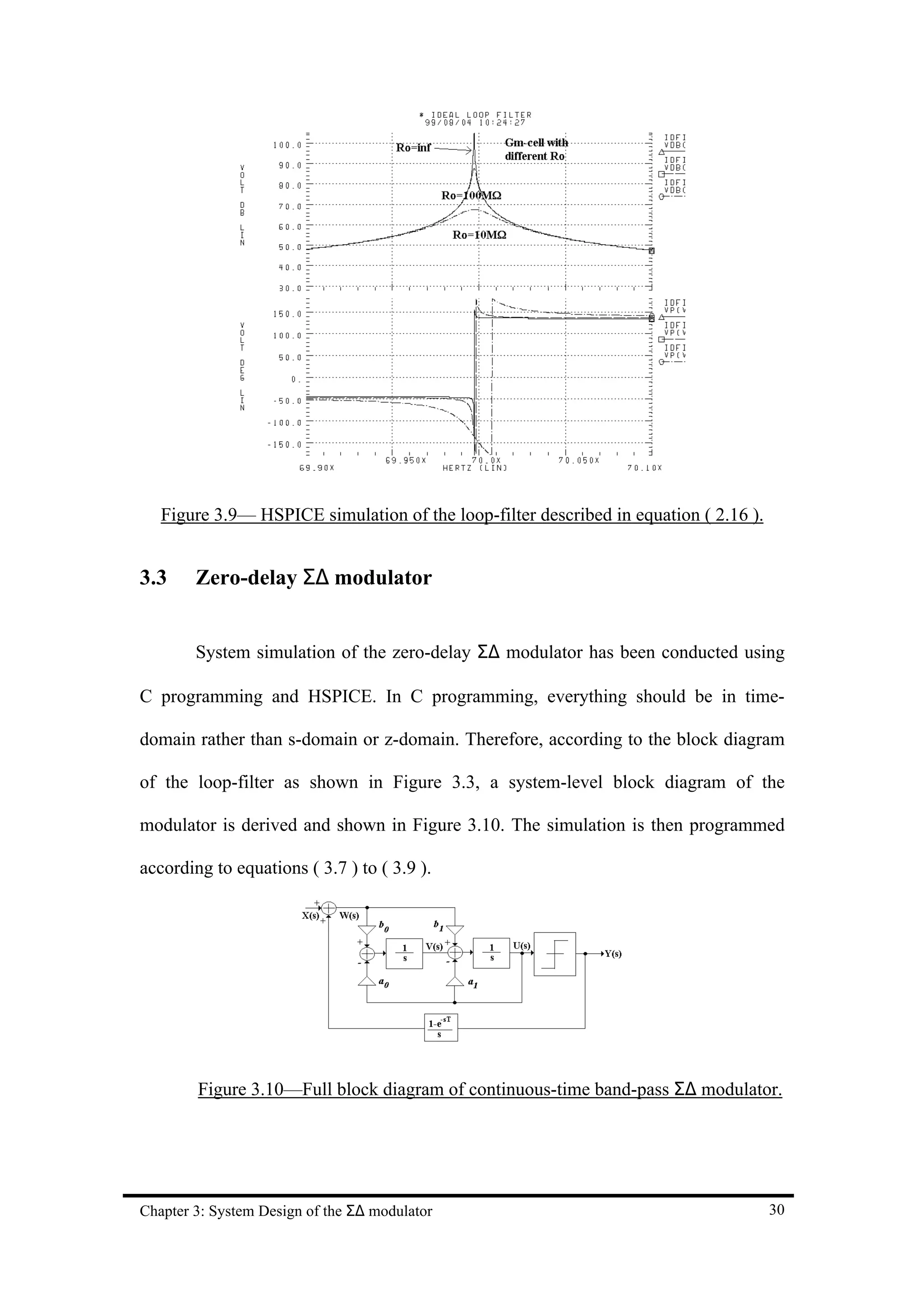
Figure 3.10—Full block diagram of continuous-time band-pass Σ∆ modulator. 30
Figure 3.11—C simulation of zero-delay Σ∆ modulator with infinite-Q loop-filter. 31
Figure 3.12—C simulation of the zero-delay Σ∆ modulator with loop-filter Q=50. 32
Figure 3.13—HSPICE ideal building block simulation of zero-delay Σ∆ modulator. 32
vi](https://image.slidesharecdn.com/sigmadeltaadc-130115093927-phpapp02/75/Sigma-delta-adc-8-2048.jpg)
![Chapter 2 Σ∆ fundamentals
2.1 Introduction [1],[2]
It is often desirable to convert analog signals into the digital domain using an
analog-to-digital converter (ADC). In this chapter the main properties of Σ∆
techniques that are useful for converting signals between analog and digital formats
are reviewed. Σ∆ modulation has become popular for achieving high resolution. A
significant advantage of the method is that analog signals are converted using not only
simple and high-tolerance analog circuits but also analog signal processing circuits
having a precision that is usually much less than the resolution of the overall
converter.
Conventional converters, as illustrated in Figure 2.1, are often difficult to
implement in fine-line VLSI technology with reasonably low power consumption.
These difficulties arise because conventional methods need analog components that
are precise and highly immune to noise and interference. However, the conversion
rate of conventional converters is Nyquist rate, i.e. sampling frequency is twice the
signal bandwidth. That is why conventional converters are usually referred to as
Nyquist converters.
Figure 2.1–Conventional Nyquist-rate ADC blocks [1].
Chapter 2: Σ∆ fundamentals 6](https://image.slidesharecdn.com/sigmadeltaadc-130115093927-phpapp02/75/Sigma-delta-adc-18-2048.jpg)
![The low-pass filter at the input to the encoder in Figure 2.1 attenuates high-
frequency noise and out-of-band signals to prevent them from aliasing into the desired
signal when sampled. The analog-to-digital circuit can take a number of different
forms such as flash converters for fast operation, successive-approximation converters
for moderate rates, and ramp converters for high resolution.
Oversampling converters can use simple and high-tolerance analog
components for implementation, but they require fast and complex DSP stages. The
use of high-frequency modulation can eliminate the need for abrupt cutoffs in the
analog anti-aliasing filters at the input to the ADCs. Σ∆ converters use the technique
of noise shaping in addition to oversampling to allow high-resolution conversion of
relatively low bandwidth signals.
This chapter is organized into five main sections. In Section 2.2, some basic
properties of the quantization noise are described. General oversampling ADC and Σ∆
modulator will be described in Section 2.3. Discrete-time low-pass Σ∆ modulation as
a technique for shaping the spectrum of quantization noise is introduced in Section
2.4. In Section 2.5 discrete-time band-pass Σ∆ modulation is explained, and in Section
2.6, the continuous-time design and implementation of band-pass Σ∆ modulator are
described.
2.2 Quantization noise [1],[2]
Quantization in amplitude and sampling in time are the two main functions of
all digital modulators. Once sampled, the signal samples must also be quantized in
amplitude to a finite set of output values. The typical transfer characteristic of
Chapter 2: Σ∆ fundamentals 7](https://image.slidesharecdn.com/sigmadeltaadc-130115093927-phpapp02/75/Sigma-delta-adc-19-2048.jpg)
![quantizers or ADCs with an input signal sample x and an output y is shown in Figure
2.2.
Figure 2.2–An example of a uniform multilevel quantization characteristic that is
represented by linear gain G and an error e [1].
The quantizer, embedded in any ADC is a non-linear system, is difficult to
analyze. To make the analysis tractable, it is useful to represent the quantized signal
y[n] by a linear function Gx[n] with an error e[n]: that is, y[n]=Gx[n]+e[n]. The gain
G is the slope of the straight line passing through the center of the quantization
characteristic. In Figure 2.2, the level spacing ∆ is 2. So, the quantizer does not get
saturated when -6≤x[n]≤6 and the error is bounded by ±∆/2. This consideration
remains applicable to a two-level (single-bit) quantizer but, in this case, the choice of
gain G is arbitrary.
To further simplify the analysis of the noise from the quantizer, the following
assumptions about the noise process and its statistics are traditionally made [3]:
1. The error sequence e[n] is a sample sequence of a stationary random process,
2. The error sequence is uncorrelated with the sequence x[n],
Chapter 2: Σ∆ fundamentals 8](https://image.slidesharecdn.com/sigmadeltaadc-130115093927-phpapp02/75/Sigma-delta-adc-20-2048.jpg)
![3. The random variables of the error process are uncorrelated; i.e. the error is a
white-noise process,
4. The probability distribution of the error process is uniform over the range of
quantization error.
For a zero mean e[n], its variance σe2 or power is:
∆
1 2 2 ∆2 ( 2.1 )
∆ ∫− 2
σe = e de =
2
∆
12
When a quantized signal is sampled at frequency fs=1/T, all of its power folds
into the frequency band 0≤f<fs. Then, if the quantization noise is white, the spectral
density of the sampled noise is given by:
σe
2
2 ( 2.2 )
E( f ) = =σe
fs fs
2
We can use this result to analyze oversampling modulators. Consider a signal
lying in the frequency band 0≤f≤fB. The oversampling ratio (OSR), defined as the
ratio of the sampling frequency fs to the Nyquist frequency 2fB, is given by the integer:
fs ( 2.3 )
OSR =
2 fB
Hence, the in-band quantization noise will be given by:
σ ( 2.4 )
2
2f
no = ∫
fB
E ( f )df = σ e ⋅ B = e
2 2 2
0 fs OSR
Chapter 2: Σ∆ fundamentals 9](https://image.slidesharecdn.com/sigmadeltaadc-130115093927-phpapp02/75/Sigma-delta-adc-21-2048.jpg)
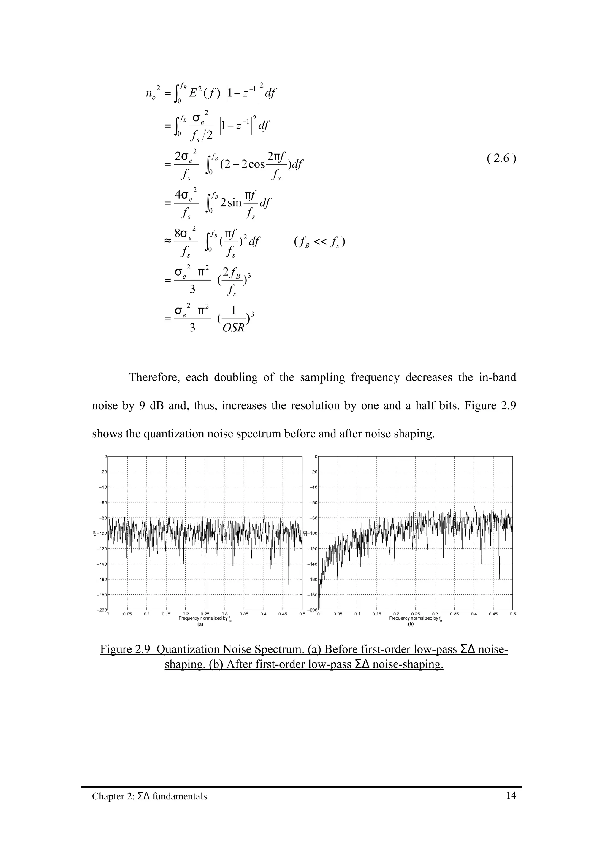
![Thus, we have the well-known result that oversampling reduces the in-band
quantization noise from ordinary quantization by the square root of the oversampling
ratio. Therefore, each doubling of the sampling frequency decreases the in-band noise
by 3 dB and thus increases the resolution by half a bit.
Figure 2.3 shows the power spectral density, E(f), of the quantization noise for
Nyquist rate sampling with rate fs1 and oversampling rate fs2. For Nyquist rate
sampling where the signal band, fB=fs1/2, all the quantization noise power, represented
by the area of the tall shaded rectangle, occurs across the signal bandwidth. In the
oversampled case, the same noise power, represented by the area of the unshaded
rectangle has been spread over a bandwidth equal to the sampling frequency, fs2,
which is much greater than the signal bandwidth, fB. Only a relatively small fraction
of the total noise power falls in the band [-fB,fB], and the noise power outside the
signal band can be greatly attenuated with a digital low-pass filter following the ADC.
Figure 2.3–Quantization noise power spectral density for Nyquist rate and
oversampled conversion [2].
2.3 Oversampling ADC and Σ∆ modulator [1],[2]
A general way of writing the discrete-time domain output of an ADC is given
as Y(z)=X(z)Hx(z)+E(z)He(z), where Hx is the signal transfer function (STF) and He is
Chapter 2: Σ∆ fundamentals 10](https://image.slidesharecdn.com/sigmadeltaadc-130115093927-phpapp02/75/Sigma-delta-adc-22-2048.jpg)
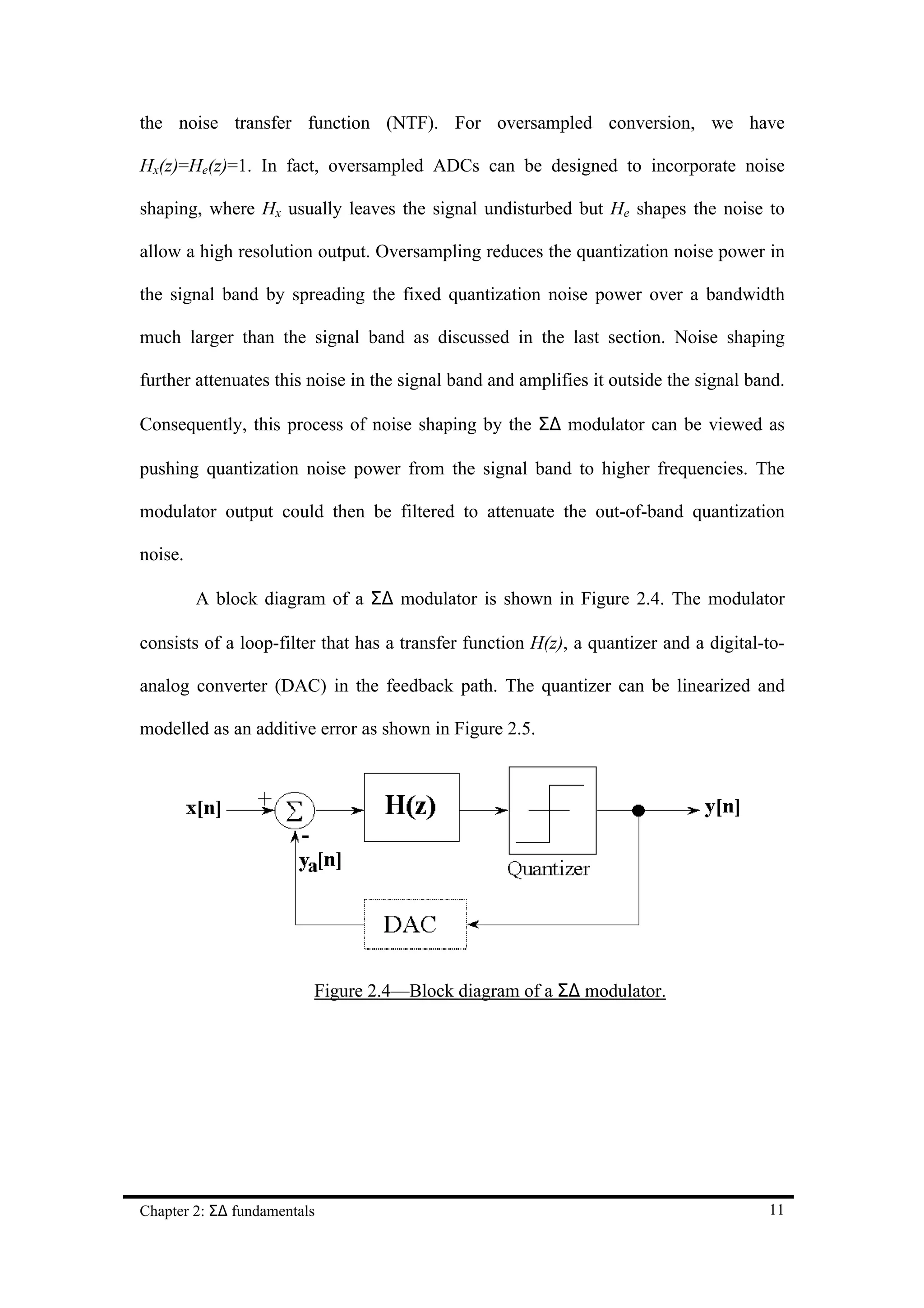
![Figure 2.5—Linearized model of the quantizer.
2.4 Discrete-Time Low-pass Σ∆ modulation [1],[2]
A block diagram of a first-order Σ∆ modulator is shown in Figure 2.6 and a
linearized version of the block diagram is shown in Figure 2.7.
Figure 2.6–Block diagram of a first-order Σ∆ modulator.
Figure 2.7—Linearized model block diagram of a first-order Σ∆ modulator.
The signal that is being quantized is a filtered version of the difference
between the input x[n] and an analog representation, ya[n], of the quantized output,
Chapter 2: Σ∆ fundamentals 12](https://image.slidesharecdn.com/sigmadeltaadc-130115093927-phpapp02/75/Sigma-delta-adc-24-2048.jpg)
![y[n]. The loop-filter is a discrete-time integrator whose transfer function is H(z) =
z-1/(1-z-1). If the DAC is ideal, it is replaced by a unity gain transfer function. The
modulator output Y(z) in the frequency domain is then given by:
Y ( z ) = X ( z ) ⋅ z −1 + E ( z ) ⋅ (1 − z −1 ) ( 2.5 )
so that the STF Hx(z) is z-1 and the NTF He(z) is 1-z-1. The output is just a delayed
version of the signal plus a quantization noise shaped by a first-order differentiator (or
high-pass filter). Note that a zero gain is provided by the NTF at DC frequency. The
magnitude spectrum of a first-order Σ∆ noise transfer function (NTF) is plotted in
Figure 2.8. The frequency axis has been normalized with respect to the sampling
frequency, fs.
Figure 2.8–First-order Noise Transfer Function (NTF) magnitude spectrum in dB.
The in-band quantization noise after the noise-shaping will be given by:
Chapter 2: Σ∆ fundamentals 13](https://image.slidesharecdn.com/sigmadeltaadc-130115093927-phpapp02/75/Sigma-delta-adc-25-2048.jpg)
![2.5 Discrete-Time Band-pass Σ∆ modulation [1],[2]
We have assumed that the sampling frequency, fs, is much greater than the
Nyquist rate. For low-pass signals, the highest frequency component is the signal
bandwidth fB. If a signal with a very narrow bandwidth fB is located at a center
frequency fc, its highest frequency component is then fc+fB/2. If fc is large, choosing a
fs much greater than the highest frequency would lead to an unreasonably large fs.
Band-pass Σ∆ modulation [4] allows high-resolution conversion of band-pass signals
if fs is much greater than the signal bandwidth fB, rather than the highest signal
frequency.
Unlike low-pass Σ∆ modulators that realize NTF zeros at DC or low
frequencies on the unit circuit of the Z plane, band-pass modulators have NTFs that
realize zeros or notches at the center frequency, fc, in the signal band of interest, [fc-
fB/2, fc+fB/2]. Consequently, quantization noise that occurs over the signal band is
attenuated, and noise power is pushed outside this band. No matter where the signal
band is centered, the smaller the signal bandwidth relative to the sampling frequency,
there is less in-band noise power for a given NTF. Noise outside the signal band can
then be attenuated with a digital decimation filter and, so, high-resolution conversion
is possible for large oversampling ratio fs/2fB.
Band-pass Σ∆ modulators operate in much the same manner as low-pass Σ∆
modulators. A band-pass Σ∆ modulator can be constructed by connecting a filter and
quantizer in a loop, as shown in Figure 2.10.
Chapter 2: Σ∆ fundamentals 15](https://image.slidesharecdn.com/sigmadeltaadc-130115093927-phpapp02/75/Sigma-delta-adc-27-2048.jpg)
![fc + f B 2
no = ∫
2
E 2 ( f ) ⋅ 1 + z −2 df
2
fc − f B 2
σe
2
fc + f B 2
=∫
2
⋅ 1 + z − 2 df
fc − f B 2 fs 2
2σ 4πf
2
fc + f B 2
= e ⋅∫ (2 + 2 cos )df
fs fc − f B 2 fs
fc + fB 2
4σ 4πf
2
f ( 2.8 )
= e ⋅ ( f + s sin )
fs 4π fs f
c − fB 2
4σ e 4πf c 4πf B
2
f
= ⋅{ f B + s [2 cos sin ]}
fs 4π fs 2 fs
4σ f 4πf B 2πf B
2
fs
= e ⋅ s ⋅[ − 2 sin ] ( fc = )
f s 4π fs fs 4
8σ e 2πf B 2πf B 1 2πf B 3
2
= ⋅[ − + ⋅( ) − ...]
4π fs fs 3! fs
σe ⋅ π2
2
1 3
≈ ⋅( )
3 OSR
Therefore, each doubling of the sampling frequency decreases the in-band
noise by 9 dB and, thus, increases the resolution by one and a half bits. Figure 2.13
shows the quantization noise spectrum before and after the second-order band-pass
Σ∆ noise shaping.
Figure 2.13–Quantization Noise Spectrum. (a) Before second-order band-pass Σ∆
noise-shaping, (b) After second-order band-pass Σ∆ noise-shaping.
Chapter 2: Σ∆ fundamentals 18](https://image.slidesharecdn.com/sigmadeltaadc-130115093927-phpapp02/75/Sigma-delta-adc-30-2048.jpg)
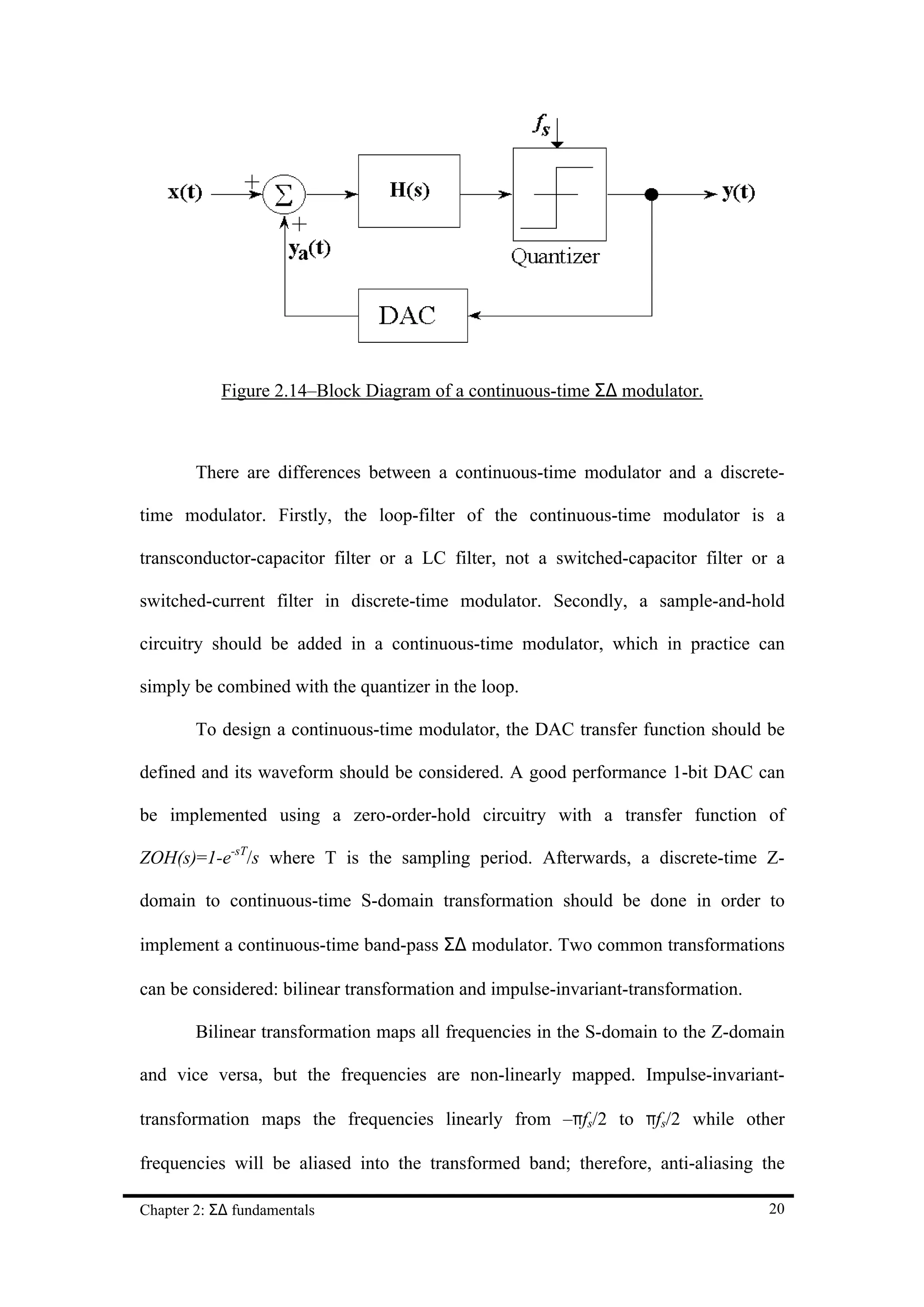
![2.6 Continuous-Time design and implementation of Band-pass Σ∆
modulator [5],[6],[7]
The discrete-time band-pass Σ∆ modulator eases the conversion of a band-pass
signal with a narrow bandwidth around the center frequency of the signal. However,
the switched-capacitor [8],[9],[10] or switched-current [11] implementation are
limited in that the sampling frequency of the modulators cannot be too high (usually
at under 100 MHz). Even using the double-sampling technique [12] or 2-path
technique [13],[14], the center frequency of the band-pass signal is still limited to
below 50 MHz. The modulator cannot operate at 70 MHz for high-IF conversion.
Therefore, a continuous-time design and implementation method for high-IF
conversion is worth investigating.
In a discrete-time system or switched-capacitor design, due to the discrete-
time nature of the modulator design, the DAC output waveform in the feedback loop
of the Σ∆ modulator does not have much effect on the modulator performance. The
variations of the digital-to-analog signal during the clock period φ and φ’ are not seen
by a switched-capacitor filter. However, a continuous-time filter responds to an input
signal continuously, unlike the switched-capacitor filter that is discrete in nature.
Therefore, a continuous-time Σ∆ loop-filter has to be designed according to the DAC
output waveform. Figure 2.14 shows the block diagram of a continuous-time Σ∆
modulator.
Chapter 2: Σ∆ fundamentals 19](https://image.slidesharecdn.com/sigmadeltaadc-130115093927-phpapp02/75/Sigma-delta-adc-31-2048.jpg)
![signal is important when using this transformation. There is a 70 MHz band-pass IF
filter before the modulator that served the anti-aliasing filter purpose in our proposed
receiver. Therefore, for design simplicity, the impulse-invariant-transformation was
chosen:
1 − e − sT ( 2.9 )
Z −1[ H ( z )] = L−1[ H ( s )]
s t = nT
where H(z) is the discrete-time transfer function of the loop-filter in the modulator,
H(s) is the continuous-time transfer function for the loop-filter, and 1-e-sT/s is the
transfer function of the DAC in the loop where T=1/fs.
For a continuous-time loop-filter, H(s) has the form of
N
ak ( 2.10 )
H ( s) = ∑
k =1 s − s k
Its impulse response is
N ( 2.11 )
h(t ) = ∑ a k e sk T u (t )
k =1
After the convolution with the DAC,
heq (t ) = ZOH * h(t )
+∞
= ∫−∞ ZOH ⋅ h(t − τ)dτ
∫0 h(t − τ)dτ
t
when 0 ≤ t < T
T
= ∫0 h(t − τ)dτ when t ≥ T
0 when t < 0
t N sk ( t −τ )
∫0 k∑1a k e dτ when 0 ≤ t < T
=
=
N
∫T ∑ ak e sk (t −τ) dτ when t ≥ T
k =1
0
Chapter 2: Σ∆ fundamentals 21](https://image.slidesharecdn.com/sigmadeltaadc-130115093927-phpapp02/75/Sigma-delta-adc-33-2048.jpg)
![Hence,
N ak sk t − sk t ( 2.12 )
k∑1− s e (e − 1) when 0 ≤ t < T
= k
heq (t ) =
∑ ak e sk t (e − skT − 1)
N
when t ≥ T
k =1− s k
Looking at samples of loop impulse response at sampling times t=nT,
0 when 0 ≤ t < T ( 2.13 )
N
heq (nT ) = a
∑ − sk e sk nT (e −skT − 1) when t ≥ T
k =1 k
The z-domain loop transfer function of the loop then can be derived from the
above equivalent impulse response:
+∞ +∞ N
a k sk nT − skT
H ( z) = ∑ h( n ) z − n = ∑ [ ∑
n = −∞ n =1 k =1 − sk
e (e − 1)]z − n
N +∞
a k − sk T
= ∑[ − 1)∑ (e skT z −1 ) n ]
( 2.14 )
(e
k =1 − sk n =1
N
ak z −1
=∑ (1 − e skT ) −1
where z k = e skT
k =1 − s k 1 − zk z
N ak ,eq z −1 ak
∴ H ( z) = ∑ −1
, a k ,eq = (1 − e skT )
k =1 1 − zk z − sk
From the above, a continuous-time loop-filter can be designed from a discrete-
time loop-filter:
π ( 2.15 )
−2 s−
z π 2T ]
H ( z) = H ( s) = − [
→
1 + z −2 4T s 2 + ( π ) 2
2T
where T is the sampling period of the modulator, i.e. T=1/fs.
Chapter 2: Σ∆ fundamentals 22](https://image.slidesharecdn.com/sigmadeltaadc-130115093927-phpapp02/75/Sigma-delta-adc-34-2048.jpg)
![Equation ( 2.15 ) assumes the loop delay for the Σ∆ modulator is zero.
However, in practical implementation, the quantizer is not delay-free. Therefore, if we
add more delay such that the total loop delay becomes exactly one sampling period T,
a digital delay z-1 is implemented in the loop. If we reserve this z-1 in the discrete-time
transfer function and implement the z-1 by digital delay cell,
π ( 2.16 )
s+
z −1 π 2T ]
H ( z) = H (s) =
→ [
1+ z −2
4T s 2 + ( π ) 2
2T
A continuous-time second-order band-pass Σ∆ modulator at 70 MHz can be
designed and implemented accordingly. The loop-filter can be implemented by a
transconductor-capacitor filter or a LC filter as mentioned above; the quantizer can be
implemented by a latched-type comparator; the ZOH circuit can be implemented by a
D flip-flop; the DAC can be implemented by a steering current source; and the
addition can be done using current addition.
In this project, both zero-delay and one-delay band-pass Σ∆ modulator are
implemented. As we will describe in the following chapters, a zero-delay modulator is
implemented using 0.8µm technology and source-degeneration Gm-cells while a one-
delay modulator is implemented using 0.5µm technology and triode-region Gm-cells.
Chapter 2: Σ∆ fundamentals 23](https://image.slidesharecdn.com/sigmadeltaadc-130115093927-phpapp02/75/Sigma-delta-adc-35-2048.jpg)
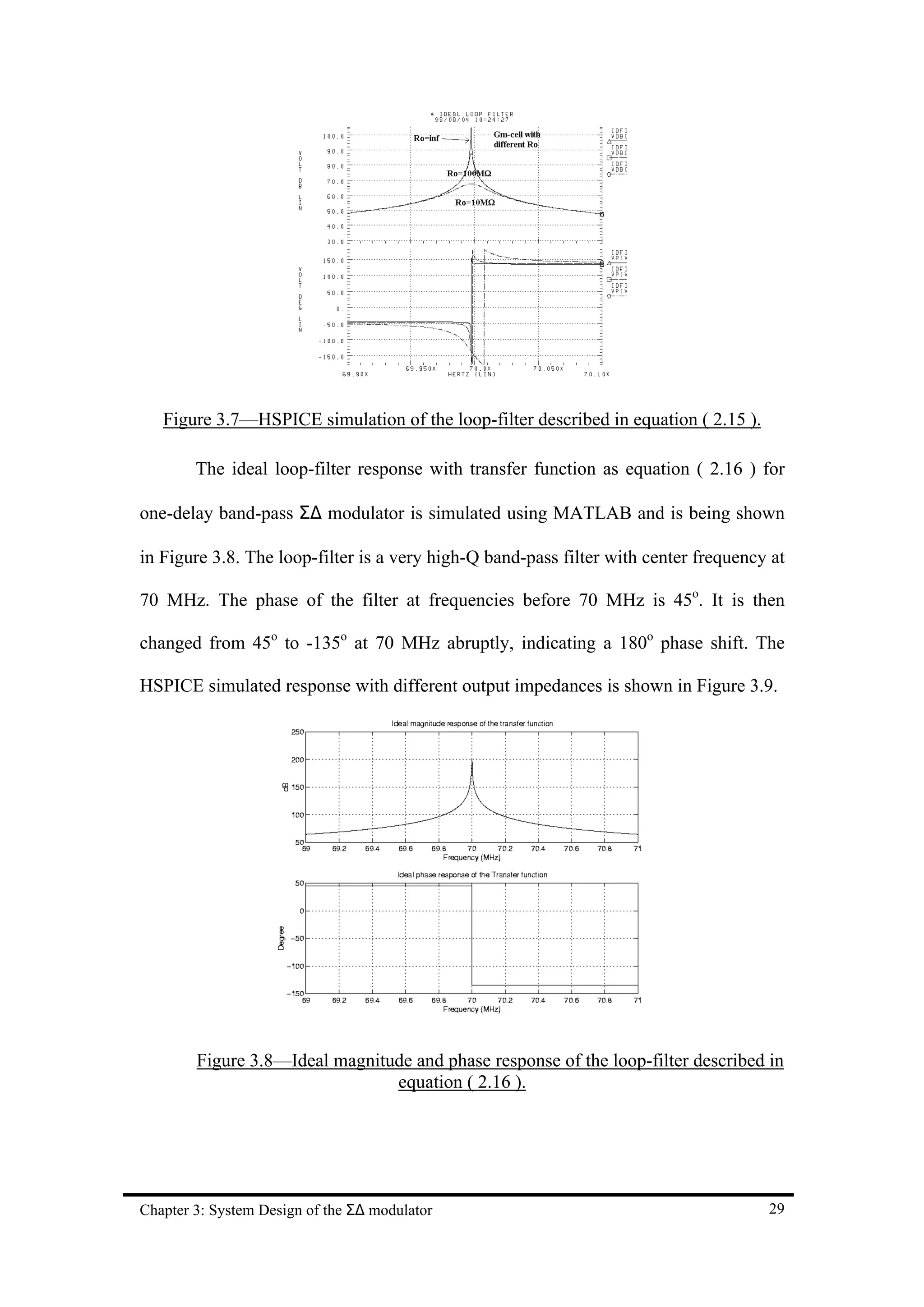
![70 MHz. The phase of the filter at frequencies before 70 MHz is –135o. It is then
changed from –135o to 45o at 70 MHz abruptly, indicating a 180o phase shift.
Figure 3.6—Ideal magnitude and phase response of the loop-filter described in
equation ( 2.15 ).
The ideal response of the loop-filter can never be achieved, however, as the
Gm-cells are not ideal. We assumed the Gm-cell has infinite output impedance. In
fact, every Gm-cell has finite output impedance. The transfer function implemented as
equation ( 3.5 ) will be changed as follows:
Gm3 Gm1 ⋅ Gm2 Gm3
s +[ + ]
Y (s) C2 C1 ⋅ C 2 ( R1 // R4 )C1C 2
H ( s) = =
X (s) 1 1 Gm2 ⋅ Gm4 1
s2 +[ + ]s + [− +
( R2 // R3 )C 2 ( R1 // R4 )C1 C1C 2 ( R2 // R3 )( R1 // R4 )C1C 2
( 3.6 )
where Rx is the output impedance of the x-th Gm-cell.
As shown in equation ( 3.6 ), if the output impedance of the Gm-cells is
infinite, equation ( 3.6 ) will then be simplified to equation ( 3.5 ). Using ideal
voltage-controlled-current-source (VCCS) in HSPICE with different output
impedances, the simulated magnitude and phase response is shown in Figure 3.7.
Chapter 3: System Design of the Σ∆ modulator 28](https://image.slidesharecdn.com/sigmadeltaadc-130115093927-phpapp02/75/Sigma-delta-adc-40-2048.jpg)
![^ ( 3.7 )
y (k ) = sign[u (k )] = sign[u (kT )]
^ ^ ^ ^ ( 3.8 )
u (k + 1) = u (kT ) + y (kT ) ⋅ T + b1 ∫kT +1)T x(t )dt + ∫kT +1)T v(t )dt
(k (k
^
− a1 ∫kT +1)T u (t )dt
(k
^ ^ ^ ( 3.9 )
v( M + 1) = v( MTo ) − ao u ( MTo ) ⋅ ∆t + bo ∫MTo+1)To x(t )dt
(M
^
+ y (t ) ⋅ To
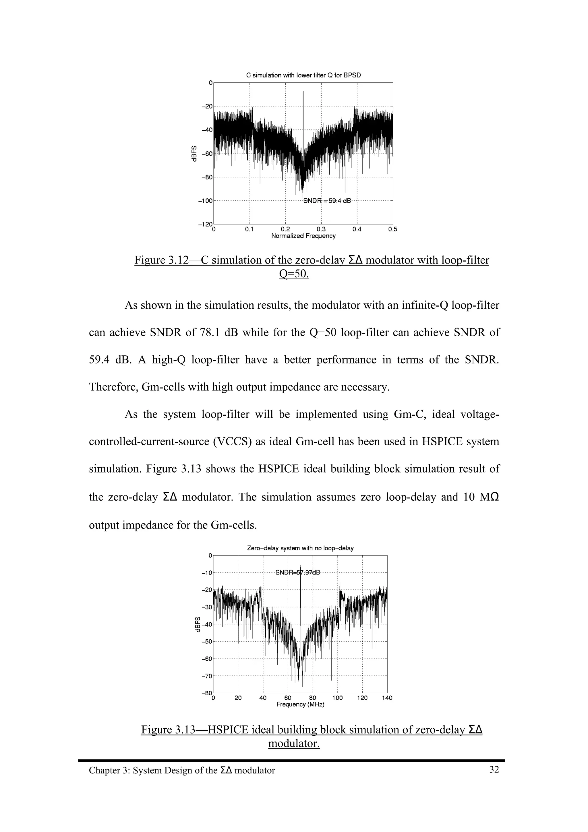
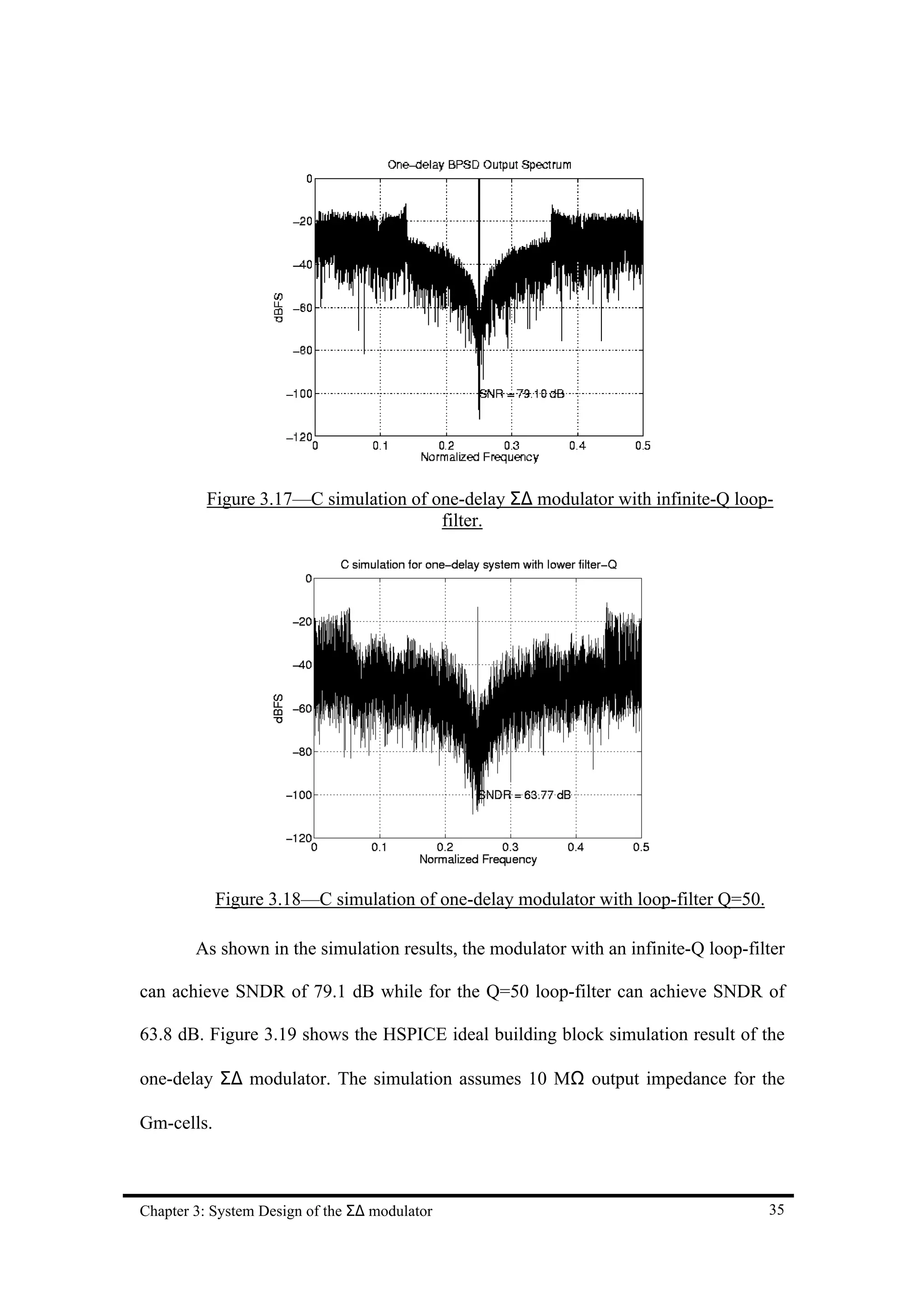
Figure 3.11 shows the C simulation result of the zero-delay Σ∆ modulator. The
simulation assumes the loop-filter has an infinite Q and zero loop-delay. Another C
simulation assuming the loop-filter has a finite Q of 50 and zero loop-delay has
performed and the simulation result is shown in Figure 3.12.
Figure 3.11—C simulation of zero-delay Σ∆ modulator with infinite-Q loop-
filter.
Chapter 3: System Design of the Σ∆ modulator 31](https://image.slidesharecdn.com/sigmadeltaadc-130115093927-phpapp02/75/Sigma-delta-adc-43-2048.jpg)
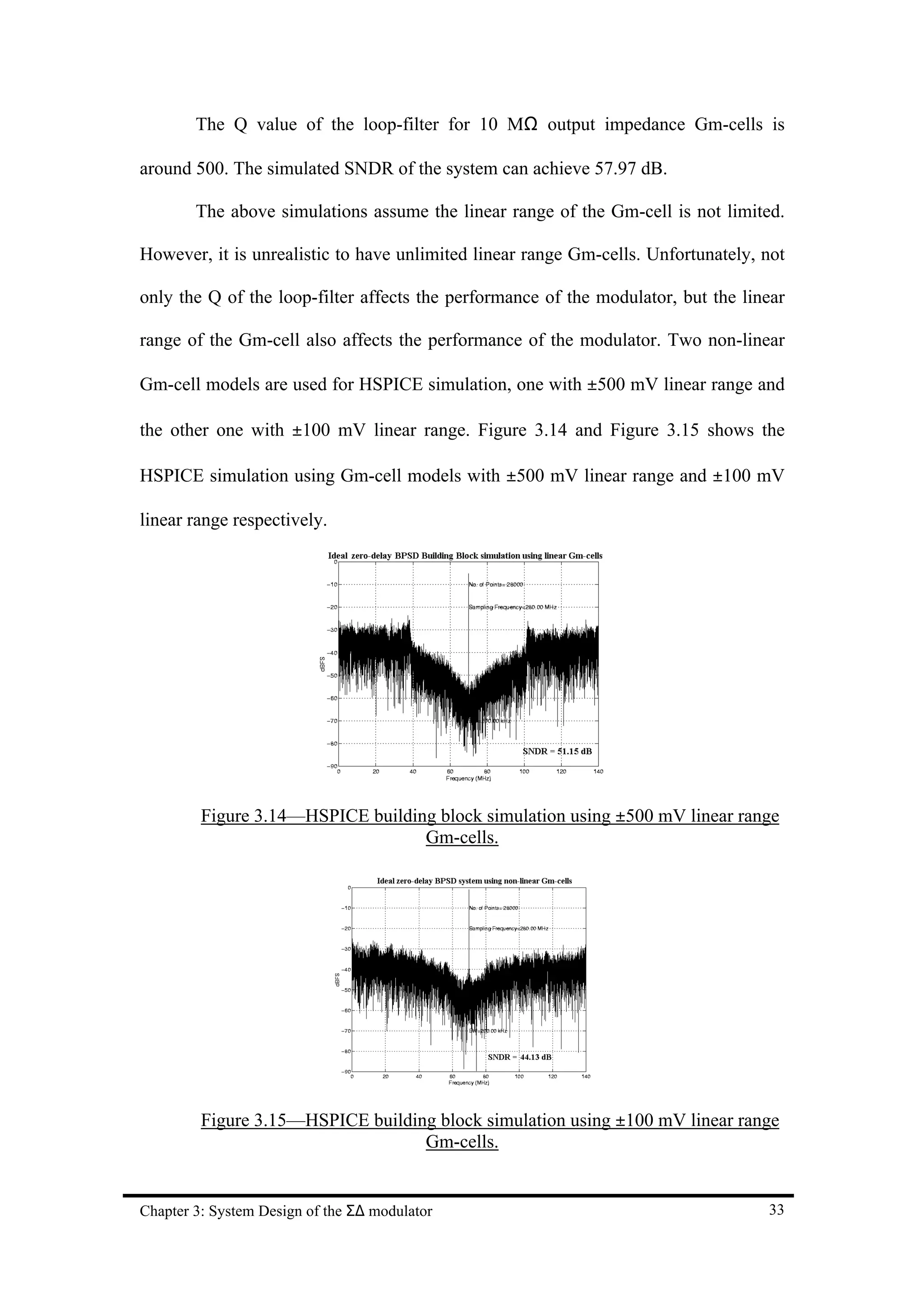
![The modulator with ±500 mV linear range Gm-cells can achieve 51.2 dB of
SNDR while the one with ±100mV linear range Gm-cells can achieve 44.1 dB only.
Therefore, Gm-cells with large linear range are needed for a high-performance
modulator.
In all the simulations shown above, loop-delay of the system is assumed to be
zero. In practice, the loop-delay of the system cannot be zero. Figure 3.16 shows the
simulation result when the loop-delay of the modulator is 2.6 ns. The loop-delay
degrades the SNDR performance of the modulator [7]. The simulated SNDR is 44.84
dB. Since loop-delay is unavoidable in the modulator, it is better to make the loop-
delay to be exactly equal to one sampling period in order to change the design to one-
delay modulator.
Figure 3.16—HSPICE ideal building block simulation for zero-delay Σ∆
modulator with 2.6 ns loop-delay.
3.4 One-delay Σ∆ modulator
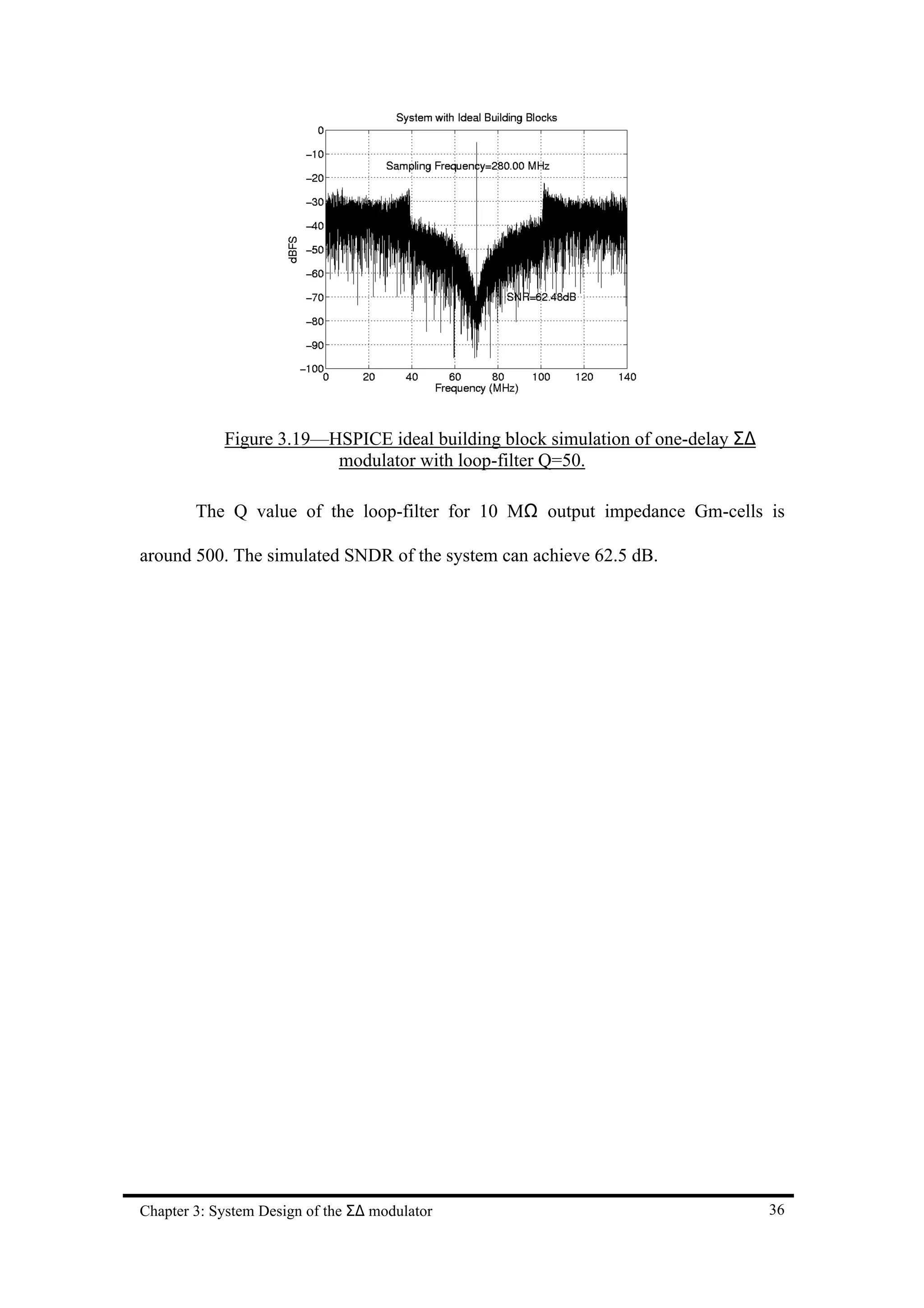
Figure 3.17 shows the C simulation result of the zero-delay Σ∆ modulator. The
simulation assumes the loop-filter has an infinite Q and zero loop-delay. Another C
simulation assuming the loop-filter has a finite Q of 50 and zero loop-delay has
performed and the simulation result is shown in Figure 3.18.
Chapter 3: System Design of the Σ∆ modulator 34](https://image.slidesharecdn.com/sigmadeltaadc-130115093927-phpapp02/75/Sigma-delta-adc-46-2048.jpg)
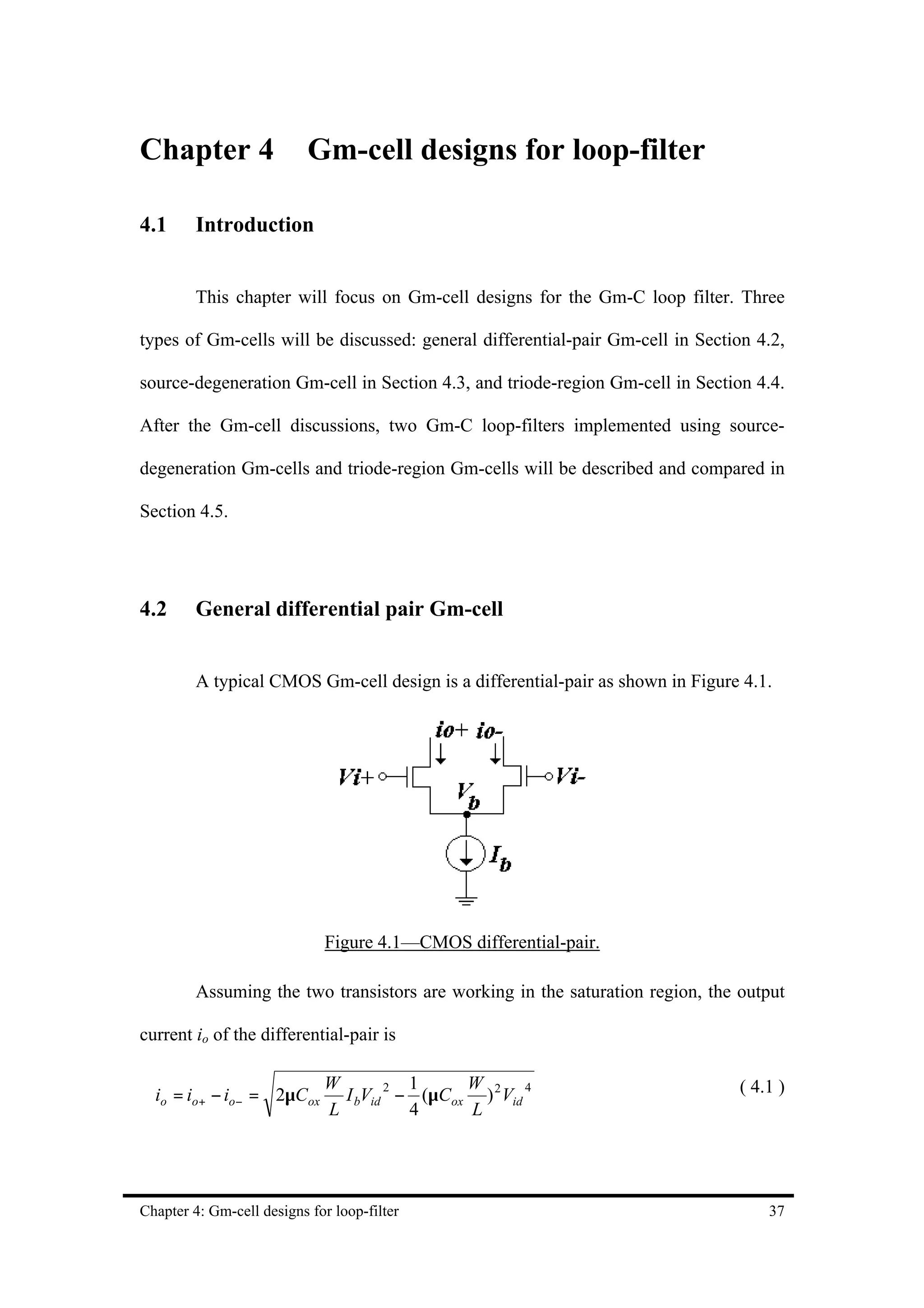
![The Gm of the differential-pair is then
∂io
Gm = ( 4.2 )
∂Vid
3
W
3( µC ox ) 2
W L V 2 + ...
= 2 µC ox I b − id
L 4 2I b
From equation ( 4.2 ), for small input signals, the Gm is constant. However,
for large input signals, Gm drops and becomes non-linear. As a result, techniques for
linearizing Gm-cells are needed to be used.
4.3 Source-degeneration Gm-cell
The first way to design a linear Gm-cell is source degeneration [17] as shown
in Figure 4.2.
Figure 4.2—Source-degeneration CMOS differential-pair.
Gm of the degenerated differential-pair is
gm ( 4.3 )
Gm =
1 + gm ⋅ R
where gm is the transconductance of a single transistor. When gmR is much larger
than 1, the Gm of the degenerated-differential-pair can be approximated as 1/R.
Chapter 4: Gm-cell designs for loop-filter 38](https://image.slidesharecdn.com/sigmadeltaadc-130115093927-phpapp02/75/Sigma-delta-adc-50-2048.jpg)
![However, it is unrealistic for a very large value of R to be implemented
monolithically. Therefore, triode region transistor is used to implement the
degeneration resistor R. The resistance of a triode region transistor is:
1 ( 4.4 )
R=
W
µCox (Vgs − Vt − Vds )
L
A source-degeneration Gm-cell using 0.8µm technology has been designed.
The circuit schematic is shown in Figure 4.3.
Figure 4.3—Designed source-degeneration Gm-cell.
It is desired to have very high output impedance, in the order of tens of MΩ,
for Gm-cells for high-Q filters. However, it is difficult to obtain. For the design as
shown in Figure 4.3, the output impedance is in the order of tens of kΩ, therefore, a
Q-tuning circuitry is needed to enhance the Q-value of the filter by increasing the
output impedance of the Gm-cell. A usual technique called negative-impedance-
compensation (NIC) [15] technique is used in Gm-C filter to increase the output
impedance of the Gm-cell. The source-degeneration Gm-cell with the NIC circuit is
shown in Figure 4.4. The transistors Mqb, Mq1 and Mq2 formed a negative-Gm-cell.
Chapter 4: Gm-cell designs for loop-filter 39](https://image.slidesharecdn.com/sigmadeltaadc-130115093927-phpapp02/75/Sigma-delta-adc-51-2048.jpg)
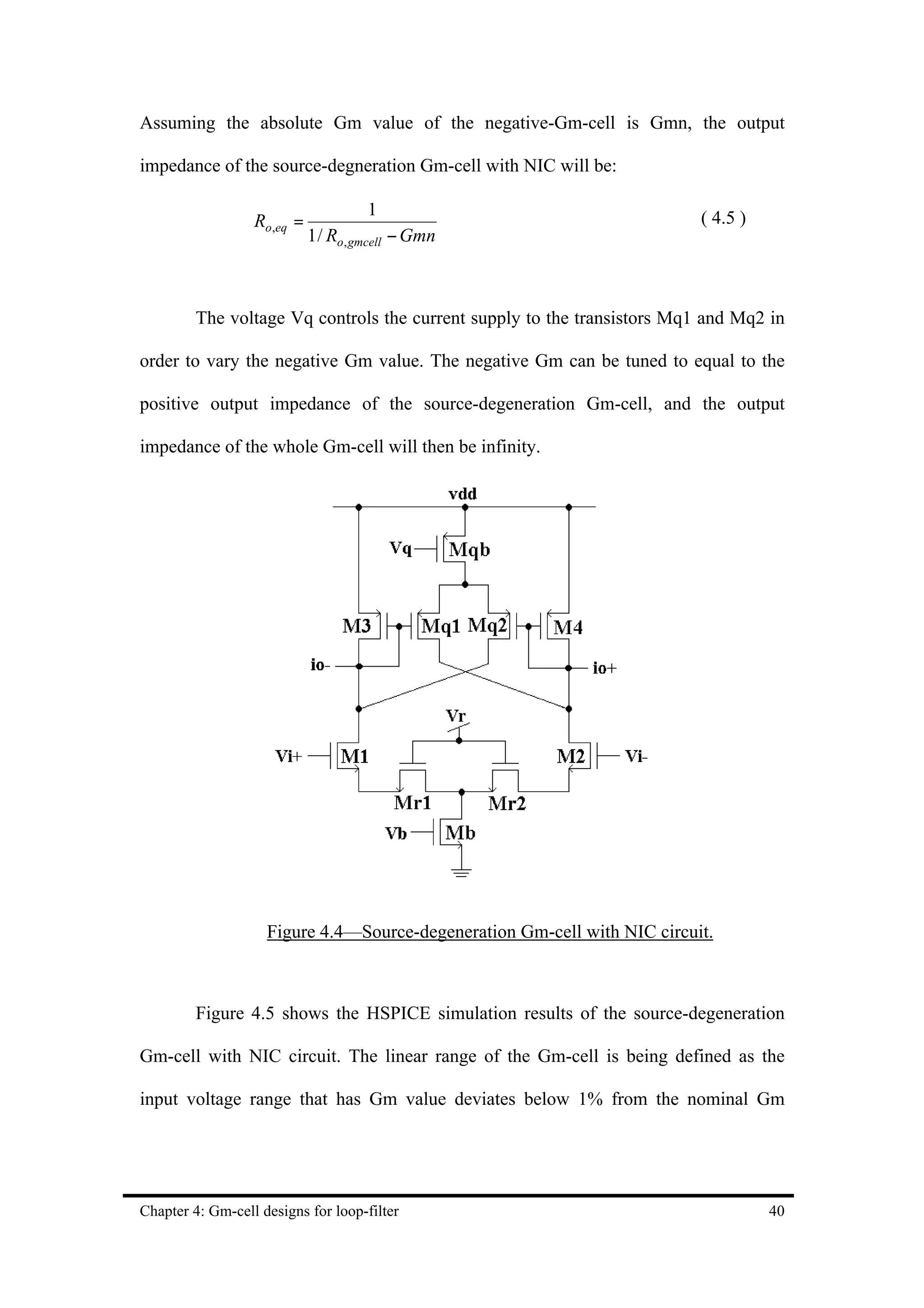
![value. The linear range of this Gm-cell is around ±90mV with 3 V power supply. The
current supply to the Gm-cell is 0.75 mA.
Figure 4.5—HSPICE simulation result of the source-degeneration Gm-cell.
4.4 Triode-region Gm-cell
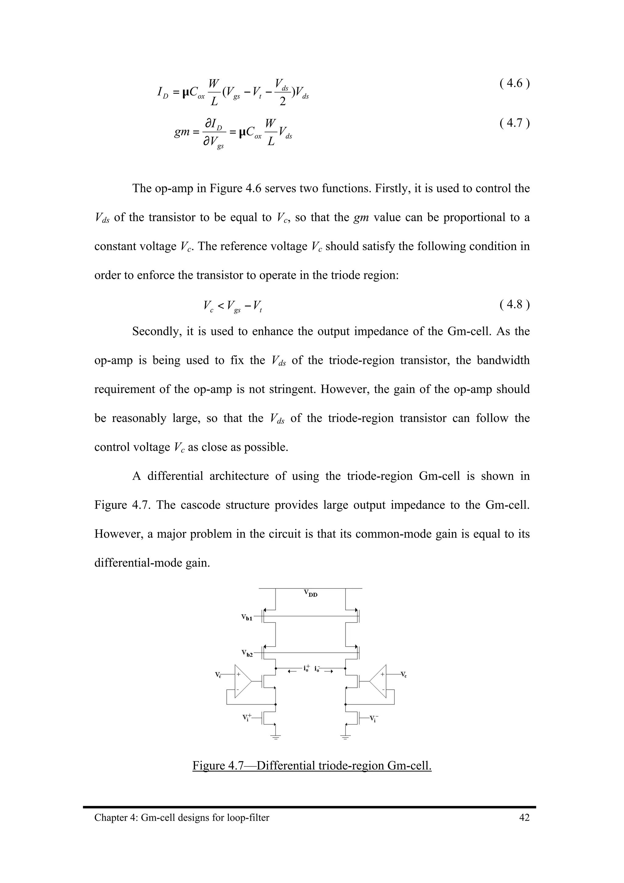
Another method of designing a linear Gm-cell is to use a triode-region
transistor [7],[16] as shown in Figure 4.6. The current of a triode-region transistor is
shown in equation ( 4.6 ) and the transconductance gm is shown in equation ( 4.7 ).
Figure 4.6—Triode-region Gm-cell.
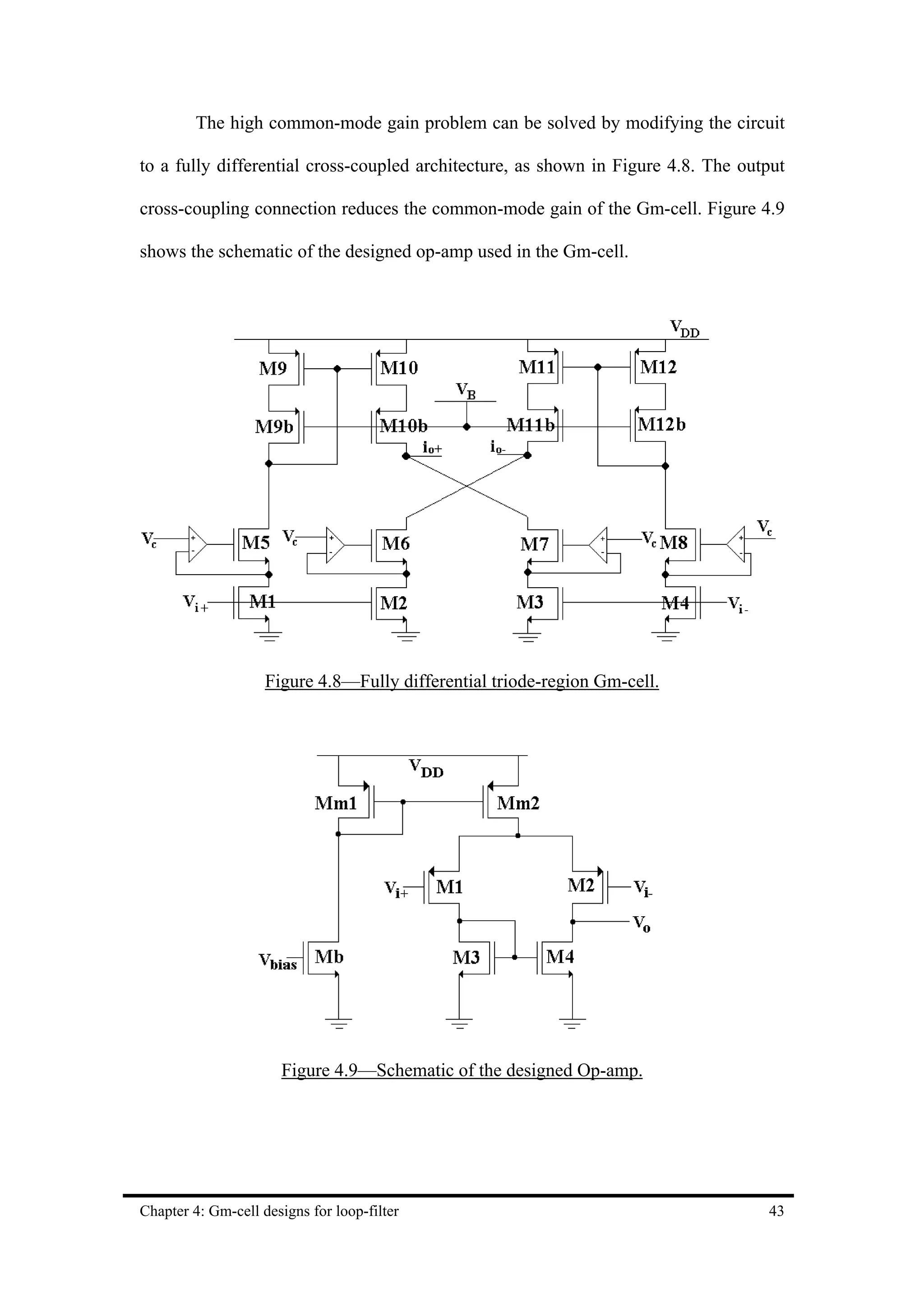
Chapter 4: Gm-cell designs for loop-filter 41](https://image.slidesharecdn.com/sigmadeltaadc-130115093927-phpapp02/75/Sigma-delta-adc-53-2048.jpg)
![Chapter 5 Quantizer Design
5.1 Introduction
A core component of any analog-to-digital converter (ADC) is a quantizer. As
mentioned in Chapter 2, Nyquist converters need precise analog components in their
conversion circuits. Typically, a quantizer design includes a very precise sample-and-
hold circuit and a high-accuracy comparator working at Nyquist sampling frequency.
The accuracy requirement of the comparator depends on the accuracy requirement of
the converter, e.g. an 8-bit ADC requires a comparator with at least 8-bit accuracy. In
contrast, in Σ∆ modulators, the comparator is required to work at a high oversampling
frequency but its resolution can be as small as 1 bit. Therefore, the comparator design
in Σ∆ modulators focuses more on a high-speed operation instead of accuracy.
In Section 5.2, a latched-type comparator for the quantizer design will be
described. As mentioned in Chapter 2, the quantized signal should be a non-return-to-
zero (NRZ) waveform, therefore a zero-order-hold (ZOH) circuit is needed. In
Section 5.3, a true-single-phase-clock (TSPC) D flip-flop for the ZOH circuit will be
described. Finally, a simple feedback DAC design and the HSPICE simulation of the
whole quantizer will be shown in Sections 5.4 and 5.6 respectively.
5.2 Comparator Design
To combine the sample-and-hold function and the comparator function in a
quantizer, the latched-type comparator [18],[19] is the best choice. Figure 5.1 depicts
Chapter 5: Quantizer Design 49](https://image.slidesharecdn.com/sigmadeltaadc-130115093927-phpapp02/75/Sigma-delta-adc-61-2048.jpg)
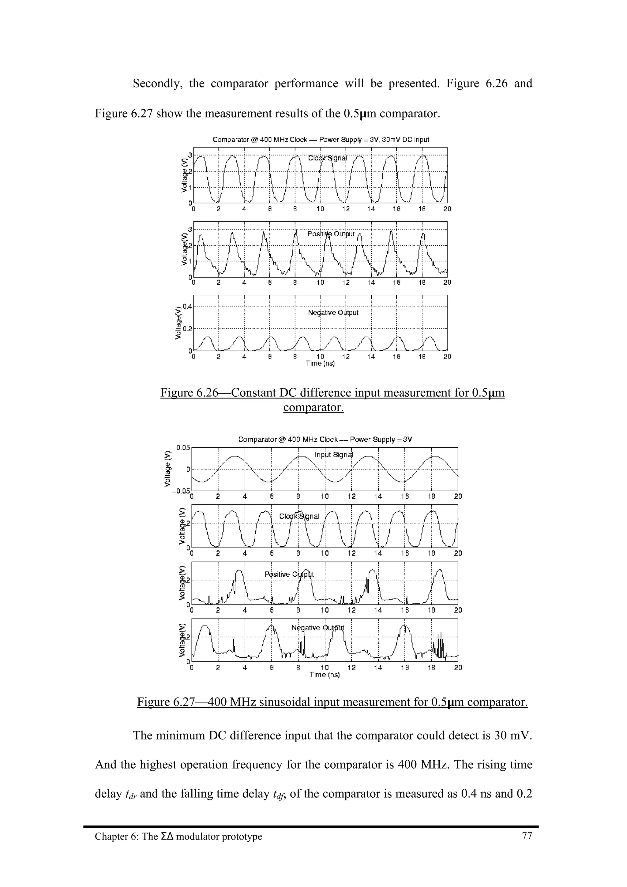
![For the design using 0.8µm technology, the rising time delay, tdr, from the
clock to the output is 0.95ns. The falling time delay, tdf, from the clock to the output is
0.53ns. The rising time, tr, of the output is 0.73ns and the falling time, tf, of the output
is 0.28ns. The total current supply of the comparator is 3 mA at operation frequency
of 280 MHz and 3 V power supply.
For the design using 0.5µm technology, the rising time delay, tdr, from the
clock to the output is 0.83ns. The falling time delay, tdf, from the clock to the output is
0.27ns. The rising time, tr, of the output is 0.62ns and the falling time, tf, of the output
is 0.15ns. The total current supply of the comparator is 2.6 mA at operation frequency
of 280 MHz and 3 V power supply. Table 5.2 shows the summary of the simulated
results of two designed latched-type comparators.
0.8µm 0.5µm
Operation frequency 320 MHz 320 MHz
Rising time delay 0.95 ns 0.83 ns
Falling time delay 0.53 ns 0.27 ns
Rising time 0.73 ns 0.62 ns
Falling time 0.28 ns 0.15 ns
Current supply at 3 V at 280 MHz 3 mA 2.6 mA
Table 5.2—Summary of simulated results of the latched-type comparators.
5.3 D flip-flop Design
In order to convert the return-to-zero (RZ) output of the comparator to a NRZ
output, a D flip-flop is added after the latched-type comparator. It is too slow for
usual static D flip-flop to be used in a 280 MHz sampling system, therefore, a TSPC
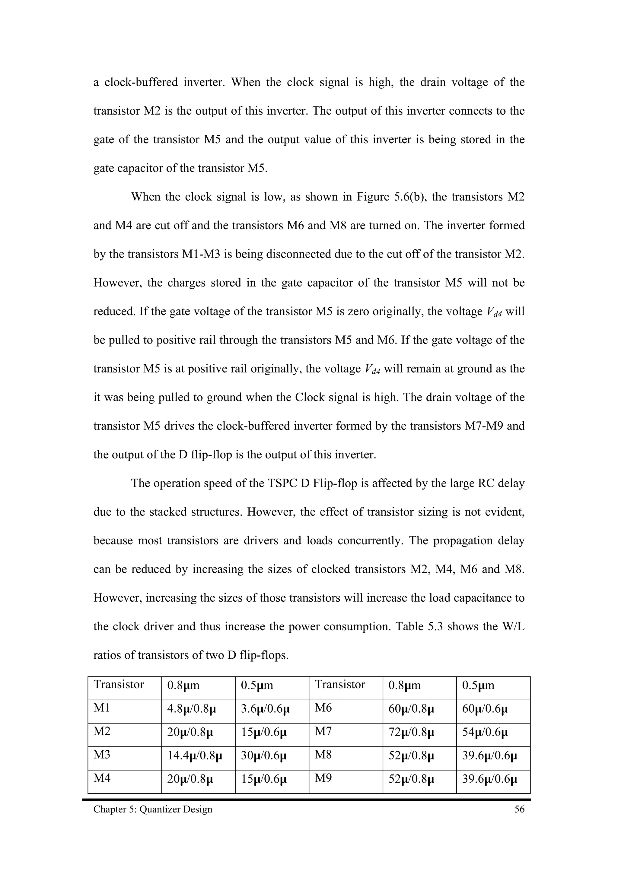
D flip-flop [20],[21] is chosen. Figure 5.5 shows the schematic of the design of the
Chapter 5: Quantizer Design 54](https://image.slidesharecdn.com/sigmadeltaadc-130115093927-phpapp02/75/Sigma-delta-adc-66-2048.jpg)
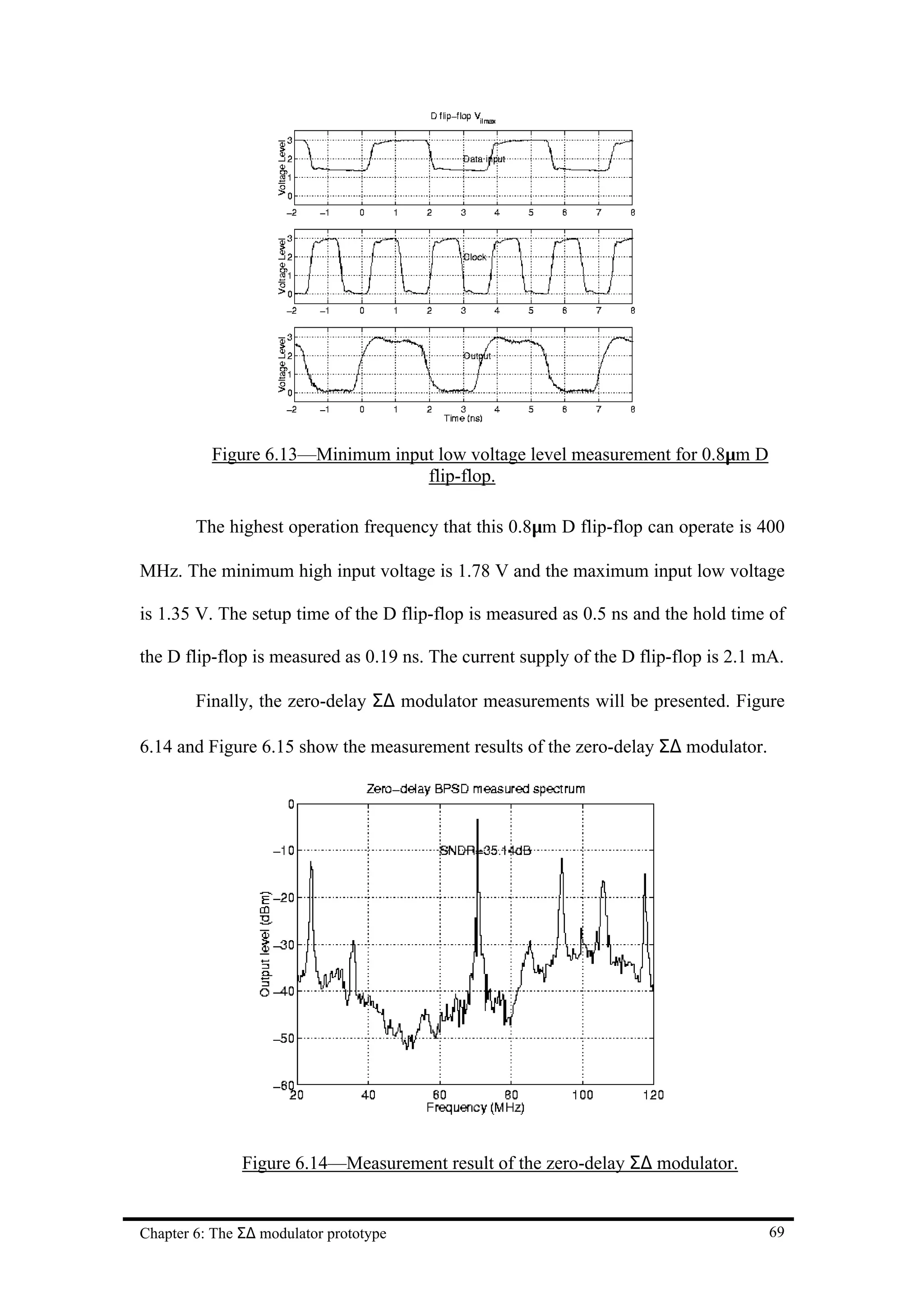
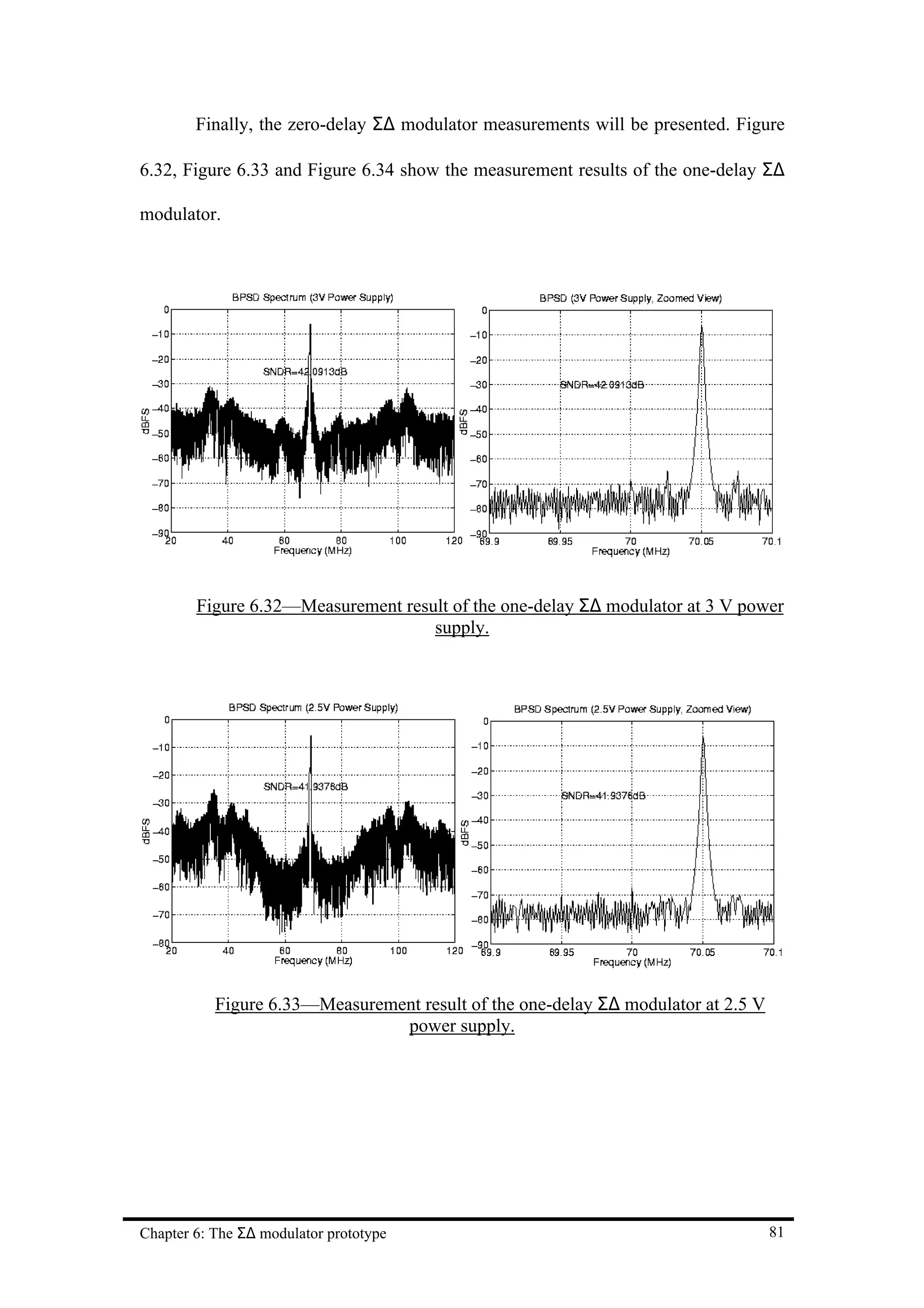
![Chapter 7 Conclusion
7.1 Conclusion
Two 70 MHz second-order continuous-time band-pass Σ∆ modulators have
been fabricated and tested using 0.8µm and 0.5µm CMOS technology. They show out
a high-speed data conversion at IF equals to 70 MHz. The current supply to the circuit
is small implies the power consumption of the circuit is small also. Measured SNDR
for 0.8µm design is 35.14 dB (5.9 bits of resolution) and for 0.5µm design is 42.09 dB
(7 bits of resolution). However, there are some problems in the circuit.
The problem of the 0.8µm design are the non-symmetrical noise-shape and the
low measured SNDR. The problems are due to the following reasons:
• insufficient linear range of the Gm-cell, and
• excess loop-delay in zero-delay modulator design.
Design fB IF SNDR Power Vdd # of orders Process
th
1 [24] 200 kHz 100 MHz 45 dB 330 mW 2.7/3.3 V 4 -order 0.5µm CMOS
2 [25] 200 kHz 950 MHz 49 dB 135 mW 5V 2nd-order 0.5µm Bipolar
3 [12] 2 MHz 40 MHz 45 dB 65 mW 3.3 V 4th-order 0.5µm CMOS
My 200 kHz 70 MHz 42 dB 47 mW 3V 2nd-order 0.5µm CMOS
design 41.9 dB 35 mW 2.5 V
Table 7.1—Σ∆ modulators performance comparison.
Table 7.1 shows a performance comparison between different designs and my
design. As not much work on 70 MHz modulator has been reported, a direct
comparison cannot be made. However, we can still compare the performances of
different modulators correspondingly.
Chapter 7: Conclusion 84](https://image.slidesharecdn.com/sigmadeltaadc-130115093927-phpapp02/75/Sigma-delta-adc-96-2048.jpg)
![References
[1] S. R. Norsworthy, R. Schreier & G. C. Temes, “Delta-Sigma Data Converters:
Theory, Design, and Simulation”, IEEE Press, 1998.
[2] P. M. Aziz, H. V. Sorensen, & J. V. Spiegel, “An Overview of Sigma-Delta
Converters”, IEEE Signal Processing Magazine, pp.61-84, Jan. 1996.
[3] A. Oppenheim & R. Schafer, “Discrete Time Signal Processing”, Prentice-Hall,
1989.
[4] R. Schreier & M. Snelgrove, “Band-pass Sigma-Delta modulation”, Electronics
Letters, pp.1560-1561, Feb. 1991.
[5] O. Shoaei & W. M. Snelgrove, “Optimal (bandpass) Continuous-time Σ∆
modulator”, Proceedings of IEEE International Symp. on Circuits & Systems,
vol. 5, pp.489-492, 1994.
[6] O. Shoaei & W. M. Snelgrove, “Design & Implementation of a Tunable 40 MHz
– 70 MHz Gm-C Bandpass ∆Σ Modulator”, IEEE Trans. on Circuits & Systems
II, vol. 44, no. 7, pp.521-530, July 1997.
[7] O. Shoaei, “Continuous-time Delta-Sigma A/D Converters for high-speed
applications”, Ph.D. dissertation, Carleton Univ., Ottawa, Ont., Canada, Feb.
1996.
[8] S. Jantzi, R. Schreier & M. Snelgrove, “Band-pass Sigma-Delta Analog-to-
Digital Conversion”, IEEE Trans. on Circuits & Systems, vol. 38, no. 11,
pp.1406-1409, Nov. 1991.
[9] F. W. Singor & W. M. Snelgrove, “Switched-Capacitor Band-pass Delta-Sigma
A/D Modulation at 10.7 MHz”, IEEE J. of Solid-State Circuits, vol. 30, no. 3,
pp.184-192, March 1995.
[10] S. A. Jantzi, W. M. Snelgrove & P. F. Ferguson, “A Fourth-order Bandpass
Sigma-Delta Modulator”, IEEE J. of Solid-State Circuits, vol. 28, no. 3, pp.282-
291, March 1993.
[11] L. Luh, J. Choma & J. Draper, “A 50-MHz Continuous-time switched-current
Σ∆ modulator”, Proceedings of IEEE International Symp. on Circuits &
Systems, June 1998.
References 86](https://image.slidesharecdn.com/sigmadeltaadc-130115093927-phpapp02/75/Sigma-delta-adc-98-2048.jpg)
![[12] S. Bazarjani & M. Snelgrove, “A 40 MHz IF Fourth-order Double-Sampled SC
Bandpass Σ∆ Modulator”, Proceedings of IEEE International Symp. on Circuits
& Systems, June 1997.
[13] A. K. Ong & B. A. Wooley, “A two-path bandpass Sigma Delta modulator for
digital IF extraction at 20 MHz”, IEEE International Solid-State Circuit
Conferecne 1997, Feb. 1997.
[14] A. K. Ong & B. A. Wooley, “A two-path bandpass Sigma Delta modulator for
digital IF extraction at 20 MHz”, IEEE J. of Solid-State Circuits, vol. 32, no. 12,
pp.1920-34, Dec. 1997.
[15] J. E. Kardontchik, “Introduction to the design of Transconductor-Capacitor
Filters”, Kluwer Academic Publishers, 1992.
[16] D. A. Johns & K. Martin, “Analog Integrated Circuit Design”, Wiley, 1997.
[17] P. R. Gray & R. G. Meyer, “Analysis & Design of Analog Integrated Circuits”,
3rd. Ed., Wiley, 1993.
[18] A. Yukawa, “A CMOS 8-bit high-speed A/D converter IC”, IEEE J. of Solid-
State Circuits, vol. no. SC-20, no. 3, June 1985.
[19] J. Ho & H. Luong, “A 3-V 1.47mW 120-MHz Comparator for Use in Pipeline
ADC”, Proceedings of IEEE Asia-Pacific Conference on Circuits and Systems
96, pp. 413-416, Nov. 1996.
[20] J. Yuan & C. Svensson, “High-speed CMOS circuit technique”, IEEE J. of
Solid-State Circuits, vol. 24, no. 2, pp.62-70, 1989.
[21] B. Chang, J. Park & W. Kin, “A 1.2 GHz CMOS Dual-Modulus Prescaler Using
New Dynamic D-Type Flip-Flops”, IEEE J. of Solid-State Circuits, vol. 31, no.
5, pp. 749-752, May 1996.
[22] R. M. Gray, “Oversampled Σ∆ modulation”, IEEE Trans. on Communication,
vol. COM-35, pp.481-489, Apr. 1987.
[23] R. M. Gray, “Quantization noise spectra”, IEEE Trans. on Information Theory,
vol. IT-36, pp.1220-44, Nov. 1990.
[24] H. Tao & J. M. Khoury, “A 100 MHz IF, 400 MSamples/s CMOS Direct-
Conversion Bandpass Σ∆ Modulator”, IEEE International Solid-State Circuit
Conferecne 1999, Feb. 1999.
References 87](https://image.slidesharecdn.com/sigmadeltaadc-130115093927-phpapp02/75/Sigma-delta-adc-99-2048.jpg)
![[25] W. Gao & W. M. Snelgrove, “A 950 MHz IF Second-Order Integrated LC
Bandpass Delta-Sigma Modulator”, IEEE J. of Solid-State Circuits, vol. 33, no.
5, May 1998.
References 88](https://image.slidesharecdn.com/sigmadeltaadc-130115093927-phpapp02/75/Sigma-delta-adc-100-2048.jpg)