SlideShare a Scribd company logo
1 of 85
Download to read offline
Chapter-8: Introduction to Second-Order Circuits
8.1 Introduction
• In the chapter-7 we considered circuits with a single energy storage
element (ESE) i.e. either a capacitor or an inductor.
• Such circuits are called first-order circuits, because the differential
equations describing them are of first-order.
• Now in this chapter we consider circuits with two ESEs, known as
second-order circuits because their responses are described by
differential equations that contain second derivatives.
• Typical examples of second-order circuits are RLC circuits, in which
the three kinds of passive elements are present.
• Examples of such circuits are shown in Fig. 8.1(a) and (b).
• Other examples are RL & RC circuits, shown
in Fig. 8.1(c) and (d).
• It is apparent from Fig. 8.1 that a second-
order circuit may have two storage elements
of different type or the same type.
• Usually two storage elements appear in circuit
when elements of the same type cannot be
represented by an equivalent single element.
• Op amp circuit with two storage elements is
also a 2nd-order circuit.
• As with first-order circuits, a second-order
circuit may contain several resistors and
dependent and independent sources.
• A second-order circuit is characterized by a second-order differential
equation and consists of resistors plus equivalent of two ESEs.
• Analysis of second-order circuits is similar to first-order circuits.
• We will first consider circuits that are excited by the initial conditions
of the storage elements.
• Although such circuits may contain dependent sources, they are free
of independent sources.
• These source-free circuits will give natural responses as expected.
• Later we will consider circuits excited by independent sources.
• Such circuits yield both the transient and the steady-state response.
• We consider only DC independent sources in this chapter.
• Case of sinusoidal & exponential sources is deferred to later chapters.
• We begin by learning how to obtain the initial conditions for the
circuit variables and their derivatives.
• Then we consider series and parallel RLC circuits for the two cases of
excitation: i.e. by initial conditions of the ESEs and by step inputs.
• Later we will examine some other types of second-order circuits.
Finding Initial and Final Values
• Major problem encountered in handling second-order circuits is
finding the initial and final conditions on circuit variables.
• Getting the initial and final values of v and i is comparatively easy,
but NOT finding the initial values of their derivatives: dv/dt and di/dt.
• Hence let us devote some time to understanding the processes of
determining v(0), i(0), dv(0)/dt, di(0)/dt, i(), and v().
• Unless otherwise stated, v; always denotes capacitor voltage, while the
symbol i; always represents the inductor current.
• Two key points to keep in mind for defining the initial conditions are,
• Firstly; as always in any circuit analysis technique, carefully handle
the (1) polarity of voltage v(t) across the capacitor and the (2)
direction of the current i(t) through the inductor.
• Keep in mind that v and i are defined strictly according to the passive
sign convention that was introduced in BEE course. What is PSC?
• Secondly; keep in mind that the capacitor voltage as well as and the
inductor current is always continuous so that,
• v(0+) = v(0-) (8.la).
• i(0+) = i(0-) (8.1b).
• Where t = 0– denotes time just before a switching event and t = 0+ is
the time just after the switching event, assuming that the switching
event takes place at t = 0.
• Thus, in finding initial conditions, always focus first on those vari-
ables that cannot change abruptly, i.e. capacitor voltage & inductor
current, i.e. by applying Eq. (8.1). Examples below illustrate the ideas.
• Example 8.1; switch in Fig. 8.2 has been closed for a long time.
• Switch opens at t = 0.
• Find:
a) i(0+) and v(0+),
b) di(0+)/dt and dv(0+)/dt,
c) i() and v().
• (a). If the switch is closed a long time before t = 0, it means that the
circuit has reached dc steady state at t < 0.
• In steady state, inductor is like a short circuit and capacitor an open
circuit, so equivalent circuit at t = 0 – would appear as in Fig. 8.3(a).
• Applying Ohm’s law, i(0 –) = 12/(4 + 2) = 2 A & v(0 –) = 2i(0 –) = 4 V.
• As the inductor current and the capacitor voltage cannot change
abruptly, hence, i(0 +) = i(0 –) = 2 A, and v(0 +) = v(0 –) = 4 V.
• (b). At t = 0+, switch is open; equivalent circuit is as in Fig. 8.3(b).
• Since the same current flows (series connection) through both the
inductor and capacitor, hence, iC(0+) = i(0+) = 2 A.
• Since C(dv/dt) = iC, it can be expressed as, dv/dt = iC/C.
• Hence, at t = 0+, dv(0+)/dt = iC(0+)/C = 2/0.1 = 20 V/s.
• Similarly, since L(di/dt) = vL, so it can be expressed as, di/dt = vL/L.
• We now obtain vL by applying KVL to the loop in Fig. 8.3(b).
• Result is; –12 + 4i(0+) + vL(0+) + v(0+) = 0 or vL(0+) = 12 – 8 – 4 = 0.
• Thus, at t = 0+, di(0+)/dt =vL(0+)/L = 0/0.25 = 0 A/s.
• (c). For t > 0, the circuit undergoes transient, but as t  , the circuit
again reaches in its steady state.
• Now inductor acts like a short circuit and the capacitor like an open
circuit, thus circuit of Fig. 8.3(b) becomes equivalent to Fig. 8.3(c).
• In circuit of Fig 8.3(c), it is obvious that i() = 0 A & v() = 12 V.
• Problem 8.1; In Fig. 8.62, find:
a. i(0+) and v(0+),
b. di(0+)/dt and dv(0+)/dt,
c. i() and v().
• At t = 0 – , circuit has reached steady state and
the equivalent circuit is as shown in Fig. (a).
• Thus, i(0 –) = 12/6 = 2A, and v(0 –) = 12V.
• Since inductor current and capacitor voltage
can not change suddenly, therefore,
• i(0+) = i(0-) = 2A, and v(0+) = v(0-) = 12V a.
• For t = 0+, equivalent circuit appear in Fig. (b).
• vL = L(di/dt), or once rearranged di/dt = vL/L.
• Applying KVL to equivalent circuit, yield, vL(0+) – v(0+) + 10i(0+) = 0
• Substituting i(0+) & v(0+) values provide, vL(0+) – 12 + 20 = 0,
• Solving it yield, vL(0+) = – 8 V.
• Hence, di/dt = vL/L = – 8/2 = – 4 A/s = di(0+)/dt b.
• Similarly when, iC = C(dv/dt), then, dv/dt = iC/C.
• Obviously, iC(0+) = – i(0+) and as i(0+) = 2 A, so iC(0+) = – 2 A.
• Thus dv/dt = iC/C = – 2/0.4 = – 5 V/s = dv(0+)/dt.
c. As t  , circuit reaches steady state, thus i() = 0 A, v() = 0 V.
• Home Work: P_Problem 8.1, Problems
8.3, 8.4 and 8.5.
• Example 8.2; In circuit of Fig.8.5 find,
a. iL(0+), vC(0+), vR(0+),
b. diL(0+)/dt, dvC(0+)/dt, dvR(0+)/dt,
c. vC(), vR().
• (a). For t < 0, 3u(t) = 0, and obviously
the circuit is in steady state.
• Hence the inductor can be replaced by a short circuit, while the
capacitor is replaced by an open circuit as, shown in Fig. 8.6(a).
• From Fig 8.6(a), iL(0-) = 0, vR(0-) = 0, and vC(0-) = –20 V (8.2.1).
• Class work; Although the derivatives of above quantities at t = 0- are
not asked in the example, can you assess what they would be?
• Answer; It is evident that they are all zero, since the circuit has
reached steady state and nothing changes.
• For t > 0, 3u(t) = 3, so that the circuit is now equivalent to Fig. 8.6(b).
• Since inductor current and capacitor voltage cannot change abruptly,
 iL(0+) = iL(0-) = 0 and vC(0+) = vC (0-) = –20 V Answer a-1&2 (8.2.2).
• Although the voltage across
the 4  resistor is not
required, we will use it to
apply KVL and KCL.
• Let it be called vO.
• Applying KCL at node a in Fig. 8.6(b) yield nodal equation,
• 3 = vR(0+)/2 + vO(0+)/4 (8.2.3).
• Applying KVL to middle mesh of Fig. 8.6(b) reveal mesh equation,
• –vR(0+) + vO(0+) + vC(0+) + 20 = 0 (8.2.4).
• From Eq. (8.2.2), vC (0+) = –20 V, substituting it in Eq. (8.2.4) implies
• vR(0+) = vO (0+) (8.2.5).
• Relating equivalence established in Eq. (8.2.5) to Eq. (8.2.3) yields,
 vR(0+) = vO (0+) = 4 V Answer a-3 (8.2.6).
• (b). At t > 0, from L diL/dt = vL, we obtain, diL(0+)/dt = vL(0+)/L.
• Applying KVL to the right mesh in Fig. 8.6(b) yield mesh equation,
• vL(0+) = vC(0+) + 20 = 0
• Since vC (0+) = –20 V, from Eq. (8.2.2), therefore, vL(0+) = 0.
 Hence, diL(0+)/dt = vL(0+)/L = 0/0.6 = 0 Answer b-1 (8.2.7).
• Similarly, for C dvC/dt = iC, can be rewritten as dvC/dt = iC/C.
• Let us apply KCL at node b in circuit of Fig. 8.6(b) to compute iC.
• vO(0+) / 4 = iC(0+) + iL(0+) (8.2.8).
• As vO(0+) = 4 (Eq 8.2.6) & iL(0+) = 0, (Eq 8.2.2) so iC(0+) = 4/4 = 1 A.
 Hence, dvC(0+)/dt = diC(0+)/C = 1/0.5 = 2 V/s. Answer b-2 (8.2.9).
• To get dvR(0+)/dt, apply KCL to node a i.e. 3 = vR/2 + vO/4,
• Taking the derivative of each term and setting t = 0+ yields,
• 0 = {dvR(0+)/dt}/2 + {dvO(0+)/dt}/4 and multiplying both sides by 4,
• 0 = 2 {dvR(0+)/dt} + {dvO(0+)/dt} (8.2.10).
• Applying KVL to middle mesh of Fig. 8.6(b) reveal mesh equation.
• –vR + vC + 20 + vO = 0
• Again, taking the derivative of each term and setting t = 0+ yields.
• – {dvR(0+)/dt} + {dvC(0+)/dt}+ {dvO(0+)/dt} = 0.
• Substituting, {dvC(0+)/dt} = 2 V/s, (Eq. 8.2.9), modifies above into,
• {dvR(0+)/dt} – 2 = {dvO(0+)/dt} (8.2.11).
• Replacing value of {dvO(0+)/dt} from Eq. (8.2.11) into (8.2.10), yield,
• [2 {dvR(0+)/dt} + {dvR(0+)/dt} – 2] = 0, which once simplified, yield,
 3{dvR(0+)/dt} – 2] = 0,  {dvR(0+)/dt} = 2/3 V/s. Answer b-3 .
• Although not asked, we can find diR(0+)/dt as well. (VR  5iR in book)
• As iR = vR/2, so, {diR(0+)/dt} = {(1/2)(dvR(0+)/dt} = {(1/2)(2/3) = 2/6 A/s.
• (c). As t  , circuit is in steady state, using Fig. 8.6(a) with 3 A source added,
• By CDR, iL() = [2/(2 + 4)] x 3 = l A. Answer c-1 .
 By CDR & Ohms law, vR() = [4/(2 + 4) x 3] x 2 = 4 V. Answer c-2 .
 Due to steady state condition, vC() = – 20 V. Answer c-3 .
• Home Work: P_Problem 8.2 and Problem 8.6.
Source Free Series RLC Circuit
• Understanding the natural response of series RLC circuit provides
needed background for studies in filter design and comm-networks.
• Consider the series RLC circuit shown in Fig. 8.8.
• The circuit has no independent source and is hence excited only by the
energy initially stored in the capacitor and inductor.
• This energy is represented by the initial capacitor voltage VO and
initial inductor current IO.
• Thus, at t = 0,
• (8.2a).
• (8.2b).
• Applying KVL to circuit of Fig. 8.8,
• (8.3).
• Differentiating Eq. (8.3) with respect to t and rearranging terms yield,
• (8.4).
• Eq. 8.4, is a second-order differential equation and is the reason for
calling the RLC circuits as second-order circuits.
• To solve a second-order differential equation, similar to Eq (8.4),
requires establishing of two initial conditions.
• Let the two initial conditions be initial value of i & its first derivative.
• The initial value of i as given in Eq. (8.2b) is i(0) = IO.
• To determine the first derivative of initial value i, requires
manipulation the Eqs. (8.2a) and (8.3).
• Let’s start by putting initial value of i in Eq (8.3).
• Thus, , which once rearranged can be written,
• (8.5).
• With the two initial conditions established in Eqs. (8.2b) i.e. i(0) = IO,
and (8.5) above, let’s proceed to solve 2nd order differential Eq. (8.4).
• Based on our experience with first-order circuits, it would be in order
to suggest that the solution of Eq. (8.4) is of exponential form.
• So we let, i = Aest (8.6).
• Where A and s are constants that need to be determined.
• Substituting Eq. (8.6) into Eq. (8.4) and carrying out the necessary
differentiations, we obtain, or,
• (8.7).
• Since i = Aest is the assumed solution we are trying to find, only the
expression in parentheses can be zero, hence, we can say that,
• (8.8).
• This quadratic equation is known as the characteristic equation of the
differential Eq. (8.4), as the roots of the equation dictate character of i.
• The two roots of Eq. (8.8) are,
• (8.9a).
• (8.9b).
• Refer to appendix C.1 for the formulae to find roots of a quadratic equation.
• Because of their association with the natural response of circuit, roots
sl & s2 are called natural frequencies, measured in nepers per second.
• A more compact way of expressing the roots is as shown below.
• (8.10).
• Where, (8.11).
• o in Eq. 8.11, is known as the resonant frequency or strictly, as the
un-damped natural frequency, expressed in radians per second (rad/s).
•  is the neper frequency or the damping factor, expressed in nepers
per second. In terms of  and o, Eq. (8.8) can be re-written as,
• (8.8a).
• Variables s & o are quantities that will be discussed frequently.
• Two values of s in Eq. (8.10) indicate that there are two possible
solutions for i, each of which is of the form of the assumed solution in
Eq. (8.6); that is, (8.12).
• Eq. (8.4) that we aim to solve is a linear equation, any linear combination
of two distinct solutions of i1 & i2 also provide a solution to Eq. (8.4).
• A complete or total solution of Eq. (8.4) would therefore require a
linear combination of i1 and i2.
• Thus, the natural response of the series RLC circuit is given by,
• (8.13).
• Where the constants Al and A2 are determined from the initial values
i(0) and di(0)/dt as given in Eqs. (8.2b) and (8.5).
• From Eq. (8.10), we can infer three types of solutions, namely,
• If  > o, we have the overdamped case.
• If  = o, we have the critically damped case.
• If  < o, we have the underdamped case.
• In other words, the response is overdamped when the roots of the
circuit's characteristic equation are unequal and real, critically
damped when the roots are equal and real, and underdamped when
the roots are complex. Let’s consider each of these cases separately.
Overdamped Case ( > o);
• From Eqs. (8.9) and (8.10),  > o implies that C > 4L/R2.
• When this happens, both roots s1 and s2 are negative and real.
• The response is (8.14).
• Which decays and approaches zero as t increases.
• Figure 8.9(a) (next slide), illustrates a typical overdamped response.
Critically Damped Case ( = o);
• when,  = o then C = 4L/R2 and, (8.15).
• For this case, Eq. (8.13) yields,
•
• where A3 = Al + A2.
• This can not be the solution, because the two
initial conditions cannot be satisfied with the
single constant A3.
• What then could be wrong?
• Our assumption of an exponential solution is
incorrect for the special case of critical damping.
• Going back to Eq. (8.4), when  =o = R/2L,
Eq. (8.4) become,
• Or, once rearranged, (8.16).
• If we let f = di/dt + i, (8.17).
• Then Eq. (8.16) becomes, df/dt + f = 0, which is a 1st-order
differential equation with solution f = Ale-t, where Al is a constant.
• The Eq. (8.17) then becomes, di/dt + i = Ale-t, which once
multiplied by et leaves behind, etdi/dt + e ti = Al (8.18).
• Rearranging by product rule lead to (d/dt)(et i) = Al (8.19).
• Integrating both sides of Eq. 8.19 yields, (et i) = Alt + A2.
• Where A2 is another constant.
• Alternatively, it can be rewritten as i = (Alt + A2)e–t (8.20).
• Hence, the natural response of the critically damped circuit is a sum of
two terms: (1) a negative exponential and (2) a negative exponential
multiplied by a linear term, or, i(t) = (A2 + Alt)e-t (8.21).
• A typical critically damped response is shown in Fig. 8.9(b). (slide-23)
• Fig. 8.9(b) is in fact a sketch of i(t) = te-t, which reaches a maximum
value of e-1/ at t = 1/, one time constant & then decays to zero.
Underdamped Case ( < o);
• For  < o, C < 4L/R2. The roots may be written as,
• (8.22a).
• (8.22b).
• Where and called damping frequency.
• Both o and d are natural frequencies as they help determine natural
response; while o is often called the un-damped natural frequency,
and d is called the damped natural frequency.
• The natural response is, , i(t) = A1e-( - j
d
)t + A2e-( + j
d
)t (8.23a).
• Which can also be written as, i(t) = e-t (A1ejdt + A2e-jdt) (8.23b).
• Using Euler’s identities, ej = cos  + j sin  & e– j = cos  – j sin  (8.24).
• Eq. (8.23) can be written as,
• i(t) = e-t [A1(cos dt + j sin dt) + A2(cos dt – j sin dt)], or else,
• i(t) = e-t [(A1 + A2)cos dt + j(A1 – A2)sin dt)] (8.25).
• Replacing constants, (A1 + A2) and j(A1 – A2) with constants B1 and
B2, respectively, the equation 8.25 can be written as,
• i(t) = e-t (B1 cos dt + B2 sin dt) (8.26).
• Presence of sine and cosine functions, renders it clear that the natural
response for this case is exponentially damped & oscillatory in nature.
• The response has a time constant of 1/ and a period of  = 2/d.
• Figure 8.9(c) on slide-23, depicts a typical underdamped response.
• [Figure 8.9 assumes for each case that i(0) = 0.]
• Once the inductor current i(t) is known for the RLC series circuit as
shown above, other circuit quantities can easily be found.
• For example, the resistor voltage is vR = Ri, and the inductor voltage
is vL = L di/dt.
Properties of RLC Series Network;
 Behavior of RLC network is captured by the idea of damping, which
is the gradual loss of the initial stored energy, as evident by the
continuous decrease in the amplitude of the response.
 The damping effect is due to the presence of resistance R.
 Damping factor  determines rate at which the response is damped.
 If R = 0, then  = 0, (note that  = R/2L) and we have an LC circuit
with 1LC as the undamped natural frequency i.e. O = 1LC, also
called resonant frequency.
 Such circuit is said to be loss-less, because the dissipating or damping
element (R) is absent.
 By adjusting the value of R, the response may be made undamped,
overdamped, critically damped, or underdamped.
 When  < o, the response is not only undamped but also oscillatory.
 Oscillatory response is possible due to the presence of the two types
of storage elements. Having both L and C allows the flow of energy
back and forth between the two.
 The damped oscillation exhibited by the underdamped response is
known as ringing.
 It stems from the ability of the storage elements L and C to transfer
energy back and forth between them.
 Observe from Fig. 8.9 that the waveforms of the responses differ.
 In general, it is difficult to tell from the waveforms the difference
between the overdamped and critically damped responses.
 The critically damped case is the borderline between the underdamped
and overdamped cases and it decays the fastest.
 With the same initial conditions, the overdamped case has the longest
settling time, because it takes the longest time to dissipate the initial
stored energy.
 For a response that approaches the final value most rapidly without
oscillation or ringing, the critically damped circuit is the right choice.
• Example 8.3; In Fig. 8.8, R = 40 , L = 4 H, and C = 1/4 F. Calculate
the characteristic roots of the circuit? Is the natural response
overdamped, under-damped, or critically damped?
• As,
• Since  > o, hence response is overdamped.
• So,
• Thus, s1 = – 0.101, s2 = – 9.899.
• This is also evident from the fact that the roots are real and negative.
• Home Work; P_Problem 8.3 & Problem 8.7.
• Example 8.4; Find i(t) in circuit of Fig. 8.10.
Assume that the circuit has reached steady
state at t = 0–.
• For t < 0, the switch is closed, steady state has reached,the capacitor is
open circuit while the inductor acts like a closed circuit.
• The equivalent circuit would appear as shown in Fig. 8.11(a).
• So, i(0–) = 10/(6 + 4) = 1 A and v(0–) = 6i(0) = 6 V. (VDR also works)
• At t = 0, i(0–) = i(0) = 1 A and v(0–) = v(0) = 6 V.
• Where i(0) is the initial current through the inductor and v(0) is the
initial voltage across the capacitor.
• For t > 0, the switch is opened and the voltage source is disconnected.
• Resulting source free RLC circuit is shown in Fig. 8.11(b) where
equivalent 9  resistor represent added up 3  & 6  series resistors.
• To compute the roots, lets first determine the value of  and O,
• Using Eq (8.11),  = R/(2L) = 9/(2 x 0.5) = 9, and
• O = 1/(LC) = 1/(0.5 x 0.02) = 10.
• Since  < , (9 < 10), hence, the response is underdamped.
• Now to find the roots we employ Eq. 8.22, i.e.
• , putting values yield,
•
• Once solved, s1,2 = – 9 ± j4.359 = –  + jd.
• Applying obtained results in Eq. 8.26, (1st swap constants B to A) i.e.
i(t) = e-t (A1 cos dt + A2 sin dt) the natural response is,
• i(t) = e-9t(A1 cos 4.359t + A2 sin 4.359t) (8.4.1).
• We now obtain Al and A2 using the initial conditions of i(0) and v(0).
• At t = 0, Eq, 8.4.1 yield, i(0) = Al =1 (8.4.2).
• Employ Eq. (8.5), i.e. , to find the di/dt at t = 0.
• (8.4.3).
• Note that v(0) = Vo = – 6 V is used, as the polarity of v in Fig. 8.11(b)
is opposite that in Fig. 8.8, we employed to derive response.
• Taking derivative of i(t) in Eq. (8.4.1),
• di/dt = -9e-9t(A1 cos 4.359t + A2 sin 4.359t) + e-9t(4.359)(-A1 sin 4.359t + A2 cos 4.359t)
• Imposing the condition established in Eq. (8.4.3) at t = 0 gives,
• – 6 = – 9 (A1 + 0) + 4.359 (– 0 + A2).
• But Al = 1, Eq. (8.4.2), substituting this value can help find A2 value.
• Therefore, – 6 = – 9 + 4.359A2  A2 = 0.6882.
• Replacing values of Al and A2 in Eq. (8.4.1) yields the complete
solution as, i(t) = e-9t(cos 4.359t + 0.6882 sin 4.359t) A
• Home Work: P_Problem 8.4, Problem 8.15 and 8.16.
Source-Free Parallel RLC Circuit
• Consider the parallel RLC circuit
shown in Fig. 8.13.
• Then initial inductor current I0 and
initial capacitor voltage V0, will be,
• (8.27a).
• (8.27b).
• Being in parallel, all elements have the same voltage v across them.
• Applying KCL at the top node yields,
• (8.28).
• Taking the derivative with respect to t and dividing by C results in,
• (8.29).
• Following the reasoning, used in establishing Eqs. (8.4) through (8.8),
can help develop the characteristic equation for RLC parallel circuit.
• Replacing the first derivative by s and the second derivative by s2,
yields characteristics (or quadratic) equation, shown as Eq. (8.30).
• (8.30).
• The roots of above quadratic equations are,
• (8.30).
• Which can be substituted with,
• (8.31).
• Where and (8.32).
• Names of these terms remain the same as in the preceding section, as
they play the same role in the solution. What are these term known as?
• Just like the series RLC circuits, in RLC parallel circuit also there are
three possible solutions.
• The RLC parallel circuit may be over, under or critically damped,
depending on the relationship between  and O.
• We next consider each case individually.
Overdamped Case ( > o)
• From Eq. (8.32), for  > o, L > 4R2C.
• The roots of the characteristic equation are real and negative.
• The response is, (8.33).
Critically Damped Case ( = o)
• From Eq. (8.32), for  = o, L = 4R2C.
• The roots of the characteristic equation are real and equal.
• The response is, (8.34).
Underdamped Case ( < o)
• From Eq. (8.32), for  < o, L < 4R2C.
• In this case the roots are complex and may be expressed as,
• (8.35).
• Where, (8.36).
• The response is (8.37).
• Al and A2 in each case can be determined, from the initial conditions.
• To solve must know, v(0) & dv(0)/dt, v(0) is taken from Eq. (8.27b).
• Combining Eqs. (8.27a & b) with (8.28), help compute dv(0)/dt, i.e.
• or (8.38).
• Voltage waveforms resemble shown in Fig. 8.9 depending on whether
the circuit is overdamped, underdamped, or critically damped.
• Having found capacitor voltage v(t) as circuit response for the parallel
RLC circuit (Eq.8.37), other circuit quantities can be computed easily.
• Recall, inductor current i(t) is found first for the RLC series circuit,
but we compute capacitor voltage v(t) first for the parallel RLC circuit.
• Capacitor Voltage v(t) is selected as the key variable to be determined
first in order to take advantage of Eq. (8.1a).
• Example 8.5; In the parallel circuit of Fig. 8.13, find v(t) for t > 0,
assuming v(0) = 5 V, i(0) = 0, L = 1 H, and C = 10 mF. Consider these
cases: R = 1.923 , R = 5 , and R = 6.25 .
• CASE 1; when R = 1.923 , then,
• As  > o, response is overdamped.
• The roots of the characteristic equation are, therefore,
• , and, the corresponding response is,
• (8.5.1).
• Apply initial conditions, t = 0 & v(0) = 5 V to Eq. (8.5.1) and we get,
• v(0) = 5 = A1 + A2 (8.5.2).
• Employing Eq. (8.38),
• Differentiating Eq. (8.5.1), yield, , which,
• At t = 0, it will become, (8.5.3).
• Solving Eq. (8.5.3) and (8.5.2), yield, Al = – 0.2083 & A2 = 5.208.
• Substituting Al and A2 values in Eq. (8.5.1) yield,
• (8.5.4).
• CASE 2; when R = 5 , then, applying Eq. (8.10
• , and,
•
• As  = o , response is critically damped, roots are, s1 = s2 = – 10, and,
• (8.5.5).
• Applying initial conditions, t = 0 & v(0) = 5 V to Eq. (8.5.5), yield,
• (8.5.6).
• By Eq. (8.38),
• Differentiating Eq. (8.5.5), yield,
• Which at t = 0, becomes, (8.5.7).
• From Eqs. (8.5.6) and (8.5.7), Al = 5 and A2 = – 50.
• Thus, v(t) = (5 – 50t)e-10t V (8.5.8).
• CASE 3: When R = 6.25 , ,
and, .
• As  < o in this case, the response is underdamped.
• Roots of characteristic equation, are,
• Hence, (8.5.9).
• At t = 0 & v(0) = 5 V, Eq. (8.5.9) yield, v(0) = 5 = Al (8.5.10).
• By Eq. (8.38),
• Differentiating Eq. (8.5.9), yield,
•
• Which at becomes, t = 0, – 80 = – 8A1 + 6A2 (8.5.11).
• Solving Eqs. (8.5.10) and (8.5.11), we find, Al = 5 and A2 = – 6.667.
• Thus, v(t) = (5 cos 6t - 6.667 sin 6t)e-8t (8.5.12).
• Notice that by
increasing value of
R, the degree of
damping decreases
& responses differ.
• Figure 8.14 plots
the three cases.
• Home Work: P_Problem 8.5.
• Example 8.6; Find v(t) for t > 0 in
the RLC circuit of Fig. 8.15.
• When t < 0, the switch is open;
• Now inductor acts like a short and capacitor as open circuit.
• The initial voltage across the capacitor is the same as the voltage
across the 50  resistor; that is,
• (8.6.1).
• The initial current through the inductor is,
• Direction of inductor current i as indicated in Fig. 8.15 is in line with
the direction of inductor current I0 in Fig. 8.13, which conforms to
convention that current flows into the positive terminal of an inductor.
• Employing eq. (8.38), we can next determine the dv/dt,
• By Eq. (8.38), (8.6.2).
• At t > 0, the switch is closed and the voltage source along with 30 
resistor is separated from the rest of the circuit.
• The parallel RLC circuit acts independently of the voltage source, as
illustrated in Fig. 8.16, i.e. it is a source free circuit.
•
•
• As  > , hence the response of
the circuit is overdamped.
• We next compute the roots of the appropriate characteristics equation.
• , substituting the values yield,
•
• Solving it reveal,
• Since the circuit has overdamped response, hence,
• (8.6.3).
• At t = 0, impose the condition listed in Eq. (8.6.1), i.e. v(0) = 25 V.
• v(0) = 25 = Al + A2 Or A2 = 25 – Al (8.6.4).
• Taking the derivative of v(t) in Eq. (8.6.3), provides,
•
• Imposing the condition in Eq. (8.6.2),
• Or, 0 = 854A1 + 146A2 (8.6.5).
• Solving Eqs. (8.6.4) and (8.6.5) gives, Al = – 5.156 and A2 = 30.16.
• Substituting these values in Eq. (8.6.3) provide complete solution as,
•
• Home Work: Problems 8.23 and 8.31.
Step Response of a Series RLC Circuit
• Recall, step response is obtained by sudden application of a dc source.
• Consider the series RLC
circuit shown in Fig. 8.18.
• Applying KVL around the
loop for t > 0, yield,
• (8.39)
• However, series current flowing in the circuit is,
• Replace this value of i in Eq. (8.39) & divide both sides by LC to get,
• (8.40).
• It has same coefficients as Eq. (8.4), i.e. the 2nd order differential
equation drawn for series RLC circuit, only the variables are different.
• Coefficient similarity is key to determining the frequency parameters.
• Hence, it can be concluded that the characteristic equation for the
series RLC circuit is NOT affected by the presence of the dc source.
• The solution to Eq. (8.40) has two components: (1) the transient
response vt(t) and (2) the steady-state response vss(t); that is to say,
• (8.41).
• Transient response vt(t) is part of total response that dies out with time
• The form of the transient response is the same as the form of the
solution obtained (in Section 8.3) for the source-free circuit, evident
by Eqs. (8.14), (8.21), and (8.26).
• Therefore, the transient response vt(t) for the overdamped,
underdamped, and critically damped cases are:
• (8.42a).
• (8.42b).
• (8.42c).
• The steady-state response is the final value of v(t).
• In the circuit in Fig. 8.18, the final value of the capacitor voltage is the
same as the source voltage Vs. Hence,
• (8.43).
• Thus, the complete solution for the overdamped, underdamped, and
critically damped cases are:
• (8.44a).
• (8.44a).
• (8.44a).
• The values of the constants Al and A2 are obtained from the initial
conditions i.e. v(0) and dv(0)/dt.
• Keep in mind that v and i are, respectively, the voltage across the
capacitor and the current through the inductor.
• Therefore, Eq. (8.44) only applies for finding v.
• Once capacitor voltage vC = v is known, current i can be determined.
• Series circuit current is given by i = C dv/dt, which is the same
current through the capacitor, inductor, and resistor.
• Hence, the voltage across the resistor is vR = iR, while the inductor
voltage is vL = L di/dt.
• Alternatively, the complete response for any variable x(t) can be found
directly, as it has the general form, x(t) = xss(t) + xt(t) (8.45).
• Where, xss = x() is the final value and xt(t) is the transient response.
• Final value is found as in Section 8.2 (Finding Initial & Final Values).
• Transient response has the same form as in Eq. (8.42), and the
associated constants are determined from Eq. (8.44) based on the
values of x(0) and dx(0)/dt.
• Example 8.7: For the circuit in Fig. 8.19, find v(t) and i(t) for t > 0.
• Consider three cases: R = 5 , R = 4 ,
and R = 1 .
• CASE 1: When R = 5 .
• For t < 0, switch is closed for long time.
• Circuit is in steady state, the capacitor behaves like an open circuit
while the inductor acts like a short circuit.
• The initial current through the inductor i(0) = 24 / (5 + 1) = 4 A.
• The initial voltage across the capacitor is the same as the voltage
across the 1  resistor; that is, v(0) = 1.i(0) = 4 V.
• For t > 0, the switch is opened, the 1 resistor gets disconnected
leaving behind a series RLC circuit with the voltage source.
• The characteristic roots can now be determined as follows:
• and
• Therefore, the roots are,
• Since  > O, the circuit has overdamped natural response.
• The total response is therefore, given by,
• Where vSS, is final value of capacitor voltage, i.e. vf = 24 V.
• Thus, (8.7.1).
• Applying initial conditions at t = 0, yield
• Which once rearranged provide, – 20 = Al + A2 (8.7.2).
• Current through inductor can’t change abruptly and being in series the
capacitor current can’t change as well. Hence at t = 0+,
•
• Derivative of v in Eq. (8.7.1) i.e. , yield,
• (8.7.3).
• At t = 0, (8.7.4).
• Solving Eqs. (8.7.2) and (8.7.4), yield, Al = – 64/3 and A2 = 4/3.
• Substituting Al and A2 values in Eq. (8.7.1), we get at t > 0,
• (8.7.5).
• Since the inductor and capacitor remain in series for t > 0, the inductor
current is the same as the capacitor current. Hence, .
• Multiplying Eq. (8.7.3) by C = 0.25 and substituting Al and A2 values
gives back; (8.7.6).
• Note that i(0) = 4 A as expected.
• CASE 2: When R = 4, now the initial current through the inductor is
.
• And the initial capacitor voltage is v(0) = 1.i(0) = 4.8 V.
• Also, , while O = 2 remains same.
• Characteristic roots are, s1 = s2 = - = -2, and we have critically
damped natural response. Why? (As  = , also –ve and real root).
• The total response is therefore, given by .
• As before, final capacitor voltage vf = and response is,
• (8.7.7).
• To find Al and A2, we use the initial conditions.
• We write, (8.7.8).
• Since i(0) = C dv(0)/dt = 4.8, hence,
• From Eq. (8.7.7), (8.7.9).
• At t = 0, (8.7.10).
• From Eq. (8.7.8) putting Al = –19.2 in Eq. (8.7.10), yield A2 = – 19.2.
• Thus, Eq. (8.7.7) becomes, (8.7.11).
• Inductor current is same as the capacitor current; i.e. .
• Multiplying Eq. (8.7.9) by C = 0.25 and substituting the values of Al
and A2 gives back, (8.7.12).
• Note that i(0) = 4.8 A, as expected.
• CASE 3: When R = 1 .
• At t < 0, the initial inductor current is, .
• The initial voltage across the capacitor is the same as the voltage
across the 1 resistor, i.e. v(0) = 1.i(0) = 12 V.
• Now, , while O = 2 remains unchanged.
• Since  < O, circuit has the underdamped response.
• Characteristic roots are,
• Total response is therefore, given by .
• As before, final capacitor voltage vf =
• Substituting the known values, total response can be expressed as,,
• (8.7.13).
• At t = 0 and employing initial value of voltage v(0) = 12, Eq. 8.7.13
can be rewritten as,
• Solving it reveal A1 = –12 (8.7.14).
• Initial value of current i(0) = C dv(0)/dt = 12, reveal the derivative of
v(0) as, (8.7.15).
• Putting known values of  = 0.5 and d = 1.936 in total response
equation, transforms it into,
• ……………
(8.7.16).
• At t = 0, it would change to,
• Swap Al = – 12, find A2 = 21.694, replace them in Eq. (8.7.13) & get,
• . (8.7.17).
• As iC = i(t) = C(dv/dt), C = 0.25, Al = – 12 & A2 = 21.694 are known.
• So product of Eq. (8.7.16) & C with substituted A1 & A2 values yield,
• and dv/dt is given by Eq. (8.7.16). (8.7.18).
• As expected i(0) = 12 A.
• Figure 8.20 plots the
responses for three cases.
• From this figure you can
observe that the critically
damped response reaches
the step input of 24 V the
fastest.
• Home Work: P_Problem 8.7.
Step Response of a Parallel RLC Circuit
• Aim is to find current i resulting from
sudden application of a dc current in the
parallel RLC circuit shown in Fig. 8.22.
• For t > 0, switch is open. Applying KCL at the top node reveal.
• (8.4.6).
• Substituting in Eq. (8.46) and dividing it by LC, reveals,
• (8.4.7).
• Which has the same characteristic equation as Eq. (8.29).
• The complete solution to Eq. (8.47) again consists of the transient
response it(t) and the steady-state response iss; that is,
• (8.4.8).
• Transient response is the same as what was observed in Section 8.4.
• The steady-state response is the final value of i.
• In the circuit in Fig. 8.22, the final value of the current through the
inductor is the same as the source current IS. Thus,
• (8.4.9).
• (8.4.9).
• (8.4.9).
• The constants Al and A2 in each case can be determined from the
initial conditions for i and its derivaqtive di/dt.
• Note that Eq. (8.49) again, applies only for finding inductor current i.
• But once the inductor current iL = i is known, we can find v = L di/dt,
which is the same voltage across inductor, capacitor, and resistor. Why?
• Hence, the current through the resistor is iR = v/R, while the capacitor
current is iC = C dv/dt.
• Alternatively, the complete response for any variable x(t) may be
found directly, using, (8.50).
• Where xSS, and xt are its final and transient responses, respectively.
• Example 8.8; In the circuit of Fig. 8.23, find i(t) and iR(t) for t > 0 ?
• For t < 0, the switch is open, and the circuit is partitioned into two
independent sub circuits.
• As 4 A current flows in the
inductor, hence, i(0) = 4 A.
• Voltage source 30u(-t) = 30
when t < 0 and 0 when t > 0.
• Therefore, the voltage source is operative for t < 0.
• Capacitor acts like an open circuit and the voltage across it is the same
as the voltage across the 20  resistor connected in parallel with it.
• By VDR, initial capacitor voltage is, .
• For t > 0, the switch is closed, resulting in a parallel RLC circuit with
a current source.
• The voltage source is zero which means it acts like a short-circuit.
• The two 20  resistors are now in parallel.
• They are combined to give R = 20 || 20 = 10 .
• The characteristic roots are determined as follows:
•
•
•
•
•
• Thus,
• As  > O, we have the overdamped case, so applying Eq. (6.49) give
• Current, (8.8.1).
• Where IS = 4 A is the final value of i(t).
• We now use the initial conditions to determine Al and A2.
• At t = 0, i(0) = 4 = 4 + Al + A2  A2 = -A1 (8.8.2).
• Taking the derivative of i(t) at t = 0, in Eq. (8.8.1), yield,
• (8.8.3).
• But,
• Substituting this into Eq. (8.8.3) and incorporating Eq. (8.8.2), we get
0.75 = (11.978 - 0.5218)A2  A2 = 0.0655.
• Thus, Al = – 0.0655 and A2 = 0.0655.
• Inserting Al and A2 in Eq. (8.8.1) gives the complete solution i.e.
•
• From i(t), we obtain v(t) = L di/dt and,
•
• Home Work: P_Problem 8.8, Problems 8.45 and 8.49
General Second-Order Circuits
• Having learned series and parallel RLC circuits, we are prepared to
apply the practiced ideas to any second-order circuit having one or
more independent sources with constant values.
• Given any second-order circuit, we determine its step response x(t)
(which may be voltage or current) by taking the following four steps:
1 We first determine the initial conditions x(0) and dx(0)/dt and the final
value x(), as discussed in Section 8.2.
2 We turn off the independent sources and find the form of the transient
response xt(t) by applying KCL and KVL.
2 Once a second-order differential equation is obtained, we determine
its characteristic roots.
2 Depending on whether the response is overdamped, critically damped,
or underdamped, we obtain xt(t) with two unknown constants as we
did in the previous sections.
3 We obtain the steady-state response as, (8.51).
3 Where x() is the final value of x, obtained in step 1.
4 The total response is now found as the sum of the transient response
and steady-state response (8.52).
4 We finally determine the constants associated with the transient
response by imposing the initial conditions x(0) and dx(0)/dt,
determined in step 1.
• We can apply this general procedure to find the step response of any
second-order circuit. The following examples illustrate the four steps.
• Example 8.9: Find the complete
response v and then i for t > 0 in the
circuit of Fig. 8.25.
• We first find the initial & final values.
• At t < 0, the switch is open.
• Circuit is in steady state & equivalent
circuit is shown in Fig. 8.26(a).
• Clearly, v(0-) = 12 V and i(0-) = 0.
• At t = 0+, the switch is closed, the
equivalent circuit is as in Fig. 8.26(b).
• By the continuity of capacitor voltage
and inductor current, we know that
• Voltage v(0+) = v(0-) = 12 V and
current i(0+) = i(0-) = 0 (8.9.1).
• To get dv(0+)/dt, we use C dv/dt = iC,
by rearranging it into, dv/dt = iC/C.
•
• Applying KCL at node a in Fig. 8.26(b)
•
• Hence, (8.9.2).
• The final values are obtained when the inductor is replaced by a short
circuit and the capacitor by an open circuit in Fig. 8.26(b), giving,
• (8.9.3).
• Next, we obtain the form of the transient response for t > 0.
• By turning off the 12 V voltage source,
we have the circuit as in Fig. 8.27.
• Applying KCL at node a in Fig. 8.27
gives, (8.9.4).
• Applying KVL to the left mesh, yield,
• (8.9.5).
• Now to find value of v, substitute i from Eq. (8.9.4) into Eq. (8.9.5)
and obtain,
• Solving it leaves,
• We obtain the characteristic equation as, , with roots
s1 = – 2 and s2 = – 3.
• Thus, the natural response is (8.9.6).
• Where A and B are unknown constants to be determined later.
• Steady-state response is (8.9.7).
• Complete response is (8.9.8).
• To find A and B we use initial values from Eq. (8.9.1) i.e. v(0) = 12.
• Substituting v(0) = 12 into Eq. (8.9.8) at t = 0 gives,
• (8.9.9).
• Taking the derivative of v in Eq. (8.9.8), provides,
• (8.9.10).
• Substituting Eq. (8.9.2) into Eq. (8.9.10) at t = 0 gives,
• (8.9.11).
• Eqs. (8.9.9) & (8.9.11), yield, A = 12 & B = -4, so that Eq. (8.9.8)
becomes, (8.9.12).
• From v, we can compute other quantities of interest by referring to
Fig. 8.26(b). To obtain i, for example,
• Solving, i
for t > 0 (8.9.13).
• Note that i(0) = 0, agrees with Eq. (8.9.1).
• Home Work: P_Problem 8.9 & Problem 8.53.
• Example 8.10: Find vo(t) for t > 0 in the
circuit of Fig. 8.29?
• This is an example of a second-order circuit with two inductors.
• We first obtain the mesh currents i1 and i2, which happen to be the
currents through the inductors.
• We need to obtain the initial and final values of these currents.
• For t < 0, 7u(t) = 0, therefore,
• i1(0-) = 0 = i2(0-).
• For t > 0, 7u(t) = 7 V, & equivalent
circuit is as shown in Fig. 8.30(a).
• Due to the continuity of inductor current,
• (8.10.1).
• (8.10.2).
• Applying KVL to the left loop in Fig. 8.30(a) at t = 0+,
• or .
• Since L1 dil /dt = vL1
, so, (8.10.3).
• Also as L2 di2 /dt = vL2
, so, (8.10.4).
• As t  , circuit reaches steady
state, and inductors can be replaced
by short circuits, as shown in Fig.
8.30(b). From this figure,
• i1() = i2() = 7/3 A (8.10.5).
• Next, obtain the form of the transient
responses by removing the voltage source, as
shown in Fig. 8.31.
• Applying KVL to the two meshes yields,
• (8.10.6).
• And (8.10.7).
• From Eq. (8.10.6), ( 8.10.8).
• Substituting Eq. (8.10.8) into Eq. (8.10.7) gives
• or,
• From this we obtain the characteristic equation as,
• Which has roots s = – 3 and s = – 10, hence, the form of the transient
response is (8.10.9).
• A and B in Eq. (8.10.9) are constants.
• The steady-state response is (8.10.10).
• From Eqs. (8.10.9) and (8.10.10), we obtain the complete response as,
• (8.10.11).
• We finally obtain A and B from the initial values.
• From Eqs. (8.10.1) and (8.10.11), (8.11.12).
• Taking the derivative of Eq. (8.10.11), setting t = 0 in the derivative,
and enforcing Eq. (8.10.3), we obtain, (8.11.13).
• From Eqs. (8.10.12) and (8.10.13), A = – 4/3 and B = – 1, thus,
• (8.11.14).
• Next we obtain i2 from i1. Applying KVL to the left loop in Fig.
8.30(a) gives, .
• Substituting for i1 in Eq. (8.10.14) gives,
• (8.10.15).
• From Fig 8.29, (8.10.16).
• Substituting Eqs. (8.10.14) and (8.10.15) into Eq. (8.10.16) yields,
• (8.10.17).
• Note that vo(0) = 0, as expected from Eq. (8.10.2).
• Home Work: P_Problem 8.10 and Problem 8.57.
• We skip sections 8.8 (op amp as 2nd order circuits) and 8.9 (P_spice
analysis of 2nd order circuits) and move on to section 8.10.
Duality
• The concept of duality is a time-saving, effort-effective measure of
solving circuit problems.
• Consider the similarity between Eq. (8.4) i.e. and
Eq. (8.29) i.e. .
• The two equations are the same, except that we must inter-change the
following quantities: (1) voltage and current, (2) resistance and
conductance, (3) capacitance and inductance.
• Thus, it sometimes occurs in circuit analysis that two different circuits
have the same equations and solutions, except that the roles of certain
complementary elements are interchanged.
• This interchangeability is known as the principle of duality.
• The duality principle asserts a parallelism between pairs of
characterizing equations and theorems of electric circuits.
• Dual pairs are shown in Table 8.1 on next slide.
• Note that power does not appear in
Table 8.1, because power has no dual.
• The reason for this is the principle of
linearity; since power is not linear,
duality does not apply.
• Also notice that the principle of duality
extends to circuit elements, configurations, and theorems.
• Note that even when the principle of linearity applies, a circuit
element or variable may not have a dual.
• For example, mutual inductance (covered in Chapter 13) has no dual.
• Two circuits described by equations of the same form, but in which
the variables are interchanged, are said to be dual to each other.
• Usefulness of the duality principle is self-evident.
• Once we know the solution to one circuit, we automatically have the
solution for the dual circuit.
• It is obvious that the circuits in Figs. 8.8 and 8.13 (i.e. source free
RCL series and parallel circuits) are dual.
• Consequently, the result (values of  and O) in Eq. (8.32) is the dual
of that in Eq. (8.11).
• We must keep in mind that the method described here for finding a
dual is limited to planar circuits.
• Finding a dual for a non-planar circuit is beyond the scope of this
textbook because nonplanar circuits cannot be described by a system
of mesh equations.
• To find the dual of a given circuit, we do not need to write down the
mesh or node equations.
• We can use a graphical technique.
• Given a planar circuit, we construct the dual circuit by taking the
following three steps:
• Place a node at the center of each mesh of the given circuit.
• Place the reference node (the ground) of the dual circuit outside the
given circuit.
1. Draw lines between the nodes such that each line crosses an element.
2. Replace that element by its dual (see Table 8.1).
3. To determine the polarity of voltage sources and direction of current
sources, follow the rule,
• A voltage source that produces a positive (clockwise) mesh current
has as its dual a current source whose reference direction is from the
ground to the non-reference node.
• In case of doubt, one may verify the dual circuit by writing the nodal
or mesh equations.
• The mesh (or nodal) equations of the original circuit are similar to the
nodal (or mesh) equations of the dual circuit.
• The duality principle is illustrated with the following two examples.
• Example 8.14: construct the dual of
the circuit in Fig. 8.44.
• We first locate nodes 1 and 2 in the
two meshes.
• Also locate ground node 0 for the dual circuit, as in Fig. 8.45(a).
• First draw a line between one node and another crossing an element.
• Next replace the line joining the nodes by the duals of the elements
which it crosses.
• For example, a line between nodes 1 and 2 crosses a 2-H inductor, and
we place a 2-F capacitor (an inductor's dual) on the line.
• A line between nodes 1 and 0 crossing the 6-V voltage source will
contain a 6-A current source.
• By drawing lines crossing all the elements, we construct the dual
circuit on the given circuit as in Fig. 8.45(a).
• The dual circuit is redrawn in Fig. 8.45(b) for clarity.
• Home Work: P_Problem 8.14 and Problem 8.74.
• Example 8.15: Obtain the dual of the circuit in Fig. 8.48?
• The dual circuit is constructed on the original circuit as in Fig. 8.49(a).
• First locate nodes 1 to 3 and the reference node 0.
• Joining nodes 1 and 2, cross the 2-F capacitor, which is replaced by a
2-H inductor.
• Joining nodes 2 and 3, cross the 20  resistor, which is replaced by a
1/20  resistor.
• keep doing this until all the elements are crossed.
• The result is in Fig. 8.49(a).
• The dual circuit is redrawn in Fig. 8.49(b).
• To verify the polarity of the voltage source and the direction of the
current source, apply mesh currents i1, i2, and i3 (all in the clockwise
direction) in the original circuit of Fig. 8.48.
• The 10 V voltage source produces positive mesh current i1, so that its
dual is a 10 A current source directed from 0 to 1.
• Also, i3 = – 3 A in Fig. 8.48 has as its dual v3 = – 3 V in Fig. 8.49(b).
• Home Work: P_Problem 8.15 and Problem 8.75.
• Self Study: Applications of second order circuits (8.11), review
questions 8.1 through 8.10.

More Related Content

What's hot

IC Design of Power Management Circuits (I)
IC Design of Power Management Circuits (I)IC Design of Power Management Circuits (I)
IC Design of Power Management Circuits (I)Claudia Sin
 
Fundamentals of electric circuits
Fundamentals of electric circuitsFundamentals of electric circuits
Fundamentals of electric circuitsAbdullah Al Mahfuj
 
Second Order Differential Circuits
Second Order Differential CircuitsSecond Order Differential Circuits
Second Order Differential CircuitsPrerak Trivedi
 
Verification of kirchoff current and voltage laws
Verification of kirchoff current and voltage lawsVerification of kirchoff current and voltage laws
Verification of kirchoff current and voltage lawsKrishna Pratap
 
Basics of Electric circuit theory
Basics of Electric circuit theoryBasics of Electric circuit theory
Basics of Electric circuit theoryMohsin Mulla
 
Thevenin's theorem PPT, Network analysis
Thevenin's theorem PPT, Network analysisThevenin's theorem PPT, Network analysis
Thevenin's theorem PPT, Network analysisBashar Imam
 
Circuit theory 1-c3-analysis methods
Circuit theory 1-c3-analysis methodsCircuit theory 1-c3-analysis methods
Circuit theory 1-c3-analysis methodsvinifrbass
 
Circuit Network Analysis - [Chapter4] Laplace Transform
Circuit Network Analysis - [Chapter4] Laplace TransformCircuit Network Analysis - [Chapter4] Laplace Transform
Circuit Network Analysis - [Chapter4] Laplace TransformSimen Li
 
Special purpose diodes
Special purpose diodesSpecial purpose diodes
Special purpose diodesadnanqayum
 
dc biasing of bjt
dc biasing of bjtdc biasing of bjt
dc biasing of bjtabhinavmj
 

What's hot (20)

First order circuits
First order circuitsFirst order circuits
First order circuits
 
IC Design of Power Management Circuits (I)
IC Design of Power Management Circuits (I)IC Design of Power Management Circuits (I)
IC Design of Power Management Circuits (I)
 
Fundamentals of electric circuits
Fundamentals of electric circuitsFundamentals of electric circuits
Fundamentals of electric circuits
 
Second Order Differential Circuits
Second Order Differential CircuitsSecond Order Differential Circuits
Second Order Differential Circuits
 
Nodal analysis
Nodal analysisNodal analysis
Nodal analysis
 
Verification of kirchoff current and voltage laws
Verification of kirchoff current and voltage lawsVerification of kirchoff current and voltage laws
Verification of kirchoff current and voltage laws
 
BJT CE
BJT CEBJT CE
BJT CE
 
thevenin's theorem
thevenin's theoremthevenin's theorem
thevenin's theorem
 
Superposition theorem
Superposition theoremSuperposition theorem
Superposition theorem
 
Basics of Electric circuit theory
Basics of Electric circuit theoryBasics of Electric circuit theory
Basics of Electric circuit theory
 
Hybrid Parameter in BJT
Hybrid Parameter in BJTHybrid Parameter in BJT
Hybrid Parameter in BJT
 
mesh analysis
mesh analysismesh analysis
mesh analysis
 
superposition theorem
superposition theoremsuperposition theorem
superposition theorem
 
Network theorem part 1
Network theorem part 1Network theorem part 1
Network theorem part 1
 
Thevenin's theorem PPT, Network analysis
Thevenin's theorem PPT, Network analysisThevenin's theorem PPT, Network analysis
Thevenin's theorem PPT, Network analysis
 
Circuit theory 1-c3-analysis methods
Circuit theory 1-c3-analysis methodsCircuit theory 1-c3-analysis methods
Circuit theory 1-c3-analysis methods
 
Circuit Network Analysis - [Chapter4] Laplace Transform
Circuit Network Analysis - [Chapter4] Laplace TransformCircuit Network Analysis - [Chapter4] Laplace Transform
Circuit Network Analysis - [Chapter4] Laplace Transform
 
Types of diode
Types of diodeTypes of diode
Types of diode
 
Special purpose diodes
Special purpose diodesSpecial purpose diodes
Special purpose diodes
 
dc biasing of bjt
dc biasing of bjtdc biasing of bjt
dc biasing of bjt
 

Similar to Second order circuits linear circuit analysis

Chapter 13 – Circuit Analysis using Laplace Transforms.pptx
Chapter 13 – Circuit Analysis using Laplace Transforms.pptxChapter 13 – Circuit Analysis using Laplace Transforms.pptx
Chapter 13 – Circuit Analysis using Laplace Transforms.pptxNgcViCao
 
transient-analysis.pdf
transient-analysis.pdftransient-analysis.pdf
transient-analysis.pdfGireeshkumarD
 
Chapterhj jkhjhjhjh kjhjhjhljh jhkjhjhgftf rdrd
Chapterhj jkhjhjhjh kjhjhjhljh jhkjhjhgftf rdrdChapterhj jkhjhjhjh kjhjhjhljh jhkjhjhgftf rdrd
Chapterhj jkhjhjhjh kjhjhjhljh jhkjhjhgftf rdrdLuisAngelLugoCuevas
 
Lecture slides Ist & 2nd Order Circuits[282].pdf
Lecture slides Ist & 2nd Order Circuits[282].pdfLecture slides Ist & 2nd Order Circuits[282].pdf
Lecture slides Ist & 2nd Order Circuits[282].pdfsami717280
 
L 09(gdr)(et) ((ee)nptel)
L 09(gdr)(et) ((ee)nptel)L 09(gdr)(et) ((ee)nptel)
L 09(gdr)(et) ((ee)nptel)Pradeep Godara
 
Lecture 06 transistorremodel
Lecture 06 transistorremodelLecture 06 transistorremodel
Lecture 06 transistorremodelIsmael Cayo Apaza
 
Ch08_PPT_Fund_Elec_Circ_5e.ppt
Ch08_PPT_Fund_Elec_Circ_5e.pptCh08_PPT_Fund_Elec_Circ_5e.ppt
Ch08_PPT_Fund_Elec_Circ_5e.pptLucasMogaka
 
Methods of analysis linear circuit analysis
Methods of analysis linear circuit analysisMethods of analysis linear circuit analysis
Methods of analysis linear circuit analysisZulqarnainEngineerin
 
[doi 10.1002_9781118886502.ch7] Lehr, Jane; Ron, Pralhad -- Foundations of Pu...
[doi 10.1002_9781118886502.ch7] Lehr, Jane; Ron, Pralhad -- Foundations of Pu...[doi 10.1002_9781118886502.ch7] Lehr, Jane; Ron, Pralhad -- Foundations of Pu...
[doi 10.1002_9781118886502.ch7] Lehr, Jane; Ron, Pralhad -- Foundations of Pu...PKSahu6
 

Similar to Second order circuits linear circuit analysis (20)

Chapter 13 – Circuit Analysis using Laplace Transforms.pptx
Chapter 13 – Circuit Analysis using Laplace Transforms.pptxChapter 13 – Circuit Analysis using Laplace Transforms.pptx
Chapter 13 – Circuit Analysis using Laplace Transforms.pptx
 
Chapter 2
Chapter  2Chapter  2
Chapter 2
 
Chapter 2
Chapter  2Chapter  2
Chapter 2
 
DC circuit
DC circuitDC circuit
DC circuit
 
transient-analysis.pdf
transient-analysis.pdftransient-analysis.pdf
transient-analysis.pdf
 
Chapterhj jkhjhjhjh kjhjhjhljh jhkjhjhgftf rdrd
Chapterhj jkhjhjhjh kjhjhjhljh jhkjhjhgftf rdrdChapterhj jkhjhjhjh kjhjhjhljh jhkjhjhgftf rdrd
Chapterhj jkhjhjhjh kjhjhjhljh jhkjhjhgftf rdrd
 
Lecture slides Ist & 2nd Order Circuits[282].pdf
Lecture slides Ist & 2nd Order Circuits[282].pdfLecture slides Ist & 2nd Order Circuits[282].pdf
Lecture slides Ist & 2nd Order Circuits[282].pdf
 
Circuits
CircuitsCircuits
Circuits
 
320 lecture7
320 lecture7320 lecture7
320 lecture7
 
L 09(gdr)(et) ((ee)nptel)
L 09(gdr)(et) ((ee)nptel)L 09(gdr)(et) ((ee)nptel)
L 09(gdr)(et) ((ee)nptel)
 
Modeling of an RLC circuit
Modeling of an RLC circuitModeling of an RLC circuit
Modeling of an RLC circuit
 
Assignmentl3 solutions
Assignmentl3 solutionsAssignmentl3 solutions
Assignmentl3 solutions
 
module2.pdf
module2.pdfmodule2.pdf
module2.pdf
 
Lecture 06 transistorremodel
Lecture 06 transistorremodelLecture 06 transistorremodel
Lecture 06 transistorremodel
 
Chua's circuit
Chua's circuitChua's circuit
Chua's circuit
 
3742250677250MODULEIIMPTRT.pptx
3742250677250MODULEIIMPTRT.pptx3742250677250MODULEIIMPTRT.pptx
3742250677250MODULEIIMPTRT.pptx
 
Ch08_PPT_Fund_Elec_Circ_5e.ppt
Ch08_PPT_Fund_Elec_Circ_5e.pptCh08_PPT_Fund_Elec_Circ_5e.ppt
Ch08_PPT_Fund_Elec_Circ_5e.ppt
 
Circuits
CircuitsCircuits
Circuits
 
Methods of analysis linear circuit analysis
Methods of analysis linear circuit analysisMethods of analysis linear circuit analysis
Methods of analysis linear circuit analysis
 
[doi 10.1002_9781118886502.ch7] Lehr, Jane; Ron, Pralhad -- Foundations of Pu...
[doi 10.1002_9781118886502.ch7] Lehr, Jane; Ron, Pralhad -- Foundations of Pu...[doi 10.1002_9781118886502.ch7] Lehr, Jane; Ron, Pralhad -- Foundations of Pu...
[doi 10.1002_9781118886502.ch7] Lehr, Jane; Ron, Pralhad -- Foundations of Pu...
 

Recently uploaded

Introduction to Multiple Access Protocol.pptx
Introduction to Multiple Access Protocol.pptxIntroduction to Multiple Access Protocol.pptx
Introduction to Multiple Access Protocol.pptxupamatechverse
 
Software Development Life Cycle By Team Orange (Dept. of Pharmacy)
Software Development Life Cycle By  Team Orange (Dept. of Pharmacy)Software Development Life Cycle By  Team Orange (Dept. of Pharmacy)
Software Development Life Cycle By Team Orange (Dept. of Pharmacy)Suman Mia
 
Structural Analysis and Design of Foundations: A Comprehensive Handbook for S...
Structural Analysis and Design of Foundations: A Comprehensive Handbook for S...Structural Analysis and Design of Foundations: A Comprehensive Handbook for S...
Structural Analysis and Design of Foundations: A Comprehensive Handbook for S...Dr.Costas Sachpazis
 
Introduction and different types of Ethernet.pptx
Introduction and different types of Ethernet.pptxIntroduction and different types of Ethernet.pptx
Introduction and different types of Ethernet.pptxupamatechverse
 
Gfe Mayur Vihar Call Girls Service WhatsApp -> 9999965857 Available 24x7 ^ De...
Gfe Mayur Vihar Call Girls Service WhatsApp -> 9999965857 Available 24x7 ^ De...Gfe Mayur Vihar Call Girls Service WhatsApp -> 9999965857 Available 24x7 ^ De...
Gfe Mayur Vihar Call Girls Service WhatsApp -> 9999965857 Available 24x7 ^ De...srsj9000
 
Microscopic Analysis of Ceramic Materials.pptx
Microscopic Analysis of Ceramic Materials.pptxMicroscopic Analysis of Ceramic Materials.pptx
Microscopic Analysis of Ceramic Materials.pptxpurnimasatapathy1234
 
What are the advantages and disadvantages of membrane structures.pptx
What are the advantages and disadvantages of membrane structures.pptxWhat are the advantages and disadvantages of membrane structures.pptx
What are the advantages and disadvantages of membrane structures.pptxwendy cai
 
(ANJALI) Dange Chowk Call Girls Just Call 7001035870 [ Cash on Delivery ] Pun...
(ANJALI) Dange Chowk Call Girls Just Call 7001035870 [ Cash on Delivery ] Pun...(ANJALI) Dange Chowk Call Girls Just Call 7001035870 [ Cash on Delivery ] Pun...
(ANJALI) Dange Chowk Call Girls Just Call 7001035870 [ Cash on Delivery ] Pun...ranjana rawat
 
chaitra-1.pptx fake news detection using machine learning
chaitra-1.pptx  fake news detection using machine learningchaitra-1.pptx  fake news detection using machine learning
chaitra-1.pptx fake news detection using machine learningmisbanausheenparvam
 
High Profile Call Girls Nagpur Meera Call 7001035870 Meet With Nagpur Escorts
High Profile Call Girls Nagpur Meera Call 7001035870 Meet With Nagpur EscortsHigh Profile Call Girls Nagpur Meera Call 7001035870 Meet With Nagpur Escorts
High Profile Call Girls Nagpur Meera Call 7001035870 Meet With Nagpur EscortsCall Girls in Nagpur High Profile
 
APPLICATIONS-AC/DC DRIVES-OPERATING CHARACTERISTICS
APPLICATIONS-AC/DC DRIVES-OPERATING CHARACTERISTICSAPPLICATIONS-AC/DC DRIVES-OPERATING CHARACTERISTICS
APPLICATIONS-AC/DC DRIVES-OPERATING CHARACTERISTICSKurinjimalarL3
 
Call Girls Delhi {Jodhpur} 9711199012 high profile service
Call Girls Delhi {Jodhpur} 9711199012 high profile serviceCall Girls Delhi {Jodhpur} 9711199012 high profile service
Call Girls Delhi {Jodhpur} 9711199012 high profile servicerehmti665
 
Sheet Pile Wall Design and Construction: A Practical Guide for Civil Engineer...
Sheet Pile Wall Design and Construction: A Practical Guide for Civil Engineer...Sheet Pile Wall Design and Construction: A Practical Guide for Civil Engineer...
Sheet Pile Wall Design and Construction: A Practical Guide for Civil Engineer...Dr.Costas Sachpazis
 
VIP Call Girls Service Kondapur Hyderabad Call +91-8250192130
VIP Call Girls Service Kondapur Hyderabad Call +91-8250192130VIP Call Girls Service Kondapur Hyderabad Call +91-8250192130
VIP Call Girls Service Kondapur Hyderabad Call +91-8250192130Suhani Kapoor
 
Call Girls in Nagpur Suman Call 7001035870 Meet With Nagpur Escorts
Call Girls in Nagpur Suman Call 7001035870 Meet With Nagpur EscortsCall Girls in Nagpur Suman Call 7001035870 Meet With Nagpur Escorts
Call Girls in Nagpur Suman Call 7001035870 Meet With Nagpur EscortsCall Girls in Nagpur High Profile
 
Coefficient of Thermal Expansion and their Importance.pptx
Coefficient of Thermal Expansion and their Importance.pptxCoefficient of Thermal Expansion and their Importance.pptx
Coefficient of Thermal Expansion and their Importance.pptxAsutosh Ranjan
 
OSVC_Meta-Data based Simulation Automation to overcome Verification Challenge...
OSVC_Meta-Data based Simulation Automation to overcome Verification Challenge...OSVC_Meta-Data based Simulation Automation to overcome Verification Challenge...
OSVC_Meta-Data based Simulation Automation to overcome Verification Challenge...Soham Mondal
 
Processing & Properties of Floor and Wall Tiles.pptx
Processing & Properties of Floor and Wall Tiles.pptxProcessing & Properties of Floor and Wall Tiles.pptx
Processing & Properties of Floor and Wall Tiles.pptxpranjaldaimarysona
 

Recently uploaded (20)

Introduction to Multiple Access Protocol.pptx
Introduction to Multiple Access Protocol.pptxIntroduction to Multiple Access Protocol.pptx
Introduction to Multiple Access Protocol.pptx
 
Software Development Life Cycle By Team Orange (Dept. of Pharmacy)
Software Development Life Cycle By  Team Orange (Dept. of Pharmacy)Software Development Life Cycle By  Team Orange (Dept. of Pharmacy)
Software Development Life Cycle By Team Orange (Dept. of Pharmacy)
 
Structural Analysis and Design of Foundations: A Comprehensive Handbook for S...
Structural Analysis and Design of Foundations: A Comprehensive Handbook for S...Structural Analysis and Design of Foundations: A Comprehensive Handbook for S...
Structural Analysis and Design of Foundations: A Comprehensive Handbook for S...
 
Introduction and different types of Ethernet.pptx
Introduction and different types of Ethernet.pptxIntroduction and different types of Ethernet.pptx
Introduction and different types of Ethernet.pptx
 
Gfe Mayur Vihar Call Girls Service WhatsApp -> 9999965857 Available 24x7 ^ De...
Gfe Mayur Vihar Call Girls Service WhatsApp -> 9999965857 Available 24x7 ^ De...Gfe Mayur Vihar Call Girls Service WhatsApp -> 9999965857 Available 24x7 ^ De...
Gfe Mayur Vihar Call Girls Service WhatsApp -> 9999965857 Available 24x7 ^ De...
 
Microscopic Analysis of Ceramic Materials.pptx
Microscopic Analysis of Ceramic Materials.pptxMicroscopic Analysis of Ceramic Materials.pptx
Microscopic Analysis of Ceramic Materials.pptx
 
What are the advantages and disadvantages of membrane structures.pptx
What are the advantages and disadvantages of membrane structures.pptxWhat are the advantages and disadvantages of membrane structures.pptx
What are the advantages and disadvantages of membrane structures.pptx
 
(ANJALI) Dange Chowk Call Girls Just Call 7001035870 [ Cash on Delivery ] Pun...
(ANJALI) Dange Chowk Call Girls Just Call 7001035870 [ Cash on Delivery ] Pun...(ANJALI) Dange Chowk Call Girls Just Call 7001035870 [ Cash on Delivery ] Pun...
(ANJALI) Dange Chowk Call Girls Just Call 7001035870 [ Cash on Delivery ] Pun...
 
chaitra-1.pptx fake news detection using machine learning
chaitra-1.pptx  fake news detection using machine learningchaitra-1.pptx  fake news detection using machine learning
chaitra-1.pptx fake news detection using machine learning
 
High Profile Call Girls Nagpur Meera Call 7001035870 Meet With Nagpur Escorts
High Profile Call Girls Nagpur Meera Call 7001035870 Meet With Nagpur EscortsHigh Profile Call Girls Nagpur Meera Call 7001035870 Meet With Nagpur Escorts
High Profile Call Girls Nagpur Meera Call 7001035870 Meet With Nagpur Escorts
 
APPLICATIONS-AC/DC DRIVES-OPERATING CHARACTERISTICS
APPLICATIONS-AC/DC DRIVES-OPERATING CHARACTERISTICSAPPLICATIONS-AC/DC DRIVES-OPERATING CHARACTERISTICS
APPLICATIONS-AC/DC DRIVES-OPERATING CHARACTERISTICS
 
9953056974 Call Girls In South Ex, Escorts (Delhi) NCR.pdf
9953056974 Call Girls In South Ex, Escorts (Delhi) NCR.pdf9953056974 Call Girls In South Ex, Escorts (Delhi) NCR.pdf
9953056974 Call Girls In South Ex, Escorts (Delhi) NCR.pdf
 
Call Girls Delhi {Jodhpur} 9711199012 high profile service
Call Girls Delhi {Jodhpur} 9711199012 high profile serviceCall Girls Delhi {Jodhpur} 9711199012 high profile service
Call Girls Delhi {Jodhpur} 9711199012 high profile service
 
Sheet Pile Wall Design and Construction: A Practical Guide for Civil Engineer...
Sheet Pile Wall Design and Construction: A Practical Guide for Civil Engineer...Sheet Pile Wall Design and Construction: A Practical Guide for Civil Engineer...
Sheet Pile Wall Design and Construction: A Practical Guide for Civil Engineer...
 
VIP Call Girls Service Kondapur Hyderabad Call +91-8250192130
VIP Call Girls Service Kondapur Hyderabad Call +91-8250192130VIP Call Girls Service Kondapur Hyderabad Call +91-8250192130
VIP Call Girls Service Kondapur Hyderabad Call +91-8250192130
 
Call Girls in Nagpur Suman Call 7001035870 Meet With Nagpur Escorts
Call Girls in Nagpur Suman Call 7001035870 Meet With Nagpur EscortsCall Girls in Nagpur Suman Call 7001035870 Meet With Nagpur Escorts
Call Girls in Nagpur Suman Call 7001035870 Meet With Nagpur Escorts
 
Coefficient of Thermal Expansion and their Importance.pptx
Coefficient of Thermal Expansion and their Importance.pptxCoefficient of Thermal Expansion and their Importance.pptx
Coefficient of Thermal Expansion and their Importance.pptx
 
Call Us -/9953056974- Call Girls In Vikaspuri-/- Delhi NCR
Call Us -/9953056974- Call Girls In Vikaspuri-/- Delhi NCRCall Us -/9953056974- Call Girls In Vikaspuri-/- Delhi NCR
Call Us -/9953056974- Call Girls In Vikaspuri-/- Delhi NCR
 
OSVC_Meta-Data based Simulation Automation to overcome Verification Challenge...
OSVC_Meta-Data based Simulation Automation to overcome Verification Challenge...OSVC_Meta-Data based Simulation Automation to overcome Verification Challenge...
OSVC_Meta-Data based Simulation Automation to overcome Verification Challenge...
 
Processing & Properties of Floor and Wall Tiles.pptx
Processing & Properties of Floor and Wall Tiles.pptxProcessing & Properties of Floor and Wall Tiles.pptx
Processing & Properties of Floor and Wall Tiles.pptx
 

Second order circuits linear circuit analysis

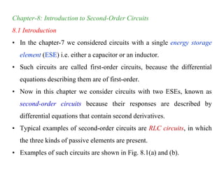
  • 1. Chapter-8: Introduction to Second-Order Circuits 8.1 Introduction • In the chapter-7 we considered circuits with a single energy storage element (ESE) i.e. either a capacitor or an inductor. • Such circuits are called first-order circuits, because the differential equations describing them are of first-order. • Now in this chapter we consider circuits with two ESEs, known as second-order circuits because their responses are described by differential equations that contain second derivatives. • Typical examples of second-order circuits are RLC circuits, in which the three kinds of passive elements are present. • Examples of such circuits are shown in Fig. 8.1(a) and (b).
  • 2. • Other examples are RL & RC circuits, shown in Fig. 8.1(c) and (d). • It is apparent from Fig. 8.1 that a second- order circuit may have two storage elements of different type or the same type. • Usually two storage elements appear in circuit when elements of the same type cannot be represented by an equivalent single element. • Op amp circuit with two storage elements is also a 2nd-order circuit. • As with first-order circuits, a second-order circuit may contain several resistors and dependent and independent sources.
  • 3. • A second-order circuit is characterized by a second-order differential equation and consists of resistors plus equivalent of two ESEs. • Analysis of second-order circuits is similar to first-order circuits. • We will first consider circuits that are excited by the initial conditions of the storage elements. • Although such circuits may contain dependent sources, they are free of independent sources. • These source-free circuits will give natural responses as expected. • Later we will consider circuits excited by independent sources. • Such circuits yield both the transient and the steady-state response. • We consider only DC independent sources in this chapter. • Case of sinusoidal & exponential sources is deferred to later chapters.
  • 4. • We begin by learning how to obtain the initial conditions for the circuit variables and their derivatives. • Then we consider series and parallel RLC circuits for the two cases of excitation: i.e. by initial conditions of the ESEs and by step inputs. • Later we will examine some other types of second-order circuits. Finding Initial and Final Values • Major problem encountered in handling second-order circuits is finding the initial and final conditions on circuit variables. • Getting the initial and final values of v and i is comparatively easy, but NOT finding the initial values of their derivatives: dv/dt and di/dt. • Hence let us devote some time to understanding the processes of determining v(0), i(0), dv(0)/dt, di(0)/dt, i(), and v().
  • 5. • Unless otherwise stated, v; always denotes capacitor voltage, while the symbol i; always represents the inductor current. • Two key points to keep in mind for defining the initial conditions are, • Firstly; as always in any circuit analysis technique, carefully handle the (1) polarity of voltage v(t) across the capacitor and the (2) direction of the current i(t) through the inductor. • Keep in mind that v and i are defined strictly according to the passive sign convention that was introduced in BEE course. What is PSC? • Secondly; keep in mind that the capacitor voltage as well as and the inductor current is always continuous so that, • v(0+) = v(0-) (8.la). • i(0+) = i(0-) (8.1b).
  • 6. • Where t = 0– denotes time just before a switching event and t = 0+ is the time just after the switching event, assuming that the switching event takes place at t = 0. • Thus, in finding initial conditions, always focus first on those vari- ables that cannot change abruptly, i.e. capacitor voltage & inductor current, i.e. by applying Eq. (8.1). Examples below illustrate the ideas. • Example 8.1; switch in Fig. 8.2 has been closed for a long time. • Switch opens at t = 0. • Find: a) i(0+) and v(0+), b) di(0+)/dt and dv(0+)/dt, c) i() and v().
  • 7. • (a). If the switch is closed a long time before t = 0, it means that the circuit has reached dc steady state at t < 0. • In steady state, inductor is like a short circuit and capacitor an open circuit, so equivalent circuit at t = 0 – would appear as in Fig. 8.3(a). • Applying Ohm’s law, i(0 –) = 12/(4 + 2) = 2 A & v(0 –) = 2i(0 –) = 4 V. • As the inductor current and the capacitor voltage cannot change abruptly, hence, i(0 +) = i(0 –) = 2 A, and v(0 +) = v(0 –) = 4 V. • (b). At t = 0+, switch is open; equivalent circuit is as in Fig. 8.3(b).
  • 8. • Since the same current flows (series connection) through both the inductor and capacitor, hence, iC(0+) = i(0+) = 2 A. • Since C(dv/dt) = iC, it can be expressed as, dv/dt = iC/C. • Hence, at t = 0+, dv(0+)/dt = iC(0+)/C = 2/0.1 = 20 V/s. • Similarly, since L(di/dt) = vL, so it can be expressed as, di/dt = vL/L. • We now obtain vL by applying KVL to the loop in Fig. 8.3(b). • Result is; –12 + 4i(0+) + vL(0+) + v(0+) = 0 or vL(0+) = 12 – 8 – 4 = 0. • Thus, at t = 0+, di(0+)/dt =vL(0+)/L = 0/0.25 = 0 A/s. • (c). For t > 0, the circuit undergoes transient, but as t  , the circuit again reaches in its steady state. • Now inductor acts like a short circuit and the capacitor like an open circuit, thus circuit of Fig. 8.3(b) becomes equivalent to Fig. 8.3(c).
  • 9. • In circuit of Fig 8.3(c), it is obvious that i() = 0 A & v() = 12 V. • Problem 8.1; In Fig. 8.62, find: a. i(0+) and v(0+), b. di(0+)/dt and dv(0+)/dt, c. i() and v(). • At t = 0 – , circuit has reached steady state and the equivalent circuit is as shown in Fig. (a). • Thus, i(0 –) = 12/6 = 2A, and v(0 –) = 12V. • Since inductor current and capacitor voltage can not change suddenly, therefore, • i(0+) = i(0-) = 2A, and v(0+) = v(0-) = 12V a. • For t = 0+, equivalent circuit appear in Fig. (b).
  • 10. • vL = L(di/dt), or once rearranged di/dt = vL/L. • Applying KVL to equivalent circuit, yield, vL(0+) – v(0+) + 10i(0+) = 0 • Substituting i(0+) & v(0+) values provide, vL(0+) – 12 + 20 = 0, • Solving it yield, vL(0+) = – 8 V. • Hence, di/dt = vL/L = – 8/2 = – 4 A/s = di(0+)/dt b. • Similarly when, iC = C(dv/dt), then, dv/dt = iC/C. • Obviously, iC(0+) = – i(0+) and as i(0+) = 2 A, so iC(0+) = – 2 A. • Thus dv/dt = iC/C = – 2/0.4 = – 5 V/s = dv(0+)/dt. c. As t  , circuit reaches steady state, thus i() = 0 A, v() = 0 V. • Home Work: P_Problem 8.1, Problems 8.3, 8.4 and 8.5. • Example 8.2; In circuit of Fig.8.5 find,
  • 11. a. iL(0+), vC(0+), vR(0+), b. diL(0+)/dt, dvC(0+)/dt, dvR(0+)/dt, c. vC(), vR(). • (a). For t < 0, 3u(t) = 0, and obviously the circuit is in steady state. • Hence the inductor can be replaced by a short circuit, while the capacitor is replaced by an open circuit as, shown in Fig. 8.6(a). • From Fig 8.6(a), iL(0-) = 0, vR(0-) = 0, and vC(0-) = –20 V (8.2.1). • Class work; Although the derivatives of above quantities at t = 0- are not asked in the example, can you assess what they would be? • Answer; It is evident that they are all zero, since the circuit has reached steady state and nothing changes.
  • 12. • For t > 0, 3u(t) = 3, so that the circuit is now equivalent to Fig. 8.6(b). • Since inductor current and capacitor voltage cannot change abruptly,  iL(0+) = iL(0-) = 0 and vC(0+) = vC (0-) = –20 V Answer a-1&2 (8.2.2). • Although the voltage across the 4  resistor is not required, we will use it to apply KVL and KCL. • Let it be called vO. • Applying KCL at node a in Fig. 8.6(b) yield nodal equation, • 3 = vR(0+)/2 + vO(0+)/4 (8.2.3). • Applying KVL to middle mesh of Fig. 8.6(b) reveal mesh equation, • –vR(0+) + vO(0+) + vC(0+) + 20 = 0 (8.2.4).
  • 13. • From Eq. (8.2.2), vC (0+) = –20 V, substituting it in Eq. (8.2.4) implies • vR(0+) = vO (0+) (8.2.5). • Relating equivalence established in Eq. (8.2.5) to Eq. (8.2.3) yields,  vR(0+) = vO (0+) = 4 V Answer a-3 (8.2.6). • (b). At t > 0, from L diL/dt = vL, we obtain, diL(0+)/dt = vL(0+)/L. • Applying KVL to the right mesh in Fig. 8.6(b) yield mesh equation, • vL(0+) = vC(0+) + 20 = 0 • Since vC (0+) = –20 V, from Eq. (8.2.2), therefore, vL(0+) = 0.  Hence, diL(0+)/dt = vL(0+)/L = 0/0.6 = 0 Answer b-1 (8.2.7). • Similarly, for C dvC/dt = iC, can be rewritten as dvC/dt = iC/C. • Let us apply KCL at node b in circuit of Fig. 8.6(b) to compute iC.
  • 14. • vO(0+) / 4 = iC(0+) + iL(0+) (8.2.8). • As vO(0+) = 4 (Eq 8.2.6) & iL(0+) = 0, (Eq 8.2.2) so iC(0+) = 4/4 = 1 A.  Hence, dvC(0+)/dt = diC(0+)/C = 1/0.5 = 2 V/s. Answer b-2 (8.2.9). • To get dvR(0+)/dt, apply KCL to node a i.e. 3 = vR/2 + vO/4, • Taking the derivative of each term and setting t = 0+ yields, • 0 = {dvR(0+)/dt}/2 + {dvO(0+)/dt}/4 and multiplying both sides by 4, • 0 = 2 {dvR(0+)/dt} + {dvO(0+)/dt} (8.2.10). • Applying KVL to middle mesh of Fig. 8.6(b) reveal mesh equation. • –vR + vC + 20 + vO = 0 • Again, taking the derivative of each term and setting t = 0+ yields. • – {dvR(0+)/dt} + {dvC(0+)/dt}+ {dvO(0+)/dt} = 0. • Substituting, {dvC(0+)/dt} = 2 V/s, (Eq. 8.2.9), modifies above into,
  • 15. • {dvR(0+)/dt} – 2 = {dvO(0+)/dt} (8.2.11). • Replacing value of {dvO(0+)/dt} from Eq. (8.2.11) into (8.2.10), yield, • [2 {dvR(0+)/dt} + {dvR(0+)/dt} – 2] = 0, which once simplified, yield,  3{dvR(0+)/dt} – 2] = 0,  {dvR(0+)/dt} = 2/3 V/s. Answer b-3 . • Although not asked, we can find diR(0+)/dt as well. (VR  5iR in book) • As iR = vR/2, so, {diR(0+)/dt} = {(1/2)(dvR(0+)/dt} = {(1/2)(2/3) = 2/6 A/s. • (c). As t  , circuit is in steady state, using Fig. 8.6(a) with 3 A source added, • By CDR, iL() = [2/(2 + 4)] x 3 = l A. Answer c-1 .  By CDR & Ohms law, vR() = [4/(2 + 4) x 3] x 2 = 4 V. Answer c-2 .  Due to steady state condition, vC() = – 20 V. Answer c-3 . • Home Work: P_Problem 8.2 and Problem 8.6.
  • 16. Source Free Series RLC Circuit • Understanding the natural response of series RLC circuit provides needed background for studies in filter design and comm-networks. • Consider the series RLC circuit shown in Fig. 8.8. • The circuit has no independent source and is hence excited only by the energy initially stored in the capacitor and inductor. • This energy is represented by the initial capacitor voltage VO and initial inductor current IO. • Thus, at t = 0, • (8.2a). • (8.2b). • Applying KVL to circuit of Fig. 8.8,
  • 17. • (8.3). • Differentiating Eq. (8.3) with respect to t and rearranging terms yield, • (8.4). • Eq. 8.4, is a second-order differential equation and is the reason for calling the RLC circuits as second-order circuits. • To solve a second-order differential equation, similar to Eq (8.4), requires establishing of two initial conditions. • Let the two initial conditions be initial value of i & its first derivative. • The initial value of i as given in Eq. (8.2b) is i(0) = IO. • To determine the first derivative of initial value i, requires manipulation the Eqs. (8.2a) and (8.3). • Let’s start by putting initial value of i in Eq (8.3).
  • 18. • Thus, , which once rearranged can be written, • (8.5). • With the two initial conditions established in Eqs. (8.2b) i.e. i(0) = IO, and (8.5) above, let’s proceed to solve 2nd order differential Eq. (8.4). • Based on our experience with first-order circuits, it would be in order to suggest that the solution of Eq. (8.4) is of exponential form. • So we let, i = Aest (8.6). • Where A and s are constants that need to be determined. • Substituting Eq. (8.6) into Eq. (8.4) and carrying out the necessary differentiations, we obtain, or, • (8.7).
  • 19. • Since i = Aest is the assumed solution we are trying to find, only the expression in parentheses can be zero, hence, we can say that, • (8.8). • This quadratic equation is known as the characteristic equation of the differential Eq. (8.4), as the roots of the equation dictate character of i. • The two roots of Eq. (8.8) are, • (8.9a). • (8.9b). • Refer to appendix C.1 for the formulae to find roots of a quadratic equation. • Because of their association with the natural response of circuit, roots sl & s2 are called natural frequencies, measured in nepers per second.
  • 20. • A more compact way of expressing the roots is as shown below. • (8.10). • Where, (8.11). • o in Eq. 8.11, is known as the resonant frequency or strictly, as the un-damped natural frequency, expressed in radians per second (rad/s). •  is the neper frequency or the damping factor, expressed in nepers per second. In terms of  and o, Eq. (8.8) can be re-written as, • (8.8a). • Variables s & o are quantities that will be discussed frequently. • Two values of s in Eq. (8.10) indicate that there are two possible solutions for i, each of which is of the form of the assumed solution in Eq. (8.6); that is, (8.12).
  • 21. • Eq. (8.4) that we aim to solve is a linear equation, any linear combination of two distinct solutions of i1 & i2 also provide a solution to Eq. (8.4). • A complete or total solution of Eq. (8.4) would therefore require a linear combination of i1 and i2. • Thus, the natural response of the series RLC circuit is given by, • (8.13). • Where the constants Al and A2 are determined from the initial values i(0) and di(0)/dt as given in Eqs. (8.2b) and (8.5). • From Eq. (8.10), we can infer three types of solutions, namely, • If  > o, we have the overdamped case. • If  = o, we have the critically damped case. • If  < o, we have the underdamped case.
  • 22. • In other words, the response is overdamped when the roots of the circuit's characteristic equation are unequal and real, critically damped when the roots are equal and real, and underdamped when the roots are complex. Let’s consider each of these cases separately. Overdamped Case ( > o); • From Eqs. (8.9) and (8.10),  > o implies that C > 4L/R2. • When this happens, both roots s1 and s2 are negative and real. • The response is (8.14). • Which decays and approaches zero as t increases. • Figure 8.9(a) (next slide), illustrates a typical overdamped response. Critically Damped Case ( = o); • when,  = o then C = 4L/R2 and, (8.15).
  • 23. • For this case, Eq. (8.13) yields, • • where A3 = Al + A2. • This can not be the solution, because the two initial conditions cannot be satisfied with the single constant A3. • What then could be wrong? • Our assumption of an exponential solution is incorrect for the special case of critical damping. • Going back to Eq. (8.4), when  =o = R/2L, Eq. (8.4) become,
  • 24. • Or, once rearranged, (8.16). • If we let f = di/dt + i, (8.17). • Then Eq. (8.16) becomes, df/dt + f = 0, which is a 1st-order differential equation with solution f = Ale-t, where Al is a constant. • The Eq. (8.17) then becomes, di/dt + i = Ale-t, which once multiplied by et leaves behind, etdi/dt + e ti = Al (8.18). • Rearranging by product rule lead to (d/dt)(et i) = Al (8.19). • Integrating both sides of Eq. 8.19 yields, (et i) = Alt + A2. • Where A2 is another constant. • Alternatively, it can be rewritten as i = (Alt + A2)e–t (8.20). • Hence, the natural response of the critically damped circuit is a sum of two terms: (1) a negative exponential and (2) a negative exponential multiplied by a linear term, or, i(t) = (A2 + Alt)e-t (8.21).
  • 25. • A typical critically damped response is shown in Fig. 8.9(b). (slide-23) • Fig. 8.9(b) is in fact a sketch of i(t) = te-t, which reaches a maximum value of e-1/ at t = 1/, one time constant & then decays to zero. Underdamped Case ( < o); • For  < o, C < 4L/R2. The roots may be written as, • (8.22a). • (8.22b). • Where and called damping frequency. • Both o and d are natural frequencies as they help determine natural response; while o is often called the un-damped natural frequency, and d is called the damped natural frequency. • The natural response is, , i(t) = A1e-( - j d )t + A2e-( + j d )t (8.23a).
  • 26. • Which can also be written as, i(t) = e-t (A1ejdt + A2e-jdt) (8.23b). • Using Euler’s identities, ej = cos  + j sin  & e– j = cos  – j sin  (8.24). • Eq. (8.23) can be written as, • i(t) = e-t [A1(cos dt + j sin dt) + A2(cos dt – j sin dt)], or else, • i(t) = e-t [(A1 + A2)cos dt + j(A1 – A2)sin dt)] (8.25). • Replacing constants, (A1 + A2) and j(A1 – A2) with constants B1 and B2, respectively, the equation 8.25 can be written as, • i(t) = e-t (B1 cos dt + B2 sin dt) (8.26). • Presence of sine and cosine functions, renders it clear that the natural response for this case is exponentially damped & oscillatory in nature. • The response has a time constant of 1/ and a period of  = 2/d.
  • 27. • Figure 8.9(c) on slide-23, depicts a typical underdamped response. • [Figure 8.9 assumes for each case that i(0) = 0.] • Once the inductor current i(t) is known for the RLC series circuit as shown above, other circuit quantities can easily be found. • For example, the resistor voltage is vR = Ri, and the inductor voltage is vL = L di/dt. Properties of RLC Series Network;  Behavior of RLC network is captured by the idea of damping, which is the gradual loss of the initial stored energy, as evident by the continuous decrease in the amplitude of the response.  The damping effect is due to the presence of resistance R.  Damping factor  determines rate at which the response is damped.
  • 28.  If R = 0, then  = 0, (note that  = R/2L) and we have an LC circuit with 1LC as the undamped natural frequency i.e. O = 1LC, also called resonant frequency.  Such circuit is said to be loss-less, because the dissipating or damping element (R) is absent.  By adjusting the value of R, the response may be made undamped, overdamped, critically damped, or underdamped.  When  < o, the response is not only undamped but also oscillatory.  Oscillatory response is possible due to the presence of the two types of storage elements. Having both L and C allows the flow of energy back and forth between the two.  The damped oscillation exhibited by the underdamped response is known as ringing.
  • 29.  It stems from the ability of the storage elements L and C to transfer energy back and forth between them.  Observe from Fig. 8.9 that the waveforms of the responses differ.  In general, it is difficult to tell from the waveforms the difference between the overdamped and critically damped responses.  The critically damped case is the borderline between the underdamped and overdamped cases and it decays the fastest.  With the same initial conditions, the overdamped case has the longest settling time, because it takes the longest time to dissipate the initial stored energy.  For a response that approaches the final value most rapidly without oscillation or ringing, the critically damped circuit is the right choice.
  • 30. • Example 8.3; In Fig. 8.8, R = 40 , L = 4 H, and C = 1/4 F. Calculate the characteristic roots of the circuit? Is the natural response overdamped, under-damped, or critically damped? • As, • Since  > o, hence response is overdamped. • So, • Thus, s1 = – 0.101, s2 = – 9.899. • This is also evident from the fact that the roots are real and negative. • Home Work; P_Problem 8.3 & Problem 8.7. • Example 8.4; Find i(t) in circuit of Fig. 8.10. Assume that the circuit has reached steady state at t = 0–.
  • 31. • For t < 0, the switch is closed, steady state has reached,the capacitor is open circuit while the inductor acts like a closed circuit. • The equivalent circuit would appear as shown in Fig. 8.11(a). • So, i(0–) = 10/(6 + 4) = 1 A and v(0–) = 6i(0) = 6 V. (VDR also works) • At t = 0, i(0–) = i(0) = 1 A and v(0–) = v(0) = 6 V. • Where i(0) is the initial current through the inductor and v(0) is the initial voltage across the capacitor.
  • 32. • For t > 0, the switch is opened and the voltage source is disconnected. • Resulting source free RLC circuit is shown in Fig. 8.11(b) where equivalent 9  resistor represent added up 3  & 6  series resistors. • To compute the roots, lets first determine the value of  and O, • Using Eq (8.11),  = R/(2L) = 9/(2 x 0.5) = 9, and • O = 1/(LC) = 1/(0.5 x 0.02) = 10. • Since  < , (9 < 10), hence, the response is underdamped. • Now to find the roots we employ Eq. 8.22, i.e. • , putting values yield, • • Once solved, s1,2 = – 9 ± j4.359 = –  + jd.
  • 33. • Applying obtained results in Eq. 8.26, (1st swap constants B to A) i.e. i(t) = e-t (A1 cos dt + A2 sin dt) the natural response is, • i(t) = e-9t(A1 cos 4.359t + A2 sin 4.359t) (8.4.1). • We now obtain Al and A2 using the initial conditions of i(0) and v(0). • At t = 0, Eq, 8.4.1 yield, i(0) = Al =1 (8.4.2). • Employ Eq. (8.5), i.e. , to find the di/dt at t = 0. • (8.4.3). • Note that v(0) = Vo = – 6 V is used, as the polarity of v in Fig. 8.11(b) is opposite that in Fig. 8.8, we employed to derive response. • Taking derivative of i(t) in Eq. (8.4.1), • di/dt = -9e-9t(A1 cos 4.359t + A2 sin 4.359t) + e-9t(4.359)(-A1 sin 4.359t + A2 cos 4.359t)
  • 34. • Imposing the condition established in Eq. (8.4.3) at t = 0 gives, • – 6 = – 9 (A1 + 0) + 4.359 (– 0 + A2). • But Al = 1, Eq. (8.4.2), substituting this value can help find A2 value. • Therefore, – 6 = – 9 + 4.359A2  A2 = 0.6882. • Replacing values of Al and A2 in Eq. (8.4.1) yields the complete solution as, i(t) = e-9t(cos 4.359t + 0.6882 sin 4.359t) A • Home Work: P_Problem 8.4, Problem 8.15 and 8.16. Source-Free Parallel RLC Circuit • Consider the parallel RLC circuit shown in Fig. 8.13. • Then initial inductor current I0 and initial capacitor voltage V0, will be,
  • 35. • (8.27a). • (8.27b). • Being in parallel, all elements have the same voltage v across them. • Applying KCL at the top node yields, • (8.28). • Taking the derivative with respect to t and dividing by C results in, • (8.29). • Following the reasoning, used in establishing Eqs. (8.4) through (8.8), can help develop the characteristic equation for RLC parallel circuit. • Replacing the first derivative by s and the second derivative by s2, yields characteristics (or quadratic) equation, shown as Eq. (8.30).
  • 36. • (8.30). • The roots of above quadratic equations are, • (8.30). • Which can be substituted with, • (8.31). • Where and (8.32). • Names of these terms remain the same as in the preceding section, as they play the same role in the solution. What are these term known as? • Just like the series RLC circuits, in RLC parallel circuit also there are three possible solutions.
  • 37. • The RLC parallel circuit may be over, under or critically damped, depending on the relationship between  and O. • We next consider each case individually. Overdamped Case ( > o) • From Eq. (8.32), for  > o, L > 4R2C. • The roots of the characteristic equation are real and negative. • The response is, (8.33). Critically Damped Case ( = o) • From Eq. (8.32), for  = o, L = 4R2C. • The roots of the characteristic equation are real and equal. • The response is, (8.34). Underdamped Case ( < o) • From Eq. (8.32), for  < o, L < 4R2C.
  • 38. • In this case the roots are complex and may be expressed as, • (8.35). • Where, (8.36). • The response is (8.37). • Al and A2 in each case can be determined, from the initial conditions. • To solve must know, v(0) & dv(0)/dt, v(0) is taken from Eq. (8.27b). • Combining Eqs. (8.27a & b) with (8.28), help compute dv(0)/dt, i.e. • or (8.38). • Voltage waveforms resemble shown in Fig. 8.9 depending on whether the circuit is overdamped, underdamped, or critically damped. • Having found capacitor voltage v(t) as circuit response for the parallel RLC circuit (Eq.8.37), other circuit quantities can be computed easily.
  • 39. • Recall, inductor current i(t) is found first for the RLC series circuit, but we compute capacitor voltage v(t) first for the parallel RLC circuit. • Capacitor Voltage v(t) is selected as the key variable to be determined first in order to take advantage of Eq. (8.1a). • Example 8.5; In the parallel circuit of Fig. 8.13, find v(t) for t > 0, assuming v(0) = 5 V, i(0) = 0, L = 1 H, and C = 10 mF. Consider these cases: R = 1.923 , R = 5 , and R = 6.25 . • CASE 1; when R = 1.923 , then, • As  > o, response is overdamped.
  • 40. • The roots of the characteristic equation are, therefore, • , and, the corresponding response is, • (8.5.1). • Apply initial conditions, t = 0 & v(0) = 5 V to Eq. (8.5.1) and we get, • v(0) = 5 = A1 + A2 (8.5.2). • Employing Eq. (8.38), • Differentiating Eq. (8.5.1), yield, , which, • At t = 0, it will become, (8.5.3). • Solving Eq. (8.5.3) and (8.5.2), yield, Al = – 0.2083 & A2 = 5.208. • Substituting Al and A2 values in Eq. (8.5.1) yield, • (8.5.4).
  • 41. • CASE 2; when R = 5 , then, applying Eq. (8.10 • , and, • • As  = o , response is critically damped, roots are, s1 = s2 = – 10, and, • (8.5.5). • Applying initial conditions, t = 0 & v(0) = 5 V to Eq. (8.5.5), yield, • (8.5.6). • By Eq. (8.38), • Differentiating Eq. (8.5.5), yield, • Which at t = 0, becomes, (8.5.7). • From Eqs. (8.5.6) and (8.5.7), Al = 5 and A2 = – 50.
  • 42. • Thus, v(t) = (5 – 50t)e-10t V (8.5.8). • CASE 3: When R = 6.25 , , and, . • As  < o in this case, the response is underdamped. • Roots of characteristic equation, are, • Hence, (8.5.9). • At t = 0 & v(0) = 5 V, Eq. (8.5.9) yield, v(0) = 5 = Al (8.5.10). • By Eq. (8.38), • Differentiating Eq. (8.5.9), yield, • • Which at becomes, t = 0, – 80 = – 8A1 + 6A2 (8.5.11).
  • 43. • Solving Eqs. (8.5.10) and (8.5.11), we find, Al = 5 and A2 = – 6.667. • Thus, v(t) = (5 cos 6t - 6.667 sin 6t)e-8t (8.5.12). • Notice that by increasing value of R, the degree of damping decreases & responses differ. • Figure 8.14 plots the three cases.
  • 44. • Home Work: P_Problem 8.5. • Example 8.6; Find v(t) for t > 0 in the RLC circuit of Fig. 8.15. • When t < 0, the switch is open; • Now inductor acts like a short and capacitor as open circuit. • The initial voltage across the capacitor is the same as the voltage across the 50  resistor; that is, • (8.6.1). • The initial current through the inductor is, • Direction of inductor current i as indicated in Fig. 8.15 is in line with the direction of inductor current I0 in Fig. 8.13, which conforms to convention that current flows into the positive terminal of an inductor.
  • 45. • Employing eq. (8.38), we can next determine the dv/dt, • By Eq. (8.38), (8.6.2). • At t > 0, the switch is closed and the voltage source along with 30  resistor is separated from the rest of the circuit. • The parallel RLC circuit acts independently of the voltage source, as illustrated in Fig. 8.16, i.e. it is a source free circuit. • • • As  > , hence the response of the circuit is overdamped.
  • 46. • We next compute the roots of the appropriate characteristics equation. • , substituting the values yield, • • Solving it reveal, • Since the circuit has overdamped response, hence, • (8.6.3). • At t = 0, impose the condition listed in Eq. (8.6.1), i.e. v(0) = 25 V. • v(0) = 25 = Al + A2 Or A2 = 25 – Al (8.6.4). • Taking the derivative of v(t) in Eq. (8.6.3), provides, • • Imposing the condition in Eq. (8.6.2),
  • 47. • Or, 0 = 854A1 + 146A2 (8.6.5). • Solving Eqs. (8.6.4) and (8.6.5) gives, Al = – 5.156 and A2 = 30.16. • Substituting these values in Eq. (8.6.3) provide complete solution as, • • Home Work: Problems 8.23 and 8.31. Step Response of a Series RLC Circuit • Recall, step response is obtained by sudden application of a dc source. • Consider the series RLC circuit shown in Fig. 8.18. • Applying KVL around the loop for t > 0, yield, • (8.39)
  • 48. • However, series current flowing in the circuit is, • Replace this value of i in Eq. (8.39) & divide both sides by LC to get, • (8.40). • It has same coefficients as Eq. (8.4), i.e. the 2nd order differential equation drawn for series RLC circuit, only the variables are different. • Coefficient similarity is key to determining the frequency parameters. • Hence, it can be concluded that the characteristic equation for the series RLC circuit is NOT affected by the presence of the dc source. • The solution to Eq. (8.40) has two components: (1) the transient response vt(t) and (2) the steady-state response vss(t); that is to say, • (8.41). • Transient response vt(t) is part of total response that dies out with time
  • 49. • The form of the transient response is the same as the form of the solution obtained (in Section 8.3) for the source-free circuit, evident by Eqs. (8.14), (8.21), and (8.26). • Therefore, the transient response vt(t) for the overdamped, underdamped, and critically damped cases are: • (8.42a). • (8.42b). • (8.42c). • The steady-state response is the final value of v(t). • In the circuit in Fig. 8.18, the final value of the capacitor voltage is the same as the source voltage Vs. Hence, • (8.43).
  • 50. • Thus, the complete solution for the overdamped, underdamped, and critically damped cases are: • (8.44a). • (8.44a). • (8.44a). • The values of the constants Al and A2 are obtained from the initial conditions i.e. v(0) and dv(0)/dt. • Keep in mind that v and i are, respectively, the voltage across the capacitor and the current through the inductor. • Therefore, Eq. (8.44) only applies for finding v. • Once capacitor voltage vC = v is known, current i can be determined.
  • 51. • Series circuit current is given by i = C dv/dt, which is the same current through the capacitor, inductor, and resistor. • Hence, the voltage across the resistor is vR = iR, while the inductor voltage is vL = L di/dt. • Alternatively, the complete response for any variable x(t) can be found directly, as it has the general form, x(t) = xss(t) + xt(t) (8.45). • Where, xss = x() is the final value and xt(t) is the transient response. • Final value is found as in Section 8.2 (Finding Initial & Final Values). • Transient response has the same form as in Eq. (8.42), and the associated constants are determined from Eq. (8.44) based on the values of x(0) and dx(0)/dt. • Example 8.7: For the circuit in Fig. 8.19, find v(t) and i(t) for t > 0.
  • 52. • Consider three cases: R = 5 , R = 4 , and R = 1 . • CASE 1: When R = 5 . • For t < 0, switch is closed for long time. • Circuit is in steady state, the capacitor behaves like an open circuit while the inductor acts like a short circuit. • The initial current through the inductor i(0) = 24 / (5 + 1) = 4 A. • The initial voltage across the capacitor is the same as the voltage across the 1  resistor; that is, v(0) = 1.i(0) = 4 V. • For t > 0, the switch is opened, the 1 resistor gets disconnected leaving behind a series RLC circuit with the voltage source. • The characteristic roots can now be determined as follows:
  • 53. • and • Therefore, the roots are, • Since  > O, the circuit has overdamped natural response. • The total response is therefore, given by, • Where vSS, is final value of capacitor voltage, i.e. vf = 24 V. • Thus, (8.7.1). • Applying initial conditions at t = 0, yield • Which once rearranged provide, – 20 = Al + A2 (8.7.2). • Current through inductor can’t change abruptly and being in series the capacitor current can’t change as well. Hence at t = 0+, •
  • 54. • Derivative of v in Eq. (8.7.1) i.e. , yield, • (8.7.3). • At t = 0, (8.7.4). • Solving Eqs. (8.7.2) and (8.7.4), yield, Al = – 64/3 and A2 = 4/3. • Substituting Al and A2 values in Eq. (8.7.1), we get at t > 0, • (8.7.5). • Since the inductor and capacitor remain in series for t > 0, the inductor current is the same as the capacitor current. Hence, . • Multiplying Eq. (8.7.3) by C = 0.25 and substituting Al and A2 values gives back; (8.7.6). • Note that i(0) = 4 A as expected.
  • 55. • CASE 2: When R = 4, now the initial current through the inductor is . • And the initial capacitor voltage is v(0) = 1.i(0) = 4.8 V. • Also, , while O = 2 remains same. • Characteristic roots are, s1 = s2 = - = -2, and we have critically damped natural response. Why? (As  = , also –ve and real root). • The total response is therefore, given by . • As before, final capacitor voltage vf = and response is, • (8.7.7). • To find Al and A2, we use the initial conditions. • We write, (8.7.8). • Since i(0) = C dv(0)/dt = 4.8, hence,
  • 56. • From Eq. (8.7.7), (8.7.9). • At t = 0, (8.7.10). • From Eq. (8.7.8) putting Al = –19.2 in Eq. (8.7.10), yield A2 = – 19.2. • Thus, Eq. (8.7.7) becomes, (8.7.11). • Inductor current is same as the capacitor current; i.e. . • Multiplying Eq. (8.7.9) by C = 0.25 and substituting the values of Al and A2 gives back, (8.7.12). • Note that i(0) = 4.8 A, as expected. • CASE 3: When R = 1 . • At t < 0, the initial inductor current is, . • The initial voltage across the capacitor is the same as the voltage across the 1 resistor, i.e. v(0) = 1.i(0) = 12 V.
  • 57. • Now, , while O = 2 remains unchanged. • Since  < O, circuit has the underdamped response. • Characteristic roots are, • Total response is therefore, given by . • As before, final capacitor voltage vf = • Substituting the known values, total response can be expressed as,, • (8.7.13). • At t = 0 and employing initial value of voltage v(0) = 12, Eq. 8.7.13 can be rewritten as, • Solving it reveal A1 = –12 (8.7.14).
  • 58. • Initial value of current i(0) = C dv(0)/dt = 12, reveal the derivative of v(0) as, (8.7.15). • Putting known values of  = 0.5 and d = 1.936 in total response equation, transforms it into, • …………… (8.7.16). • At t = 0, it would change to, • Swap Al = – 12, find A2 = 21.694, replace them in Eq. (8.7.13) & get, • . (8.7.17).
  • 59. • As iC = i(t) = C(dv/dt), C = 0.25, Al = – 12 & A2 = 21.694 are known. • So product of Eq. (8.7.16) & C with substituted A1 & A2 values yield, • and dv/dt is given by Eq. (8.7.16). (8.7.18). • As expected i(0) = 12 A. • Figure 8.20 plots the responses for three cases. • From this figure you can observe that the critically damped response reaches the step input of 24 V the fastest. • Home Work: P_Problem 8.7.
  • 60. Step Response of a Parallel RLC Circuit • Aim is to find current i resulting from sudden application of a dc current in the parallel RLC circuit shown in Fig. 8.22. • For t > 0, switch is open. Applying KCL at the top node reveal. • (8.4.6). • Substituting in Eq. (8.46) and dividing it by LC, reveals, • (8.4.7). • Which has the same characteristic equation as Eq. (8.29). • The complete solution to Eq. (8.47) again consists of the transient response it(t) and the steady-state response iss; that is, • (8.4.8).
  • 61. • Transient response is the same as what was observed in Section 8.4. • The steady-state response is the final value of i. • In the circuit in Fig. 8.22, the final value of the current through the inductor is the same as the source current IS. Thus, • (8.4.9). • (8.4.9). • (8.4.9). • The constants Al and A2 in each case can be determined from the initial conditions for i and its derivaqtive di/dt. • Note that Eq. (8.49) again, applies only for finding inductor current i. • But once the inductor current iL = i is known, we can find v = L di/dt, which is the same voltage across inductor, capacitor, and resistor. Why?
  • 62. • Hence, the current through the resistor is iR = v/R, while the capacitor current is iC = C dv/dt. • Alternatively, the complete response for any variable x(t) may be found directly, using, (8.50). • Where xSS, and xt are its final and transient responses, respectively. • Example 8.8; In the circuit of Fig. 8.23, find i(t) and iR(t) for t > 0 ? • For t < 0, the switch is open, and the circuit is partitioned into two independent sub circuits. • As 4 A current flows in the inductor, hence, i(0) = 4 A. • Voltage source 30u(-t) = 30 when t < 0 and 0 when t > 0.
  • 63. • Therefore, the voltage source is operative for t < 0. • Capacitor acts like an open circuit and the voltage across it is the same as the voltage across the 20  resistor connected in parallel with it. • By VDR, initial capacitor voltage is, . • For t > 0, the switch is closed, resulting in a parallel RLC circuit with a current source. • The voltage source is zero which means it acts like a short-circuit. • The two 20  resistors are now in parallel. • They are combined to give R = 20 || 20 = 10 . • The characteristic roots are determined as follows: • •
  • 64. • • • • Thus, • As  > O, we have the overdamped case, so applying Eq. (6.49) give • Current, (8.8.1). • Where IS = 4 A is the final value of i(t). • We now use the initial conditions to determine Al and A2. • At t = 0, i(0) = 4 = 4 + Al + A2  A2 = -A1 (8.8.2). • Taking the derivative of i(t) at t = 0, in Eq. (8.8.1), yield, • (8.8.3). • But,
  • 65. • Substituting this into Eq. (8.8.3) and incorporating Eq. (8.8.2), we get 0.75 = (11.978 - 0.5218)A2  A2 = 0.0655. • Thus, Al = – 0.0655 and A2 = 0.0655. • Inserting Al and A2 in Eq. (8.8.1) gives the complete solution i.e. • • From i(t), we obtain v(t) = L di/dt and, • • Home Work: P_Problem 8.8, Problems 8.45 and 8.49 General Second-Order Circuits • Having learned series and parallel RLC circuits, we are prepared to apply the practiced ideas to any second-order circuit having one or more independent sources with constant values.
  • 66. • Given any second-order circuit, we determine its step response x(t) (which may be voltage or current) by taking the following four steps: 1 We first determine the initial conditions x(0) and dx(0)/dt and the final value x(), as discussed in Section 8.2. 2 We turn off the independent sources and find the form of the transient response xt(t) by applying KCL and KVL. 2 Once a second-order differential equation is obtained, we determine its characteristic roots. 2 Depending on whether the response is overdamped, critically damped, or underdamped, we obtain xt(t) with two unknown constants as we did in the previous sections. 3 We obtain the steady-state response as, (8.51).
  • 67. 3 Where x() is the final value of x, obtained in step 1. 4 The total response is now found as the sum of the transient response and steady-state response (8.52). 4 We finally determine the constants associated with the transient response by imposing the initial conditions x(0) and dx(0)/dt, determined in step 1. • We can apply this general procedure to find the step response of any second-order circuit. The following examples illustrate the four steps. • Example 8.9: Find the complete response v and then i for t > 0 in the circuit of Fig. 8.25. • We first find the initial & final values.
  • 68. • At t < 0, the switch is open. • Circuit is in steady state & equivalent circuit is shown in Fig. 8.26(a). • Clearly, v(0-) = 12 V and i(0-) = 0. • At t = 0+, the switch is closed, the equivalent circuit is as in Fig. 8.26(b). • By the continuity of capacitor voltage and inductor current, we know that • Voltage v(0+) = v(0-) = 12 V and current i(0+) = i(0-) = 0 (8.9.1). • To get dv(0+)/dt, we use C dv/dt = iC, by rearranging it into, dv/dt = iC/C. •
  • 69. • Applying KCL at node a in Fig. 8.26(b) • • Hence, (8.9.2). • The final values are obtained when the inductor is replaced by a short circuit and the capacitor by an open circuit in Fig. 8.26(b), giving, • (8.9.3). • Next, we obtain the form of the transient response for t > 0. • By turning off the 12 V voltage source, we have the circuit as in Fig. 8.27. • Applying KCL at node a in Fig. 8.27 gives, (8.9.4). • Applying KVL to the left mesh, yield,
  • 70. • (8.9.5). • Now to find value of v, substitute i from Eq. (8.9.4) into Eq. (8.9.5) and obtain, • Solving it leaves, • We obtain the characteristic equation as, , with roots s1 = – 2 and s2 = – 3. • Thus, the natural response is (8.9.6). • Where A and B are unknown constants to be determined later. • Steady-state response is (8.9.7). • Complete response is (8.9.8). • To find A and B we use initial values from Eq. (8.9.1) i.e. v(0) = 12.
  • 71. • Substituting v(0) = 12 into Eq. (8.9.8) at t = 0 gives, • (8.9.9). • Taking the derivative of v in Eq. (8.9.8), provides, • (8.9.10). • Substituting Eq. (8.9.2) into Eq. (8.9.10) at t = 0 gives, • (8.9.11). • Eqs. (8.9.9) & (8.9.11), yield, A = 12 & B = -4, so that Eq. (8.9.8) becomes, (8.9.12). • From v, we can compute other quantities of interest by referring to Fig. 8.26(b). To obtain i, for example, • Solving, i for t > 0 (8.9.13).
  • 72. • Note that i(0) = 0, agrees with Eq. (8.9.1). • Home Work: P_Problem 8.9 & Problem 8.53. • Example 8.10: Find vo(t) for t > 0 in the circuit of Fig. 8.29? • This is an example of a second-order circuit with two inductors. • We first obtain the mesh currents i1 and i2, which happen to be the currents through the inductors. • We need to obtain the initial and final values of these currents. • For t < 0, 7u(t) = 0, therefore, • i1(0-) = 0 = i2(0-). • For t > 0, 7u(t) = 7 V, & equivalent circuit is as shown in Fig. 8.30(a).
  • 73. • Due to the continuity of inductor current, • (8.10.1). • (8.10.2). • Applying KVL to the left loop in Fig. 8.30(a) at t = 0+, • or . • Since L1 dil /dt = vL1 , so, (8.10.3). • Also as L2 di2 /dt = vL2 , so, (8.10.4). • As t  , circuit reaches steady state, and inductors can be replaced by short circuits, as shown in Fig. 8.30(b). From this figure, • i1() = i2() = 7/3 A (8.10.5).
  • 74. • Next, obtain the form of the transient responses by removing the voltage source, as shown in Fig. 8.31. • Applying KVL to the two meshes yields, • (8.10.6). • And (8.10.7). • From Eq. (8.10.6), ( 8.10.8). • Substituting Eq. (8.10.8) into Eq. (8.10.7) gives • or, • From this we obtain the characteristic equation as, • Which has roots s = – 3 and s = – 10, hence, the form of the transient response is (8.10.9).
  • 75. • A and B in Eq. (8.10.9) are constants. • The steady-state response is (8.10.10). • From Eqs. (8.10.9) and (8.10.10), we obtain the complete response as, • (8.10.11). • We finally obtain A and B from the initial values. • From Eqs. (8.10.1) and (8.10.11), (8.11.12). • Taking the derivative of Eq. (8.10.11), setting t = 0 in the derivative, and enforcing Eq. (8.10.3), we obtain, (8.11.13). • From Eqs. (8.10.12) and (8.10.13), A = – 4/3 and B = – 1, thus, • (8.11.14). • Next we obtain i2 from i1. Applying KVL to the left loop in Fig. 8.30(a) gives, .
  • 76. • Substituting for i1 in Eq. (8.10.14) gives, • (8.10.15). • From Fig 8.29, (8.10.16). • Substituting Eqs. (8.10.14) and (8.10.15) into Eq. (8.10.16) yields, • (8.10.17). • Note that vo(0) = 0, as expected from Eq. (8.10.2). • Home Work: P_Problem 8.10 and Problem 8.57. • We skip sections 8.8 (op amp as 2nd order circuits) and 8.9 (P_spice analysis of 2nd order circuits) and move on to section 8.10. Duality • The concept of duality is a time-saving, effort-effective measure of solving circuit problems.
  • 77. • Consider the similarity between Eq. (8.4) i.e. and Eq. (8.29) i.e. . • The two equations are the same, except that we must inter-change the following quantities: (1) voltage and current, (2) resistance and conductance, (3) capacitance and inductance. • Thus, it sometimes occurs in circuit analysis that two different circuits have the same equations and solutions, except that the roles of certain complementary elements are interchanged. • This interchangeability is known as the principle of duality. • The duality principle asserts a parallelism between pairs of characterizing equations and theorems of electric circuits. • Dual pairs are shown in Table 8.1 on next slide.
  • 78. • Note that power does not appear in Table 8.1, because power has no dual. • The reason for this is the principle of linearity; since power is not linear, duality does not apply. • Also notice that the principle of duality extends to circuit elements, configurations, and theorems. • Note that even when the principle of linearity applies, a circuit element or variable may not have a dual. • For example, mutual inductance (covered in Chapter 13) has no dual. • Two circuits described by equations of the same form, but in which the variables are interchanged, are said to be dual to each other.
  • 79. • Usefulness of the duality principle is self-evident. • Once we know the solution to one circuit, we automatically have the solution for the dual circuit. • It is obvious that the circuits in Figs. 8.8 and 8.13 (i.e. source free RCL series and parallel circuits) are dual. • Consequently, the result (values of  and O) in Eq. (8.32) is the dual of that in Eq. (8.11). • We must keep in mind that the method described here for finding a dual is limited to planar circuits. • Finding a dual for a non-planar circuit is beyond the scope of this textbook because nonplanar circuits cannot be described by a system of mesh equations.
  • 80. • To find the dual of a given circuit, we do not need to write down the mesh or node equations. • We can use a graphical technique. • Given a planar circuit, we construct the dual circuit by taking the following three steps: • Place a node at the center of each mesh of the given circuit. • Place the reference node (the ground) of the dual circuit outside the given circuit. 1. Draw lines between the nodes such that each line crosses an element. 2. Replace that element by its dual (see Table 8.1). 3. To determine the polarity of voltage sources and direction of current sources, follow the rule,
  • 81. • A voltage source that produces a positive (clockwise) mesh current has as its dual a current source whose reference direction is from the ground to the non-reference node. • In case of doubt, one may verify the dual circuit by writing the nodal or mesh equations. • The mesh (or nodal) equations of the original circuit are similar to the nodal (or mesh) equations of the dual circuit. • The duality principle is illustrated with the following two examples. • Example 8.14: construct the dual of the circuit in Fig. 8.44. • We first locate nodes 1 and 2 in the two meshes.
  • 82. • Also locate ground node 0 for the dual circuit, as in Fig. 8.45(a). • First draw a line between one node and another crossing an element. • Next replace the line joining the nodes by the duals of the elements which it crosses. • For example, a line between nodes 1 and 2 crosses a 2-H inductor, and we place a 2-F capacitor (an inductor's dual) on the line.
  • 83. • A line between nodes 1 and 0 crossing the 6-V voltage source will contain a 6-A current source. • By drawing lines crossing all the elements, we construct the dual circuit on the given circuit as in Fig. 8.45(a). • The dual circuit is redrawn in Fig. 8.45(b) for clarity. • Home Work: P_Problem 8.14 and Problem 8.74. • Example 8.15: Obtain the dual of the circuit in Fig. 8.48? • The dual circuit is constructed on the original circuit as in Fig. 8.49(a).
  • 84. • First locate nodes 1 to 3 and the reference node 0. • Joining nodes 1 and 2, cross the 2-F capacitor, which is replaced by a 2-H inductor. • Joining nodes 2 and 3, cross the 20  resistor, which is replaced by a 1/20  resistor.
  • 85. • keep doing this until all the elements are crossed. • The result is in Fig. 8.49(a). • The dual circuit is redrawn in Fig. 8.49(b). • To verify the polarity of the voltage source and the direction of the current source, apply mesh currents i1, i2, and i3 (all in the clockwise direction) in the original circuit of Fig. 8.48. • The 10 V voltage source produces positive mesh current i1, so that its dual is a 10 A current source directed from 0 to 1. • Also, i3 = – 3 A in Fig. 8.48 has as its dual v3 = – 3 V in Fig. 8.49(b). • Home Work: P_Problem 8.15 and Problem 8.75. • Self Study: Applications of second order circuits (8.11), review questions 8.1 through 8.10.