Similar to [doi 10.1002_9781118886502.ch7] Lehr, Jane; Ron, Pralhad -- Foundations of Pulsed Power Technology __ Energy Storage in Capacitor Banks.pdf (20)
2. 332 Foundations of Pulsed Power Technology
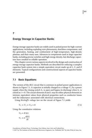
Figure 7.1 A capacitor or bank of capaci
tors with capacitance C is initially charged
to a voltage V0 and discharged through an
inductor and resistance can represent
many pulsed power circuits. The induc
tance and resistance may be the intrinsic
values of the nonideal circuit.
Equation 7.1 is expressed as
di t†
Vc ‡ L ‡ R i t† ˆ 0 (7.2)
dt
Differentiating (7.2) with respect to time yields
dVC d2
i t† di t†
‡ L ‡ R ˆ 0 (7.3)
dt dt2 dt
And the constitutive relation for the capacitor provides a relationship between
the voltage drop and the current
dVC t†
i t† ˆ C (7.4)
dt
Inserting (7.4) into (7.3) and rearranging terms,
d2
i t† R di t† 1
‡ ‡ i t† ˆ 0 (7.5)
dt2 L dt LC
This can be expressed in a convenient form by defining
R
α ˆ (7.6)
2L
and
1
ω0 ˆ p (7.7)
LC
so that (7.5) may be expressed as
d2
i t† di t†
‡ 2α ‡ ω0
2
i t† ˆ 0 (7.8)
dt2 dt
The quantity α is called the attenuation factor and, in traditional circuits, is a
measure of how fast the transient response dies away when the source is
removed. The natural frequency of the circuit is ω0. The solutions for (7.8) are a
superposition of exponentials
s1t
‡ A2es2t
i t† ˆ A1e (7.9)
3. 333
7 Energy Storage in Capacitor Banks
Solving (7.8) in the Laplace domain, the solutions of s1 and s2 are
s1; s2 ˆ α α2 ω2 (7.10)
0
so that the specific forms of the solutions depend on the relative values of α and
ω0 and the constants A1 and A2 are determined by the initial conditions. It is
useful to define the quantity ξ
α
ξ ˆ (7.11)
ω0
which can be related back to the parameters of the RLC circuit through (7.6) and
(7.7),
R C
ξ ˆ (7.12)
2 L
The solutions to (7.9) given in (7.10) can be expressed in terms of ξ as
s1; s2 ˆ α ω0 ξ2
1 ˆ ω0 ξ ξ2
1 (7.13)
The value of the quantity ξ determines the transient behavior of the circuit.
Four cases are relevant:
Ideal (lossless) case ξ ˆ 0
Overdamped response ξ 1
Underdamped response ξ 1
Critically damped case ξ ˆ 1
7.1.1 Case 1: Lossless, Undamped Circuit ξ ˆ 0
In this case, ξ ˆ 0, α ˆ 0, and R ˆ 0. From (7.8), the differential equation
describing the circuit operation becomes
d2
i t†
‡ ω2
0i t† ˆ 0 (7.14)
dt2
The solutions are in the form
i t† ˆ A1 sin ω0t† ‡ A2 cos ω0t† (7.15)
When the switch closes at t ˆ 0, the current is zero. Applying the initial
condition that the current through an inductor cannot change instantane
ously,
iL 0 † ˆ iL 0‡† ˆ 0 (7.16)
A1 sin 0† ‡ A2 cos † ˆ
0 A1 0 † ˆ 0
† ‡ A2 1
4. 334 Foundations of Pulsed Power Technology
and A2 ˆ 0
The other constant A1 is determined by the initial condition on the capacitor:
Vc 0 † ˆ Vc 0‡† (7.17)
Since there is no current flowing in the circuit at t ˆ 0‡,
Vc 0‡† ˆ VL † ˆ
0‡ V0 (7.18)
The negative sign in (7.18) reflects the sign convention adopted in Figure 7.1
that the voltage drop opposes the direction of current. Applying the initial
condition yields
di
VL 0† ˆ L ˆ L A †
‰ 1ω0 cos 0 Š ˆ V0
dt tˆ0
yielding A1 ˆ V0
. The solution for the lossless case is
ω0L
V0
i t† ˆ sin ω0t† (7.19)
ω0L
The time to peak current Tpeak can be calculated by setting the argument of the
sine wave in (7.19) equal to π=2 giving
π p
Tpeak ˆ LC (7.20)
2
Although lossless circuits cannot be fully realized in practice, it is an important
case for circuits requiring high peak currents. Large peak currents may be
produced with a high-capacitance, low-inductance bank where the capacitors
are arranged in parallel, which has the dual benefit of increasing the equivalent
capacitance and reducing the equivalent inductance of each individual capaci
tor. The peak current of such a bank can be estimated from
V0 C
Ipeak ˆ ˆ V0 (7.21)
L
ω0L
This result may also be obtained by considering that for a lossless, undamped
circuit, the stored energy remains constant and alternates between capacitive
energy (1/2CV2
) and inductive energy (1/2LI2
).
7.1.2 Case 2: Overdamped Circuit ξ 1
In this case, from (7.13), the roots of the solution are real and the solution has
the form
i t† ˆ A1 exp ξ ‡ ξ2
1 t ‡ A2 exp ξ ξ2
1 t
ω0 ω0
(7.22)
5. 335
7 Energy Storage in Capacitor Banks
Defining
ξ2
1 (7.23)
ωD ˆ ω0
and recognizing that
ω0ξ ˆ α (7.24)
the solution (7.22) can be expressed as
αt αt ωDt
i t† ˆ A1e eωDt
‡ A2e e
Applying the initial condition (7.16) on the current through the inductor yields
A2 ˆ A1
ωDt
e ωDt
i t† ˆ A1e αt
e (7.25)
Applying the initial condition (7.17) on the voltage across the capacitor to (7.25)
yields
V0
A1 ˆ
2ωDL
And the solution for the underdamped case is
V0 αt ωDt
e ωDt
i t† ˆ e e (7.26)
2ωDL
The overdamped solution may be written as
V0 αt
i t† ˆ sinh ωDt† ? e (7.27)
ωDL
The damping frequency ωD can be expressed in terms of the circuit parame
ters as
ωD ˆ ω0
R2
4
?
L
C
1 ˆ
R2
4L
1
LC
(7.28)
In terms of ω0 and ξ, the current is
i t† ˆ
V0
2ω0L ξ2
1
p
exp ω0 ξ ‡ ξ2
1 t exp ω0 ξ ξ2
1 t
(7.29)
The overdamped case is the discharge without oscillation.
6. 336 Foundations of Pulsed Power Technology
7.1.3 Case 3: Underdamped Circuit ξ 1
p
The solution to the underdamped case occurs when the term ω0 ξ2
1 is
imaginary. Using the defined relationships of (7.22) and (7.33), the solution to
the underdamped circuit response is
αt jωDt
‡ A αt jωDt
i t† ˆ A1e e 2e e (7.30)
p
and j ˆ 1
The solution (7.30) can be written as
αt
A
i t† ˆ e 1 sin ωDt ‡ A2 cos ωDt† (7.31)
Again, applying the initial condition across the inductor,
A2 ˆ 0
Again, applying the initial condition on the capacitive voltage,
V0
A1 ˆ
ωDL
And the solution for the underdamped case is
V0
i t† ˆ e αt
sin ωDt (7.32)
ωDL
The underdamped case is an oscillatory wave with frequency ωD in a decaying
envelope determined by the attenuation constant α. In high-energy circuits, the
underdamped response is usually avoided since a significant voltage reversal
can occur across the capacitors leading to their failure.
7.1.4 Case 4: Critically Damped Circuit ξ ˆ 1
p
In the critically damped case, ξ2
1 ˆ 0, and the roots to (7.13) are
s1; s2 ˆ ω0ξ ˆ α
Taking the inverse Laplace transform, the solution takes the form
αt
i t† ˆ A1t e αt
‡ A2e
Invoking the initial condition on the current through the inductor yields
A2 ˆ 0, and applying the initial condition on the voltage across the inductor
at t ˆ 0,
V0
i t† ˆ t e αt
(7.33)
L
The critically damped response represents the circuit response that decays the
fastest without oscillation. There is generally too much uncertainty in a pulsed
power driver to achieve critical damping.
7. 337
7 Energy Storage in Capacitor Banks
7.1.5 Comparison of Circuit Responses
The current in the RLC circuit representing a capacitor bank is shown in
Figure 7.2. The representative circuit has a capacitance of 10 μF, charged to an
initial voltage of 100 kV with an equivalent inductance of 100 nF. The response
of the circuit depends on the value of the resistance and is encompassed in the
parameter ξ.
The current in the critically damped circuit may be used for a reference and
is represented in Figure 7.2 with ξ ˆ 1. The resistance to critically damp the
circuit can be calculated from (7.12) and for the circuit parameters given, it is
200 mΩ. The underdamped responses, where ξ 1, have larger peak currents
than the critically damped response and oscillatory behavior. Capacitor banks
may be designed to achieve these large peak currents and then use a crowbar
switch to protect the circuit against the large voltage swings from the
oscillations. The overdamped responses are shown in Figure 7.2 with ξ
1 with no oscillations and lower peak currents due to the higher loss in the
circuit. It may be noted that the peak current in the lossless (undamped) case
is 100 kA.
Figure 7.2 The time-dependent current i t† through the circuit of Figure 7.1 when C ˆ 10 μF,
L ˆ 100 nH, and V0 ˆ 100 kV for a range of values for ξ.
8. 338 Foundations of Pulsed Power Technology
7.2 Capacitor Bank Circuit Topology
A typical system layout for a high-energy storage capacitor bank is shown in
Figure 7.3. The energy storage capacitor is charged to a voltage V0 by a power
supply. The discharge sequence is started by a command trigger sent to the start
switch, initiating the discharge of the capacitor bank. The discharge current is
carried by transmission line and delivered to the load through a power feed.
A crowbar switch is often included in the capacitor bank circuit topology as a
protection element. The crowbar switch is arranged so that it closes at a time
after the main discharge has passed and provides a short circuit across the
element to be protected. The crowbar is often used in series with a resistor to
dissipate the excess energy.
The placement of a crowbar switch is determined by its purpose. For
instance, high-energy density capacitors are susceptible to failure from exces
sive voltage reversal. In this case, the crowbar switch is placed as close to the
capacitor as possible, often between the capacitor and the start switch. This
allows only the desired current to go through the start switch, prolonging its life
by minimizing erosion. Other applications, such as plasma confinement or high
magnetic field generation, demand unidirectional current in an underdamped
inductive load so that the crowbar is incorporated across the load. The crowbar
switch may be self-breaking or externally triggered. Some applications, such as
flux compression generators, may design the load to short itself during opera
tion, essentially acting as a crowbar.
Crowbar switches can be difficult to implement in many instances because
they must stay open while the main discharge is occurring and then close upon
the command trigger when the voltage on the crowbar switch may be much
lower. In many applications, the crowbar switch must trigger reliably at low
percentages of its self-breakdown voltage.
Figure 7.3 The circuit topology of an energy storage capacitor bank with a crowbar switch
across the load. A crowbar switch protects the capacitor from excessive voltage reversal.
9. 339
7 Energy Storage in Capacitor Banks
7.2.1 Equivalent Circuit of a Low-Energy Capacitor Bank
A circuit schematic of a low-energy capacitor bank is shown in Figure 7.4. It is
comprised of energy storage capacitor Cs, start-charged through a resistor R to a
voltage V0, and discharged through the start switch Ss. A transmission line TL
delivers the discharge current to the load LLoad, which is protected by a crowbar
switch Scb and energy dissipating resistor Rd.
The various symbols used in the equivalent circuit are as follows:
Capacitor: Lc—equivalent series inductance of Cs
Rc—equivalent series resistance of Cs
Start switch: Lsw—self-inductance of the switch SS
Rsw—internal resistance of the switch SS
Transmission line: LTL—inductance of transmission line of length ℓ
RTL—resistance of transmission line of length ℓ
Crowbar switch: Lcb—self-inductance of crowbar switch
Rcb—internal resistance of crowbar switch
Rd—damping resistance in the crowbar circuit
Load: LLoad—inductance of the load
RLoad—resistance of the load
Prior to triggering the crowbar switch, the operation of the equivalent circuit
in Figure 7.5 can be simplified to apply the equations of Section 7.1 with the
following modifications:
L ˆ Lc ‡ Ls ‡ LTL ‡ LLoad
R ˆ Rc ‡ Rs ‡ RTL ‡ RLoad
The resultant modified equivalent circuit is so simple that the current
waveform, the peak current, and the time to peak current can be calculated.
Figure 7.4 Capacitor discharge circuit with start switch (SS) and crowbar switch (Scb). The
corresponding equivalent circuit is shown in Figure 7.5.
10. 340 Foundations of Pulsed Power Technology
Figure 7.5 Equivalent circuit of a low-energy capacitor bank.
7.2.2 Equivalent Circuit of a High-Energy Capacitor Bank
A typical schematic for a large capacitor bank with stored energy in the range of
100 kJ to 10 MJ is shown in Figure 7.6 and its corresponding equivalent circuit in
Figure 7.7. The capacitor and switch assembly consists of a large number N of
subcapacitor banks (SB1, SB2, . . . , SBN), each comprised of n energy storage
capacitors (Cs1, Cs2, . . . , Csn) with individual switches (SS1, SS2, . . . , SSN).
When the energy storage capacitors are charged to the desired voltage (V0) by
the charging supply, the trigger pulse generator supplies a fast- rising, high-
voltage pulse to the individual switches, resulting in the simultaneous firing of
all the switches. The current provided by the capacitor bank is carried by a
group of transmission lines, which may be strip line or coaxial cables, connected
in parallel. The power feed is typically a low-inductance configuration designed
to receive the current from the transmission lines on one end and deliver it to
the load on the other end.
The equivalent circuit of a large capacitor bank with N subbanks (each
subbank containing n energy storage capacitors) discharged by N triggered start
switches is illustrated in Figure 7.7. The discharge current of each subbank is
´
carried by n transmission lines, each of length ℓ, connected in parallel and
11. Figure 7.7 Equivalent circuit of a large capacitor bank.
341
7 Energy Storage in Capacitor Banks
Figure 7.6 Circuit schematic of a large capacitor bank.
12. 342 Foundations of Pulsed Power Technology
terminated in the power feed that is connected to the load. The load is shunted
by a crowbar switch in series with a damping resistor.
Before triggering the crowbar switch and combing terms, the parameters of
; C´´
the equivalent circuit can be reduced to just three parameters, L´´
; and R´´
,
where
L´´ Lc Ls LTL
ˆ ‡ ‡ ‡ LLoad
nN N n´N
C´´
ˆ nNC
R´´ Rc Rs RTL
and ˆ ‡ ‡ ‡ RLoad
nN N n´N
The circuit is then amenable to the evaluation of Section 7.1.
The equivalent circuit of Figure 7.7 is valid for the ideal condition where all
the start switches fire simultaneously. In realistic circumstances, where there is
an acceptable variation in the firing time of the various switches, the peak
current will be less than the value predicted by the equivalent circuit, along
with distortion in the waveshape. Moreover, depending on the circuit topol
ogy, the firing of adjacent switches can be problematic. When one switch fires,
it may couple electromagnetically, effectively lowering the operating voltage
across its closest neighbors. This serves to make those affected switches more
difficult to trigger.
To obtain high-peak currents and good efficiency, the overall inductance of
the circuit should be minimized, including choosing fast discharge capacitors
with low internal inductance and resistance, as well as low-jitter start switches
and a low-inductance transmission line [1,2].
7.3 Charging Supply
Power supplies can be an important design parameter because of the large
energies involved. The power supply is generally available commercially in one
of these charging modes: constant voltage, constant current, constant power, or
resonant charging. The charging time of the bank depends on its overall
capacitance, but shorter times are generally favored because of the danger
of an untriggered discharge—known as a prefire.
7.3.1 Constant Voltage (Resistive) Charging
In constant voltage charging, the power supply has a power rating PS and a
variable voltage setting with a maximum voltage Vmax. This implies that there
13. 343
7 Energy Storage in Capacitor Banks
is a maximum current Imax that may be drawn for the power supply,
determined by
Ps
Imax ˆ (7.34)
Vmax
To avoid drawing excessive current, a current limiting resistor is inserted
between the power supply and the charging load. The minimum resistor value
Rmin is determined by
Vmax
Rmin ˆ (7.35)
Imax
the capacitor C is charged to a voltage V0 through a series, current-limiting
resistor RCL. The voltage is constant, and the time to charge the capacitor is
determined by the RC time constant. The voltage across the capacitor is given
by
t=RC†
(7.36)
VC ˆ V0 1 e
which is plotted as a function of time in Figure 7.8. The time to charge the
capacitor Tch depends on the time constant of the charging circuit RcC. The
capacitor is charged to 95% of its full voltage in three time constants and to 99%
in five,
Tch ˆ 5RcC (7.37)
Rearranging terms,
CV2
0
Tch ˆ 5
V0
C ˆ 5
I0 PS
Figure 7.8 A constant current power charging supply is linear with time, while a constant
p
power supply is faster with a t dependence. Both charge a capacitor more quickly than a
constant voltage supply.
14. 344 Foundations of Pulsed Power Technology
The energy dissipated in the resistor during charging is given by
1 1 2
t=RcC
V2 V0 ? e
? dt ˆ ? dt ˆ
1
CV2
(7.38)
ER ˆ
Rc 2 0
Rc
0 0
The energy supplied by the power supply EPS to charge the capacitor C to a
voltage V0 through the current limiting resistor Rc is
EPS ˆ ER ‡ EC ˆ
1
CV0
2
‡
1
CV0
2
(7.39)
2 2
The efficiency of resistive charging, defined as the ratio of energy stored in
capacitor to energy supplied by the power supply, is
EC 1=2CV2
0
η ˆ ˆ ˆ 50% (7.40)
2
EPS CV0
Note from (7.33) that the energy lost in the resistor in resistive charging is
independent of the value of Rc.
7.3.2 Constant Current Charging
Constant current is a popular choice for charging small capacitor banks,
especially for high repetition rate applications. For a power supply with a
power rating of PS and a constant current of I0, the charging rate of the
capacitor can be calculated by
dV
I0 ˆ C (7.41)
dt
Since the constant is current,
Vc †
t t
I0
dV ˆ dt
C
0 0
the voltage on the capacitor Vc †
t at any time t is
I0
Vc † ˆ
t t (7.42)
C
The charge is linear with time so that the time Tch to charge the capacitor to a
voltage V0 is
CV0 CV2
Tch ˆ ˆ 0
(7.43)
I0 PS
The growth of Vc as a function of time is shown in Figure 7.8, from where it can
be seen that, for a given power PS of the charging supply, charging a capacitor
with a constant current is five times faster than resistive charging.
15. 345
7 Energy Storage in Capacitor Banks
A constant current mode of charging can be implemented by using active
electronic components. Constant current power supplies are often specified in
units of energy per time (kJ/s) and are commercially available.
7.3.3 Constant Power Charging
As in the case of a constant current power supply, a constant power charging
mode does not need a current-limiting resistor, so high efficiencies can be
achieved [3]. For a constant power unit, the relation between the capacitive
voltage VC and current IC,
PS ˆ IC †
t ? VC †
t (7.44)
is a constant. The rate of voltage growth for a capacitor charged with a constant
power unit follows from the basic charge balance relations for the capacitor:
dVc t†
IC ˆ C
dt
Rearranging terms, multiplying both sides by Vc t†, and integrating leads to
C ? Vc t† ? dVc ˆ IC †
t ? Vc t† ? dt ˆ Ps ? dt
Vc t† t
Recognizing that PS is a constant, C 0 t† ˆ PS dtyielding
Vc 0
1
CV2
† ˆ PS ? t (7.45)
C t
2
For a constant power charging supply, the voltage on the capacitor rises with a
square root time dependence:
2PSt
Vc t† ˆ (7.46)
C
The time required to charge to a voltage V0 is given by
CV2
0
Tch ˆ (7.47)
2PS
The voltage growth curve for a constant power charging is shown in Figure 7.8.
It is seen that, for a given power PS of the power supply, the constant power
charging scheme is 2 times faster than constant current charging and 10 times
faster than resistive charging.
7.4 Components of a Capacitor Bank
The two most common implementations of capacitor/switch assemblies are
common. One is to have a module make up of one or two capacitors with the
16. 346 Foundations of Pulsed Power Technology
switch mounted directly over the capacitor terminals so that each module has
its individual switch. Another is a topology in which a group of capacitors are
connected in parallel by a bus bar or parallel plate transmission line and share a
start switch placed nearby.
7.4.1 Energy Storage Capacitor
The capacitors employed in large banks are of an energy storage type
possessing the characteristics of low inductance, high peak current, large
di/dt, good fault tolerance, long life, and excellent reliability. The capacitor
elements, made up of alternate layers of metallic foil and dielectric film, are
impregnated with dielectric fluid and assembled in a metal or plastic can. A
number of these elements are internally connected in series to achieve the
“voltage rating” and “capacitance rating.” The capacitor manufacturing
involves elaborate cycles of (i) capacitor winding in clean environment, (ii)
hot air drying to remove bulk of moisture, (iii) vacuum drying, (iv) vacuum
impregnation with chemically treated dielectric fluid, and finally (v) sealing in
cans. The properties desired of a dielectric film are low dissipation factor for
good thermal stability, high dielectric strength/dielectric constant for high-
energy density, and good wettability to the impregnant to reduce the occur
rence of voids and resultant localized weak spots for initiation of break
down [1,4]. The dielectric fluid used for impregnation should have (i) low
dielectric loss over a wide frequency range, (ii) high dielectric strength, (iii) low
viscosity, (iv) low surface tension for good wettability of dielectric film surface,
(v) ability to absorb gaseous products evolved during premature breakdowns,
and (vi) nontoxicity to environment. In practice, the capacitors usually employ
metallic foils of aluminum in the thickness range of 5–8 μm. The solid
dielectric materials used are paper, polyester, polypropylene, polyethylene
terepthalate (PET), polyvinylidene fluoride (PVDF), or mixed dielectric
formed by combination of paper and polymer. Usually, operating electrical
stresses larger than 1500 V/mil are used [2]. The dielectric fluids employed as
impregnants are mineral oil, castor oil, and synthetic fluids such as dioctylph
thalate (DOP), polybutene, and so on. The use of paper/polypropylene as
mixed dielectric results in higher stored energy density in comparison to paper
dielectric. This arises mainly due to smaller thickness, freedom from defects,
lower dielectric losses, and higher dielectric strength of polypropylene. For use
in Marx generators, plastic-cased capacitors are commercially available,
which, of course, have to be mounted on stand-off insulators. In energy
storage capacitors, the output terminals are brought out on single or double
bushings made of porcelain, polyethylene, epoxy, or polyurethane. The
terminal configurations may be coaxial vertical, coaxial radial, or parallel
plate transmission line. When only the high-voltage terminal is brought out,
the other terminal is connected to the metal casing.
17. 347
7 Energy Storage in Capacitor Banks
7.4.1.1 Capacitor Parameters
The important parameters of energy storage capacitor are equivalent series
resistance (ESR), equivalent series inductance (ESL), peak current, shot life (N),
and DC life.
7.4.1.1.1 Equivalent Series Resistance
The ESR is representative of the dielectric and resistive losses inside the
capacitor. The dielectric losses take place in the dielectric film and dielectric
impregnating fluid and it is proportional to (V2
C f tanδ), where f and tanδ
represent the ringing frequency and loss angle, respectively. The dielectric
losses are reduced by employment of dielectric film and dielectric fluid
possessing low loss factor over a wide frequency and temperature range.
The resistive losses may be reduced with good soldering and welding tech
niques for the leads and bushing. Extended foil construction has the advantage
of reduced resistive losses in comparison to tab construction. The resistive
losses increase due to skin effect at high ringing frequencies.
7.4.1.1.2 Equivalent Series Inductance
The ESL is representative of the energy stored in the inductance of the
capacitor, which is not delivered to the load during the discharge. The ESL
also reduces the di/dt capability of the capacitor. The ESL comprises the
inductances contributed by the metallic foils, leads, and bushing. To reduce
the ESL, the techniques employed are use of metal foil having high width-to
length ratio, paralleling of pads, extended foil construction, and use of radial
bushings instead of conventional vertical bushings.
7.4.1.1.3 Peak Current Capability
The peak current capability of a capacitor is inversely proportional to its ESL
and ESR. A capacitor carrying high peak current is subject to electromagnetic
forces and hence greater care is required for maintaining the mechanical
integrity of the interior structure. Extended foil construction allows much
higher current-carrying capacity than tab construction, because of larger
contact area between capacitor electrode and leads.
7.4.1.1.4 Shot Life
Shot life represents the number of charge–discharge cycles that the capacitor
can withstand before failure. Because of the statistical nature of electrical
breakdown, the shot life is usually expressed in terms of the percentage survival
probability. If the capacitor is having a life of 105
shots for 90% survival, there is
always a possibility of 10% capacitors failing up to 105
shots but with a certainty
of 90% capacitors surviving to more than 105
shots. Usually the capacitor
18. 348 Foundations of Pulsed Power Technology
manufacturers establish the curves of “survival probability versus number of
shots.” The life of a capacitor is dependent on a number of factors such as the
percentage voltage reversal, ringing frequency, temperature, and operating
voltage. The typical life data curves for capacitors are shown in Figure 7.9.
Figure 7.9 Curves of capacitor life expectancy versus (a) voltage reversal, (b) ringing
frequency, (c) charge voltage, and (d) operating temperature.
19. 349
7 Energy Storage in Capacitor Banks
7.4.1.1.5 DC Life
A capacitor also has a DC life, which is the accumulated time for which the DC
voltage is held on the capacitor. The DC life is usually larger than 1000 h. In
order to utilize the full shot life, it is advisable to employ fast charging of the
capacitor. Large capacitor banks are generally charged to the operating voltage
in 30–50 s.
7.4.1.2 Test Methods
The experimental methods available for the determination of ESR and ESL are
(i) charging the capacitor to a low voltage and then observing the current
waveforms after shorting the capacitor [1], (ii) variable inductance method [5],
(iii) using a radio frequency (RF) oscillator to drive the capacitor and observing
voltage and current waveforms at the resonant frequency [1], and (iv) the
differential method, where measurements are carried out in series with an
additional low-inductance capacitor of known capacitance [6].
The life testing of a capacitor is usually done under accelerated conditions by
applying a voltage larger than the rated voltage. For paper/oil capacitor, if Na is
the shot life obtained at an elevated voltage Va, the predicted life N0 at the rated
voltage V0 is obtained by the following relation [7]:
7:3
N0 Va
ˆ (7.48)
Na V0
7.4.1.3 Pulse Repetition Frequency
In order to get reasonable shot life for the capacitor under high repetition rates,
specialized methods are necessary to remove the heat and mechanically
reinforce the interior. Additionally, materials with high dielectric strength
and low dielectric loss must be chosen.
7.4.1.4 Recent Advances
Pulsed power capacitors are used in numerous applications where high power is
required. The requirements for pulsed power capacitors vary over a wide range
of pulse widths. The time in which a capacitor can discharge can vary from less
than a microsecond to tens of milliseconds. The primary measure of progress in
pulsed power capacitors is volumetric energy density, often measured in Joules
per cubic centimeter (J/cm3
). The wide ranges of requirements for the capacitor
often result in confusion about this primary measurement of progress.
The greatest progress in capacitor technology has occurred in millisecond
discharge capacitors. Initial drivers were commercial applications such as auto
matic external defibrillators (AEDs), which have expanded into other markets.
Advanced thin film deposition technology has made available metalized poly
propylene (MPP), which possesses the characteristics of uniform coating thick
ness across the width and length, freedom from defects, and extremely thin
20. 350 Foundations of Pulsed Power Technology
coatings (0.0003 μm). The MPP capacitors generally make use of coated
aluminum or zinc electrodes. Because of extremely small thickness of coated
electrode, the number of multilayer turns in a given cross section is manyfold
compared to a foil/paper capacitor. This results in large surface area and hence
higher energy density. Today’s MPP capacitors possess energy density of 3 J/
cm3
at 1000 shots [8] in 2009, which is significant progress from the 1.3 J/cm3
reported in 2003 [9] and the 0.6 J/cm3
reported in 1986 [10]. The capability for
stored energy [11,12] in a single container has increased from 20 kJ in 1975 to
50 kJ in 1980 to 100kJ in 2000 for capacitors to drive flash lamps for the National
Ignition Facility [13].
An additional outstanding advantage [14] of the MPP capacitor is its capability
for fault tolerance, arising because of its self-healing against faults. Whenever a
fault occurs, the high current density at the local fault site, combined with small
amount of metal mass available there, results in the vaporization of a small
fraction of the electrode area. The ultimate result of the fault is, therefore, not a
puncture through the solid dielectric, but a fractional loss in the capacitance. This
is called a soft failure mode. For an MPP capacitor, a capacitance reduction of 5%
is considered to be the end of its life. If the capacitor continues to be used, the
accumulation of gases increases rapidly and mechanical failure may occur by
bulging ofthecapacitor body. In contrast, thedominantfailure mode infoil/paper
capacitors are dielectric punctures that result in a permanent short. The remain
ing capacitor elements, then, are subjected to higher voltage, and this enhanced
stress results in drastic reduction in the life of the capacitor.
One of the primary limitations of capacitors is their discharge rate. In the
microsecond discharge regime, General Atomics has achieved 200 V/μs at
10 kV in high-energy density, self-healing capacitors. Higher values can be
achieved at higher energy densities by optimizing the electrodes for current
carrying rather than self-healing. In contrast, the limitations on discharge rate
in foil capacitors are due to parasitic inductance and not current density.
Discharge rates of 0.1 MV/μs have been achieved in 10 kJ, large metal case Marx
capacitors. New, 100 J plastic case capacitors, developed for energy storage in
Linear Transformer Drivers, are capable of 0.2 MV/μs [14]. The operational
parameters on these capacitors are an energy density of 0.1 J/cm3
at 100 kVDC
operating voltage and a 0.04 μF capacitance and a lifetime of 50,000 charge/
discharge cycles [15].
Advances in several capacitor technologies are summarized in the Ragone
plot in Figure 7.10 (Private communication, Joel Ennis, General Atomics, San
Diego, CA.).
7.4.2 Trigger Pulse Generator
A large capacitor bank needs to supply peak current of 10–15 MA at more than
1012
A/s. This requirement cannot be met by a single spark gap. Depending on
21. 351
7 Energy Storage in Capacitor Banks
Figure 7.10 Power density of several capacitor technologies. (Courtesy of General Atomics
Electronics Systems, Inc., San Diego, CA)
the design, many spark gaps would have to be operated in parallel with each
spark gap usually mounted on its own subbank. Therefore, a need arises to
synchronize [16–21] the firing of the spark gaps, so as to result in breakdown
times within an allowable spread. When the spark gaps are connected to the
load by means of low-inductance cables of length ℓ m, the allowable jitter in
spark gap breakdown time is limited to the transit time of wave propagation
through the cables, which is approximately 5 × (2() ns. If the actual spread is
more than this, the slower spark gaps would be inhibited from firing, because of
lowered stress due to reflections from the load end. It is thus seen that the jitter
requirements in the spark gap breakdown work out to be in the range of
10–100 ns, depending upon the transmission line design. The jitter in a spark
gap can be reduced by high overvolting factor and high rate of rise of trigger
voltage. To achieve high performance from the spark gaps, the trigger voltage
should be more than the bank voltage and dV/dt on the order of 1–10 kV/ns.
A typical layout of a pulse generator to trigger a 1 MJ capacitor bank is shown
in Figure 7.11. A Blumlein generates 80 kV pulses to trigger two Marx
generators, designated A and B, which in turn charge the eight cables of the
master pulse generator and the (8 × 56) cables of the submaster pulse genera
tors [21]. When the cables are charged to maximum voltage in 2 μs, another
80 kV pulse from the Blumlein, delayed suitably, triggers the master gap into
conduction. The master pulse generator then delivers eight fast-rising, high-
voltage pulses at the eight cables A–H. These pulses then trigger the eight
submaster spark gaps, thereby generating 448 high-voltage, fast-rising pulses to
trigger the 448 spark gaps of the main capacitor bank. The use of pulse charging
by Marx generators in comparison to DC charging enables charging of the
cables to a voltage much higher than their DC rating.
22. 352 Foundations of Pulsed Power Technology
Figure 7.11 The arrangement of a trigger pulse generator for a 1 MJ capacitor bank.
7.4.3 Transmission Lines
The figure of merit [22] for a capacitor bank depends upon its ability to deliver
high peak current and high rate of rise of current. The peak current is
maximized for a given charge voltage V0 by minimizing the total circuit
inductance L. Each of the subsystems such as the capacitor–switch assembly,
connecting leads, power feed, and load, contribute to the total circuit
23. 353
7 Energy Storage in Capacitor Banks
Figure 7.12 Configuration of a capacitor switch, transmission line, and power feed.
inductance. The inductance of the capacitor–switch assembly can be reduced
to a negligible value by connecting a large number of capacitor–switch
assemblies in parallel. Therefore, it becomes necessary that the inductance
of the connecting leads, which join the capacitor bank switches on one end
and the power feed on the other end, should be minimized. This may be
achieved by using transmission lines in the form of coaxial cables or sandwich
lines. A typical configuration of a capacitor bank–switch assembly, coaxial
cables, and load is shown in Figure 7.12. Because of the complex nature of
load, it is often difficult to match the impedance of the load to that of the
transmission line. This gives rise to superposed oscillations of different
harmonic frequencies, caused by reflections and re-reflections between the
capacitor and load. These oscillations die out in a few transit times, before a
steady state is reached. From this point of view, it is advisable to use as short a
length of the transmission line as possible.
7.4.3.1 Coaxial Cables
The coaxial cable system is based on connecting in parallel a large number of
coaxial cables, either of conventional type or of low-inductance type. The
inductance per unit length of a coaxial cable is given by the following relation:
Ro
μ0
~
L ˆ ln (7.49)
2π Ri
where μ0 ˆ 4π 10 7
H=m ˆ 1:2566 10 7
H=m and Ro=Ri is the ratio of
inner diameter of outer conductor to outer diameter of inner conductor.
24. 354 Foundations of Pulsed Power Technology
Figure 7.13 Structures of (a) conventional and (b) low-inductance coaxial cables.
Typical structures of conventional cable and low-inductance cables are
shown in Figure 7.13. The conducting polyethylene in the low-inductance
cable does the function of stress grading and hence enables closer spacing
between the conductors. This results in a lower inductance in the range of
50–100 nH/m, compared to 200–300 nH/m, for a conventional cable. Low
inductance and high capacitance per unit length of a low-inductance cable also
results in a lower impedance of 10–20 Ω compared to 50–75 Ω of a conven
tional cable. For pulsed operation, a coaxial cable can be used at a voltage
considerably above its root-mean-square (RMS) rating [23,24]. For example,
RG 8/U with an RMS rating of 4 kV has been used at DC voltage of 60 kV
continuously and at more than 200 kV for pulses of 20 μs. A 17/14 cable, a low-
inductance cable having its outer conductor according to outer conductor of
RG 17 and inner conductor according to outer conductor of RG 14, has been
operated at pulsed current [11] of 10–40 kA. A low-inductance coaxial cable
configuration preferred over a conventional cable, since it results in a more
efficient arrangement.
25. 355
7 Energy Storage in Capacitor Banks
7.4.3.2 Sandwich Lines
A sandwich line is made up of two or three metallic plates separated by a
dielectric as shown in Figure 7.14. The inductance per unit length of this
configuration is given by [25]
~
L ˆ μ0 d=w†K (7.50)
where K is a correction factor depending on the ratio of d/w. The commonly
used materials for the metallic plates are aluminum or stainless steel. The
dielectric is made up of many layers of Mylar. Depending on the voltage rating
of the capacitor bank, a potential difference of 20–100 kV could exist between
the two plates. To prevent the breakdown in the dielectric, certain precautions
should be taken: the metallic surfaces facing the dielectric should be smooth;
the edges of the plates should be rounded; there should be sufficient extension
of Mylar sheets beyond the metal edges so as to prevent surface flashover; and
air gaps are to be avoided at metal–dielectric interfaces. A gel-like spreadable
dielectric may be used to fill in these voids. Tinning the electrode surfaces and
applying a strong and uniform clamping force between the two metal plates
help in securing an intimate contact.
The pressure generated by the magnetic field on the plates pm is given by [2]
2
I
p ˆ 2π 10 12
atm (7.51)
m
w
where i=w† is the current per unit width expressed in amperes per meter.
The external clamping pressure applied between the plates should be equal to
or greater than pm; otherwise, there will be distortion in the plates. Because of
the pulsed nature of the discharge, the current will be conducted in a thin layer,
with its skin depth being less than a millimeter. But a higher thickness of the
plates will help in the mechanical strengthening of the structure. In comparison
to coaxial cables, sandwich lines are more expensive, but they can provide
smaller inductance, lower impedance, and higher peak current. They are
generally used in situations where the experiment is located very near to the
Figure 7.14 Configuration of a sandwich line.
26. 356 Foundations of Pulsed Power Technology
Figure 7.15 Configuration of a capacitor bank using a sandwich line.
capacitor bank. A typical configuration [26] of a capacitor bank using sandwich
lines is shown in Figure 7.15.
7.4.4 Power Feed
The purpose of the power feed is to receive the discharge current from a large
number of coaxial cables at one end and deliver it to the load on the other end. It
should be mechanically configured for clamping and tightly securing a large
number of cables. It should be designed for low inductance to enable efficient
delivery of energy received from the capacitor bank. A collector is usually designed
in a parallel plate configuration with metallic plates sandwiched by layers of
dielectric sheets.
The electrical design at the cable-receiving end should ensure that no
breakdown takes place across the surface of the cable, where the insulation
is stripped and there is no occurrence of stress enhancement on the dielectric
sheets [27]. Both the above factors are achieved by providing stress grading, by
specially profiled electrodes, and by immersion in an insulating liquid of high
dielectric constant. A typical electrical design for the insulation integrity of the
cable–collector junction is shown in Figure 7.16 [27].
The current carried by a large number of coaxial cables has to be collected by
a single collector plate that gives rise to a large current density, usually greater
than 10 MA/m in large banks. At this current density, the pressure exerted on
the plates [8] as calculated by (7.51) yields a value of 9000 psi. This emphasizes
the need for strong clamping by an external uniform force. In a megajoule bank
design [21], the collector plates are formed from thick aluminum plates. The
27. 357
7 Energy Storage in Capacitor Banks
Figure 7.16 Electrical design for the cable–collector junction.
plates are backed by rubber sheets and clamped down by concrete blocks, held
down by steel tie bolts.
7.5 Safety
An energy storage capacitor with a maximum stored energy of Es
2
has a
specification for fault energy Ef. If the external fault energy dumped into the
capacitor exceeds Ef, catastrophic failure of the capacitor may take place by the
bursting of the container with an explosive-like force, resulting in chunks of
material flying at high velocities. External fault energy can be introduced into a
capacitor in the following ways: (i) If a capacitor becomes faulty during the
charging process, the healthy capacitors connected in parallel in a subbank
discharge their stored energy into it, and (ii) if a capacitor develops a fault
during the discharge of a capacitor bank, the maximum energy dumped into it
will be an addition of the energy stored in that particular subbank containing
the faulty capacitor and the energy stored in the rest of the subbanks. For a
relatively low-energy capacitor bank (100 kJ), the following usual safety
precautions will suffice, namely, enclosing the capacitor bank in a container
is typically sufficient.
For a large-energy (100 kJ) capacitor bank, safeguards should be included to
prevent/restrict the damage to human beings and facility. A few such features
are (i) isolation of capacitors and subbanks by inductors, (ii) inclusion of fast-
opening fuses in individual capacitors and subbanks, (iii) provision for emer
gency dump of the stored energy into a dummy load on command trigger, (iv)
enclosing the subcapacitor bank in properly secured metal cabinets, and (v)
locating the capacitor bank in a concrete bunker.
The metallic enclosure, in addition to providing safety against accidental
explosion of the capacitor container, also provides protection against
28. 358 Foundations of Pulsed Power Technology
electromagnetic interference (EMI) effects arising from high magnitudes of di/
dt and dV/dt in capacitor bank. For good shielding effectiveness of EMI, a
capacitor bank cabinet, comprised of two enclosures, is recommended. One
enclosure should be made of good electrical conductors such as aluminum or
copper, so that the interfering electric fields are effectively attenuated. The
other enclosure should be made of good magnetic metals such as iron or
magnetic steel, so that it efficiently attenuates the magnetic fields. Use of
galvanized iron is a good and simple choice for EMI suppression, since it
contains iron (good magnetically) and zinc (good electrically). Conducting RF
gaskets at the joints between panels ensures minimal RF leakage. For reliable
and EMI-free performance of the capacitor bank, optimum use should be made
of optical fibers for signal transmission and electrooptical/optoelectronic
techniques for pulsed voltage and current measurement.
In a large capacitor bank, fuses [28] are included to limit the fault current due
to internal or external faults, including overloads and failure of the capacitor
itself. A fuse with low self-inductance should open rapidly when a critical
current–time condition is exceeded, so as to limit the current and energy
dumped into the faulty component, and isolate the source of the fault by
continuing to provide high hold-off voltage without allowing restrike.
Generally, fuses are comprised of exploding wire or foil conductors in a low-
inductance configuration. The conductor elements are embedded in a plasma-
quenching medium made of a combination of materials including sand. The
assembly is contained in a strong, reinforced mechanical structure to allow
silent operation without the container bursting.
Figures 7.17 and 7.18 illustrate the salient features of an 85 kJ capacitor
bank [29,30], wherein the safety features described above are implemented.
The capacitor bank consists of eight subcapacitor banks (SB1–SB8), each
having independent double-mode trigatron switches (TS1–TS8). On the
application of a command trigger pulse VT, the multiple-trigger pulse
generator simultaneously generates 16 high-voltage trigger pulses com
prised of 8 positive pulses (VAT1–VAT8) and 8 negative trigger pulses
(VCT1–VCT8), which trigger the switches (TS1–TS8) into conduction. The
energy stored in the capacitor bank is then discharged into the high
magnetic field coil (FC) in series with a tuning coil (TC), so as to produce
current in the form of a damped sinusoid. Each subbank has a capacitance of
54 μF and is made up of a parallel combination of three energy storage
capacitors, each rated at 18 μF, 20 kV. The subbanks are charged to the
desired voltage (Vc) by means of a variable HVDC supply rated up to 20 kV
maximum. A vacuum contactor is used as an emergency dump switch (EDS)
to deposit the energy stored in the subbanks into charging/dump resistors
(R1–R8). The paralleling of individual capacitors is implemented through
series inductors of 1.8 μH to protect healthy capacitors against damage due
to excessive peak current in the event of failure of one of the capacitors.
29. 359
7 Energy Storage in Capacitor Banks
Figure 7.17 Schematic and measurement setup for a 85 kJ/20 kV capacitor bank. (Reprinted
with permission from Ref. [29]. Copyright 1992, AIP Publishing LLC.)
30. 360 Foundations of Pulsed Power Technology
Figure 7.18 Circuit schematic of a 16 pulse multiple-trigger pulse generator. (Reprinted with
permission from Ref. [29]. Copyright 1992, AIP Publishing LLC.)
The layout of a multiple-trigger pulse generator is shown in Figure 7.18. The
capacitors (C1–C16) are charged to 5 kVDC. Application of a command trigger
pulse VT of 150 V, 10 μs to the hydrogen thyratron grid causes the discharge of
charged capacitor C into the primary of pulse transformer T, thereby producing
an auxiliary discharge of the cathode trigger gap of the single-mode master
trigatron S, thus initiating it into conduction. Capacitors (C1–C16) then dis
charge into the primary windings of pulse transformers (T1–T16), respectively,
through the master trigatron, thereby producing simultaneously 16 high-
voltage pulses on their secondary windings. These 16 pulses are configured
in the form of 8 positive pulses (VAT1–VAT8) and 8 negative pulses (VCT1–VCT8).
They are transmitted to the trigger gaps of double-mode trigatrons (TS1–TS8) by
coaxial cables via coupling capacitors rated at 6000 pF, 30 kV. The pulse
transformers (T1–T16) are identical in construction and employ ferrite rods
as high-permeability core, mineral oil for insulation, and spiral windings of
alternate layers of copper and Mylar sheets.
31. 361
7 Energy Storage in Capacitor Banks
The trigatron assembly consists of two main electrodes EA and EC with
respective trigger electrodes TA and TC. The electrodes are made of stainless
steel with main electrode gap spacing of 9.7 mm. The insulating medium is air at
atmospheric pressure giving self-breakdown voltage of 25 kV. The trigatron
switches are assembled in a double-enclosure box, the walls of which are made
of plywood with an aluminum inner liner. These boxes serve multiple purposes:
elimination of fire hazard due to hot flying particles originating from hot spot
regions of electrodes, reduction of sound intensity produced by shock waves
during sparking, and EMI shielding of the radiated interference from spark
channels.
The field coil (FC) for generation of pulsed high-magnetic field (1.2 × 10⁷
A/
m) is in the form of a single-layer helix of 21 turns of hard copper busbars with
cross section of 10 mm × 3 mm, wound on edge. The field coil carries a peak
current of 56 kA at a ringing frequency of 1.1 kHz at the full rated energy of the
capacitor bank. The high magnetic flux density (15 T) results in enormous
mechanical stresses on the coil and the necessary strength is achieved by a
combination of radial banding of polyglass and axial clamping by nonmagnetic
stainless steel bolts.
The capacitor bank discharge associated with high values of V, i, dV/dt,
and di/dt is a source of EMI and generates transients in functional and
measurement circuits by various interference modes such as capacitive
coupling, inductive coupling, common impedance coupling, and radiative
coupling. The immunity against EMI is achieved by assembling the com
ponents in three electromagnetic shielded enclosures. The components
illustrated in Figures 7.17 and 7.18 are divided into three sections: (a)
subbanks SB1–SB4, trigatrons TS1–TS4, capacitors C1–C4 and C9–C12, and
pulse transformers T1–T4 and T9–T12; (b) subbanks SB5–SB8, trigatrons
TS5–TS8, capacitors C5–C8 and C13–C16, and pulse transformers T5–T8 and
T13–T16; and (c) tuning and dummy coils. The aforementioned sections (a),
(b), and (c) are contained in separate shielded enclosures. The shielded
enclosures also serve as safety cages for protection against mechanical
bursts of capacitors and other energy-handling components. As an addi
tional precaution, before the capacitor bank is fired into the FC at full
energy, the integrity of the system is checked by measurement of various
signals VAT, VCT, VFC, VTC, and by test firing of the capacitor bank at lower
energy into a dummy coil.
7.6 Typical Capacitor Bank Configurations
Table 7.1 lists some capacitor banks. A few details regarding their ratings,
location, switches, transmission line, and trigger pulse generator are
summarized.
32. 362 Foundations of Pulsed Power Technology
Table 7.1 Capacitor bank configurations.
Location Parameters Switches Transmission lines Trigger Pulse generator
Culham Lab [21] UKAEA,
Abingdon, Berks, UK
Culham Lab [31] UKAEA,
Abingdon, Berks, UK
Ionized Gas Lab of
CNEN [32], Frascati, Italy
General Electric Research
Laboratory [20], New York,
USA
Max Planck Inst. [18],
Munich, Germany
Sandia National
Laboratories [11], USA
Bhabha Atomic Research
Centre [29], Mumbai, India
French-German Research
Institute [33],
St. Louis, France
Los Alamos National
Laboratory [34], USA
1250 μF, 40 kV, 1 MJ,
12 MA/12 μs
34,048 μF, 8 kV, 1 MJ,
1.6 MA/180 μs
1248 μF, 40 kV, 1 MJ,
6.7 MA
213 μF, 60 kV, 384 KJ,
4 MA/14 μs
356 μF, 30 kV, 160 KJ,
1.75 MA/10 μs
400 μF, 120 kV, 3 MJ,
2 MA, 2 numbers of
800 μF charged to ±60 kV
432 μF, 20 kV,85 kJ, 56 kA/
1.1 kHz
865 μF, 10 kV, 50 kJ 90 kA
at di/dt = 600 A/μs
36 MJ, 40–50 MA,
5–10 μs; 152 parallel Marx
banks
448 cascade gaps of 4 electrode type,
atmospheric air insulation,
breakdown jitter 35 ns
112 trigatrons for main gaps.
28 ignitrons for clamp switches
96 cascade gaps made of W–Cu
alloy. Breakdown jitter 30 ns
4 cascade gaps insulated with
atmospheric air; electrodes are hot-
rolled steel and trigger is steel rod;
jitter 25 ns
40 triggered rail gaps at atmospheric
air for main gaps; clamp switches
also similar
One solid dielectric switch triggered
by exploding wire-initiated
detonator
8 double-mode trigatrons; useful life
10,000 C; one switch per module
4 thyristors with amplifying gates
and interdigited gate structure in
series
2 rail gaps per Marx module; total
number of switches = 300; useful
switch life 200–300 C of
accumulated charge
448 × 4 numbers of coaxial cables
each 28 ft. long to carry discharge
current
112 × 3 numbers of coaxial cables
each 12 m long to carry discharge
current
96 × 3 numbers of coaxial cables to
carry the discharge current
4 sandwich lines in parallel plate;
3 ft. wide copper plates insulated by
6 polyethylene sheets
40 × 3 numbers of low-inductance
type coaxial cables
48 coaxial cables of 17/14 type
connect the capacitor bank to the
switch. Current carried from switch
to load by similar 48 cables
20 m long cables, 4 in parallel
76 Mylar insulated transmission
line; one transmission line per pair
of modules
Single master gap and 8 submaster
gaps generate 448 trigger pulses of
65 kV. Marx bank charges cables
20 ft. long
Single master gap and 2 submaster
gaps generate 112 trigger pulses of
35 kV
Single master gap and 8 submaster
gaps generated 8 × 12 (=96) trigger
pulses of 48 kV
4 trigger pulses of 73 kV rising in
30 ns generated by pulse-charging 4
parallel plate lines to 90 kV and
short circuiting at one end by a
master gap
40 trigger pulses generated by one
master gap and 4 submaster gaps.
One master gap and 16 ferrite cored
transformers generate 16
simultaneous pulses
33. 363
7 Energy Storage in Capacitor Banks
7.7 Example Problems
Example 7.1
A capacitor bank, consisting of 24 capacitors in parallel, is charged by a power
supply in 30 s. The capacitors have a capacitance value of 7.1 μF and a voltage
rating of 40 kV. Calculate the following: (i) current rating of the power supply
unit in “constant current mode” and (ii) power rating of the power supply unit in
“constant power mode.”
Solution
i. Substituting the values of V0 = 40·103
V, C = 7.1 × 10⁻⁶
F, and t = 30 s in
Equation 7.34, we obtain the current rating I0 of the “constant current
mode as
V0C
I0 ˆ
t
40 103
24† 7:1 10 6
which reduces to I0 ˆ ˆ 227 mA.
30
ii. Substituting the values of V0 = 40 × 103
V, C = 7.1 × 10⁻⁶
F, and t = 30 s in
Equation 7.36, we obtain the power rating P0 of the power supply unit in
“constant power mode” as
CV2
0
P0 ˆ
2t
2
7:1 10 6
24
† 40 103
which reduces to P0 ˆ ˆ 4:54 kW.
2
† †
30
Example 7.2
A capacitor bank consists of five capacitors of 200 μF, each connected in
parallel. Each capacitor has an inductance of 100 nH. The capacitor bank,
charged to a voltage of 5 kV, is switched into an inductive load of 1.9 μH
through a spark gap having an inductance of 80 nH. Calculate the peak
discharge current.
Solution
In the equivalent circuit given in Figure 7.6, the following values apply in the
present example:
(continued )
34. 364 Foundations of Pulsed Power Technology
(continued )
Cs ˆ 5 200 μF† ˆ 1000 μF
100 nH
Lc ˆ ˆ 20 nH
2
Lsw ˆ 80 nH
Lℓ ˆ 1:9 μH
Hence, the overall capacitor bank is reduced to a single capacitor Cs discharging
into an inductor of value L0, where the values of Cs and L0 are given by
Cs ˆ 1000 μF and L0 ˆ Lc ‡ Lsw ‡ Lℓ, which reduces to
L0 ˆ 20 nH ‡ 80 nH ‡ 1:9 μH ˆ 2000 nH
The peak discharge current Im is therefore given by
Cs
Im ˆ V0
L0
1000 10 6
Im ˆ 5 103
ˆ 111:8 kA
2000 10 9
Example 7.3
A capacitor bank consists of four subbanks discharging in parallel into a
common load. Each subbank has a capacitance of 7 μF charged to a voltage
of 50 kV. The load current in each subbank is carried by five cables in parallel,
each of 5 m in length. The individual values of inductances for capacitor, spark
gap, and cable are 70, 30, and 140 nH/m, respectively. Calculate the following
parameters: (i) total energy stored in the capacitor bank, (ii) peak current on a
short circuit load, and (iii) ringing frequency on a short circuit load.
Solution
In the equivalent circuit given in Figure 7.8, the following values apply in the
present example:
C´
ˆ 4 7 μF† ˆ 28 μF
s
35. 365
4
7 Energy Storage in Capacitor Banks
70 nH
L´
ˆ ˆ 17:5 nH
c
30 nH
L´
ˆ ˆ 7:5 nH
sw
4
5 m† 140† nH=m
L´
ˆ ˆ 35 nH
tℓ
† †
5
4
Therefore, the total circuit inductance L´´
of the equivalent circuit on a short
circuited load is given by
L´´
ˆ L´
‡ L´
‡ L´
c sw tℓ;
which reduces to L´´
ˆ 17:5 nH ‡ 7:5 nH ‡ 35 nH ˆ 60 nH.
The required parameters are as follows:
a)
Energy stored in the capacitor bank Et is given by
1
C´
V2
Et ˆ
2 s 0
1
28 10 6
50 103 2
ˆ 35 kJ
Et ˆ
2
b) Peak current on a short-circuited load Ip is given by
C´
s
Ip ˆ V0
L´´
28 10 6
Ip ˆ 50 103
ˆ 1:08 MA
60 10 9
c) Ringing frequency on a short-circuited load fr is given by
1
fr ˆ p
L´´
C´
2π ? s
1
fr ˆ ˆ 130 kHz:
2π 60 10 9
28 10 6
36. 366 Foundations of Pulsed Power Technology
References
1 V. Valencia et al., High Repetition Rate, Long Life Capacitors Developed for
Laser Isotope Separation Modulators. Conference Record of the 15th Power
Modulator Symposium, p. 181, 1982.
2 E.L. Kemp, Principal Features in Large Capacitor Banks, Pulsed Power
Lecture Series, Texas Tech University, Lubbock, TX.
3 H.K. Jennings, Charging Large Capacitor Banks in Thermonuclear Research.
Electr. Eng., Vol. 80, p. 419, 1961.
4 B.R. Hayworth and D. Warrilow, Constant Power Charging Supplies for High
Voltage Energy Transfer, CSI Technical Note # 109 A, 1977.
5 B.R. Hayworth, How to Tell a Nanohenry from a Microfarad. Electron.
Instrum., Vol. 8, No. 4, p. 36, 1972.
6 W.C. Nunnally, M. Kristansen, and M.O. Hagler, Differential Measurement of
Fast Energy Discharge Capacitor Inductance and Resistance. IEEE Trans.
Instrum. Meas., Vol. 24, No. 2, p. 112, 1975.
7 R. Litte and R. Limpaecher, Test of High Performance Capacitors. Proceedings
of the 4th International Pulsed Power Conference, p. 387, 1983.
8 W. MacDougall, J.B. Ennis, Y.H. Yang, R.A. Cooper, J.E. Gilbert, J.F. Bates, C.
Naruo, M. Schneider, N. Keller, S. Joshi, T.R. Jow, J. Ho, C.J. Scozzie, and
S.P.S. Yen, High Energy Density Capacitors for Pulsed Power Applications.
Proceedings of the IEEE Pulsed Power Conference, 2009.
9 F.W. MacDougall, J.B. Ennis, R.A. Cooper, J. Bates, and K. Seal, High Energy
Density Pulsed Power Capacitors. Proceedings of the IEEE International Pulsed
Power Conference, pp. 513–517, 2003.
10 F.W. MacDougall, J.B. Ennis, Y.H. Yang, K. Seal, S. Phatak, B. Spinks, N.
Heller, C. Naruo, and T.R. Jow, Large, High Energy Density Pulse Discharge
Capacitors Characterization. Proceedings of the IEEE Pulsed Power Conference,
pp. 1215–1218, 2005.
11 E.C. Cnare and C.B. Dobbie, A 3 MJ Capacitor Bank for the SNL Electro-
Explosive Facility. Proceedings of the 4th International Pulsed Power Conference,
p. 193, 1983.
12 W.J. Sarjeant, F.W. MacDougall, D.W. Larson, and I. Kohlberg, Energy Storage
Capacitors: Aging and Diagnostic Approaches for Life Validation. IEEE Trans.
Magnet., Vol. 33, No. 1, p. 501, 1997.
13 T. Scholz, P. Windsor, and M. Hudis, Development of a High Energy Density
Storage Capacitor for NIF. Proceedings of the International Pulsed Power
Conference, pp. 114–117, 1999.
14 W.J. Sarjeant, J. Zirnheld, and F.W. MacDougall, Capacitors. IEEE Trans.
Plasma Sci., 26, No. 5, p. 1368, 1998.
15 J.B. Ennis, F.W. MacDougall, X.H. Yang, R.A. Cooper, K. Seal, C. Naruo, B.
Spinks, P. Kroessler, and J. Bates, Recent Advances in High Voltage, High
37. 367
7 Energy Storage in Capacitor Banks
Energy Capacitor Technology. Proceedings of the IEEE International Pulsed
Power Conference, pp. 282–285, 2007.
16 B. Augsburger, B. Smith, I.R. McNab, Y.G. Chen, D. Hewkin, K. Vance, and D.
Disley, Royal Ordnance 2.4 MJ Multi-Module Capacitor Bank. IEEE Trans.
Magnet., Vol. 31, No. 1, p. 16, 1995.
17 R.F. Fitch and N.R. McCormick, Low Inductance Switching Using Parallel
Spark Gaps. Proc. IEE, 106 A, No. Suppl. 2, p. 117, 1959.
18 R.H. Suess and G. Mueller, Operating Characteristics of Spark Gaps and Bank
Assembly for an Electron Ring Accelerator Experiment. 7th Symposium on
Fusion Technology, p. 423, 1972.
19 T.E. James, Fast High Current Switching Systems for Megajoule Capacitor
Bank, Report No. CLM-L 23, Culham Laboratory. Abingdon, Berkshire, UK,
1973.
20 L.M. Goldman, H.C. Pollock, J.A. Reynolds, and W.F. Westendorp, Spark Gap
Switching of a 384 kJ Low Inductance Capacitor Bank. Rev. Sci. Instrum., Vol.
33, No. 10, p. 1041, 1962.
21 N.R. McCormick, A One Megajoule, Low Inductance Capacitor Bank for
Nuclear Fusion Research, Report No. CLM-P171, UKAEA Research Group,
Culham Lab, Abingdon, Berkshire, UK.
22 F.B.A. Frungel, High Speed Pulse Technology, Vol. 1, Academic Press, 1965.
23 R.A. Gross and B. Miller, Plasma Heating by Strong Shockwaves, in Methods
of Experimental Physics: Volume 9 – Part A: Plasma Physics, L. Marton, ed.,
Academic Press, 1970.
24 D.P. Biocourt, Electrical Characteristics of Coaxial Cable, Report No. LA3318,
Los Alamos Laboratory, November 1965.
25 F.W. Grover, Inductance Calculations: Working Formulas and Tables, 1946
and 1973, Dover Phoenix Edition, 2004.
26 G. Boult, M. M. Kekez, G. D. Lougheed, W. C. Michie, and P. Savic, 1 MJ
Bank Facility, Laboratory Technical Report, No. LTR-GD-81, National
Research Council, Canada.
27 T.E. James, Field Sketching as Applied to Electric Field Design Problems, in
High Voltage Pulse Technology, L.L. Alston, ed., Oxford University Press, 1968.
28 Maxwell Catalog High Voltage Capacitor Protection Fuses: Fuse Selection
Guide, Maxwell Laboratories Inc.
29 P.H. Ron, K. Nanu, S.T. Iyengar, K.V. Nagesh, R.K. Rajawat, and V.R. Jujaray,
An 85 kJ High Performance Capacitor Bank with Double Mode Trigatrons.
Rev. Sci. Instrum., Vol. 63, No. 1, p. 37, 1992.
30 P.H. Ron, K. Nanu, S.T. Iyengar, and V.K. Rohatgi, Single and Double Mode
Gas Trigatrons: Main Gap and Trigger Gap Interactions. J. Phys. D Appl.
Phys., Vol. 21, p. 1738, 1988.
31 G.C.H. Heywood et al., High Current Capacitor Banks for a 2 MJ High Beta
Toroidal Experiment (HBTX). 6th International Symposium on Fusion
Technology, Aachen, Germany, p. 219, 1970.
38. 368 Foundations of Pulsed Power Technology
32 A. Marconcini, Constructive Technologies of an Energy Storage Capacitor
Bank 1 MJ-40 kV, Report of Passoni and Villa, Milano, Italy, 1982.
33 E. Spahn, G. Burderer, and F. Hatterer, Compact 50 kJ Pulse Forming Unit,
Switched by Semiconductors. IEEE Trans. Magnet., Vol. 31, No. 1, p. 78,
1995.
34 W.M. Parsons, The Atlas Project: A New Pulsed Power Facility for High
Energy Density Physics Experiments. IEEE Trans. Plasma Sci., Vol. 25, No. 2,
p. 205, 1997.