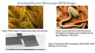
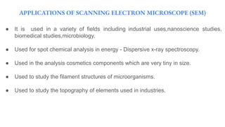
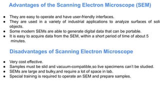
VIVEKANANDHA ARTS AND SCIENCE COLLEGE FOR WOMEN
VEERACHIPALAYAM - 6366007
SANKAGIRI, TAMIL NADU.
DEPARTMENT OF MICROBIOLOGY
SUBJECT INCHARGE
Dr.V.BHARATHI,M.Sc.,M.Phil.,Ph.D.
ASSISTANT PROFESSOR
DEPARTMENT OF MICROBIOLOGY
VIAAS, SANKAGIRI.
PRESENTED BY
DIVYAPRABHA K
I M.Sc MICROBIOLOGY
DEPARTMENT OF MICROBIOLOGY
VIAAS, SANKAGIRI
TOPIC : SCANNING ELECTRON MICROSCOPE
SUBJECT : GENERAL MICROBIOLOGY AND MICROBIAL DIVERSITY
INTRODUCTION
● The first Scanning Electron Microscope was initially made by Mafred
von Ardenne in 1937 with an aim to surpass the transmission electron
Microscope.
● He used high-resolution power to scan a small raster using a beam of
electrons that were focused on the raster.
● He also aimed at reducing the problems of chromatic aberrations
images produced by the Transmission electron Microscopes.
DEFINITION
● Scanning Electron Microscope (SEM) is a type of
electron microscope that scans surfaces of
microorganisms that uses a beam of electrons
moving at low energy to focus and scan specimens.
● The development of electron microscopes was due
to the inefficiency of the wavelength of light
microscopes. electron microscopes have very short
wavelengths in comparison to the light microscope
which enables better resolution power.
PRINCIPLES
● The scanning electron Microscope uses emitted electrons.
● The Scanning electron microscope works on the principle of applying
kinetic energy to produce signals on the interaction of the
electrons.
● The secondary electrons are emitted from the specimen play the
primary role of detecting the morphology and topography of the
specimen while the backscattered electrons show contrast in the
composition of the elements of the specimen.
Parts of a Scanning Electron Microscope (SEM)
The major components of the Scanning Electron Microscope include;
● Electron Source – This is where electrons are produced under thermal heat at a
voltage of 1-40kV.
● the electrons condense into a beam that is used for the creation of an image and
analysis.
● There are three types of electron sources that can be used i. e Tungsten filament,
Lanthanum hexaboride, and Field emission gun (FEG)
● Lenses – it has several condenser lenses that focus the beam of electrons from
the source through the column forming a narrow beam of electrons that form a spot
called a spot size.
● Scanning Coil – they are used to deflect the beam over the specimen surface.
● Detector – It’s made up of several detectors that are able to differentiate the
secondary electrons, backscattered electrons, and diffracted backscattered
electrons.
● The functioning of the detectors highly depends on the voltage speed, the density
of the specimen.
● The display device (data output devices)
● Power supply
● Vacuum system
PARTS OF SCANNING ELECTRON MICROSCOPE
Scanning Electron Microscope (SEM) Images
Figure: SEM image of Tradescantia pollen and stamens. Figure: Low-temperature scanning electron
micrograph of soybean cyst nematode and its
egg. Magnified 1,000 times.
Figure: Photoresist SEM micrograph (1995) SEM= DSM
982 Gemini from Zeiss.
APPLICATIONS OF SCANNING ELECTRON MICROSCOPE (SEM)
● It is used in a variety of fields including industrial uses,nanoscience studies,
biomedical studies,microbiology.
● Used for spot chemical analysis in energy - Dispersive x-ray spectroscopy.
● Used in the analysis cosmetics components which are very tiny in size.
● Used to study the filament structures of microorganisms.
● Used to study the topography of elements used in industries.
Advantages of the Scanning Electron Microscope (SEM)
● They are easy to operate and have user-friendly interfaces.
● They are used in a variety of industrial applications to analyze surfaces of solid
objects.
● Some modern SEMs are able to generate digital data that can be portable.
● It is easy to acquire data from the SEM, within a short period of time of about 5
minutes.
Disadvantages of Scanning Electron Microscope
● Very cost effective.
● Samples must be slid and vacuum-compatible,so live specimens can’t be studied.
● SEMs are large and bulky,and require a lot of space in lab.
● Special training is required to operate an SEM and prepare samples.
REFERENCES
● https://microbenotes.com/scanning-electron-microscope-sem/
● https://www.britannica.com/technology/scanning-electron-microscope
● https://blog.phenom-world.com/what-is-sem

General microbiology and microbial diversity - scanning electron microscope

  • 1.
    VIVEKANANDHA ARTS ANDSCIENCE COLLEGE FOR WOMEN VEERACHIPALAYAM - 6366007 SANKAGIRI, TAMIL NADU. DEPARTMENT OF MICROBIOLOGY SUBJECT INCHARGE Dr.V.BHARATHI,M.Sc.,M.Phil.,Ph.D. ASSISTANT PROFESSOR DEPARTMENT OF MICROBIOLOGY VIAAS, SANKAGIRI. PRESENTED BY DIVYAPRABHA K I M.Sc MICROBIOLOGY DEPARTMENT OF MICROBIOLOGY VIAAS, SANKAGIRI TOPIC : SCANNING ELECTRON MICROSCOPE SUBJECT : GENERAL MICROBIOLOGY AND MICROBIAL DIVERSITY
  • 2.
    INTRODUCTION ● The firstScanning Electron Microscope was initially made by Mafred von Ardenne in 1937 with an aim to surpass the transmission electron Microscope. ● He used high-resolution power to scan a small raster using a beam of electrons that were focused on the raster. ● He also aimed at reducing the problems of chromatic aberrations images produced by the Transmission electron Microscopes.
  • 3.
    DEFINITION ● Scanning ElectronMicroscope (SEM) is a type of electron microscope that scans surfaces of microorganisms that uses a beam of electrons moving at low energy to focus and scan specimens. ● The development of electron microscopes was due to the inefficiency of the wavelength of light microscopes. electron microscopes have very short wavelengths in comparison to the light microscope which enables better resolution power.
  • 4.
    PRINCIPLES ● The scanningelectron Microscope uses emitted electrons. ● The Scanning electron microscope works on the principle of applying kinetic energy to produce signals on the interaction of the electrons. ● The secondary electrons are emitted from the specimen play the primary role of detecting the morphology and topography of the specimen while the backscattered electrons show contrast in the composition of the elements of the specimen.
  • 5.
    Parts of aScanning Electron Microscope (SEM) The major components of the Scanning Electron Microscope include; ● Electron Source – This is where electrons are produced under thermal heat at a voltage of 1-40kV. ● the electrons condense into a beam that is used for the creation of an image and analysis. ● There are three types of electron sources that can be used i. e Tungsten filament, Lanthanum hexaboride, and Field emission gun (FEG) ● Lenses – it has several condenser lenses that focus the beam of electrons from the source through the column forming a narrow beam of electrons that form a spot called a spot size.
  • 6.
    ● Scanning Coil– they are used to deflect the beam over the specimen surface. ● Detector – It’s made up of several detectors that are able to differentiate the secondary electrons, backscattered electrons, and diffracted backscattered electrons. ● The functioning of the detectors highly depends on the voltage speed, the density of the specimen. ● The display device (data output devices) ● Power supply ● Vacuum system
  • 7.
    PARTS OF SCANNINGELECTRON MICROSCOPE
  • 8.
    Scanning Electron Microscope(SEM) Images Figure: SEM image of Tradescantia pollen and stamens. Figure: Low-temperature scanning electron micrograph of soybean cyst nematode and its egg. Magnified 1,000 times. Figure: Photoresist SEM micrograph (1995) SEM= DSM 982 Gemini from Zeiss.
  • 9.
    APPLICATIONS OF SCANNINGELECTRON MICROSCOPE (SEM) ● It is used in a variety of fields including industrial uses,nanoscience studies, biomedical studies,microbiology. ● Used for spot chemical analysis in energy - Dispersive x-ray spectroscopy. ● Used in the analysis cosmetics components which are very tiny in size. ● Used to study the filament structures of microorganisms. ● Used to study the topography of elements used in industries.
  • 10.
    Advantages of theScanning Electron Microscope (SEM) ● They are easy to operate and have user-friendly interfaces. ● They are used in a variety of industrial applications to analyze surfaces of solid objects. ● Some modern SEMs are able to generate digital data that can be portable. ● It is easy to acquire data from the SEM, within a short period of time of about 5 minutes. Disadvantages of Scanning Electron Microscope ● Very cost effective. ● Samples must be slid and vacuum-compatible,so live specimens can’t be studied. ● SEMs are large and bulky,and require a lot of space in lab. ● Special training is required to operate an SEM and prepare samples.
  • 11.