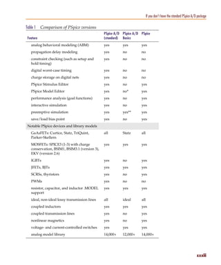
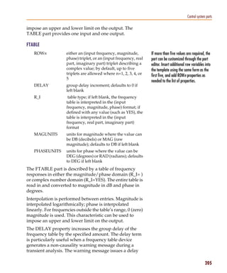
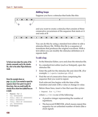
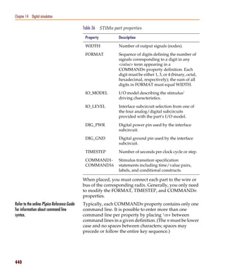
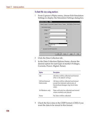
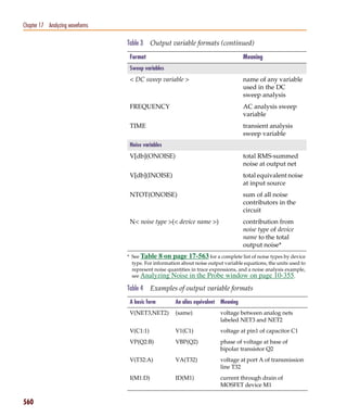
Downloaded 285 times


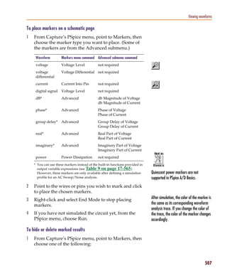
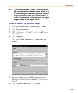
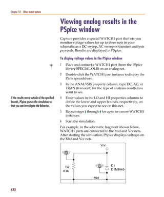
![Pspug.book Page 117 Tuesday, May 16, 2000 1:17 PM
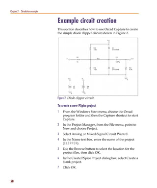
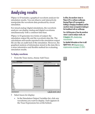
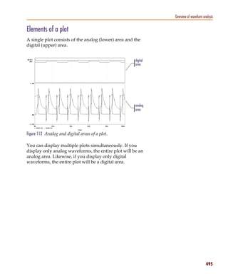
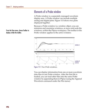
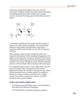
Defining stimuli
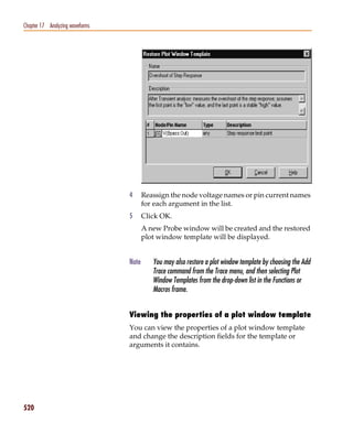
If you want to specify multiple stimulus types
If you want to run more than one analysis type, including
a transient analysis, then you need to use either of the
following:
• time-based stimulus parts with AC and DC properties
• VSRC or ISRC parts
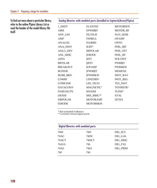
Using time-based stimulus parts with AC and DC properties
The time-based stimulus parts that you can use to define a
transient, DC, and/or AC input signal are listed below.
VEXP IEXP
VPULSE IPULSE
VPWL IPWL
VPWL_F_RE_FOREVER IPWL_F_RE_FOREVER
VPWL_F_N_TIMES IPWL_F_N_TIMES
VPWL_RE_FOREVER IPWL_RE_FOREVER
VPWL_RE_N_TIMES IPWL_RE_N_TIMES
VSFFM ISFFM
VSIN ISIN
In addition to the transient properties, each of these parts
also has a DC and AC property. When you use one of For the meaning of transient source
these parts, you must define all of the transient properties. properties, refer to the I/V (independent
However, it is common to leave DC and/or AC undefined current and voltage source) device type
(blank). When you give them a value, the syntax you need syntax in the Analog Devices chapter in the
to use is as follows. online PSpice Reference Guide.
This property... Has this syntax...
DC DC_value[units]
AC magnitude_value[units] [phase_value]
117](https://image.slidesharecdn.com/spice-130129163004-phpapp01/85/PSpice-117-320.jpg)
![Pspug.book Page 118 Tuesday, May 16, 2000 1:17 PM
Chapter 3 Preparing a design for simulation
Using VSRC or ISRC parts
The VSRC and ISRC parts have one property for each
analysis type: DC, AC, and TRAN. You can set any or all
of them using PSpice netlist syntax. When you give them
a value, the syntax you need to use is as follows.
This property... Has this syntax...
DC DC_value[units]
AC magnitude_value[units] [phase_value]
For the syntax and meaning of transient TRAN time-based_type (parameters)
source specifications, refer to the I/V where time-based_type is EXP, PULSE, PWL,
(independent current and voltage source) SFFM, or SIN, and the parameters depend on
device type in the Analog Devices chapter the time-based_type.
in the online PSpice Reference Guide.
Note Orcad recommends that if you are running only a transient
analysis, use a VSTIM or ISTIM part if you have the standard
package, or one of the other time-based source parts that has
properties specific for a waveform shape.
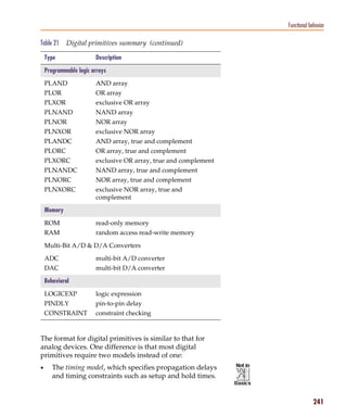
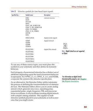
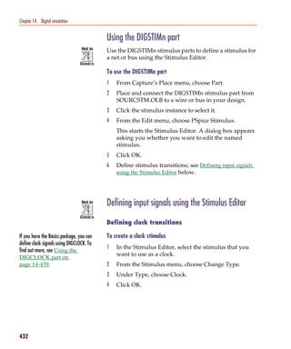
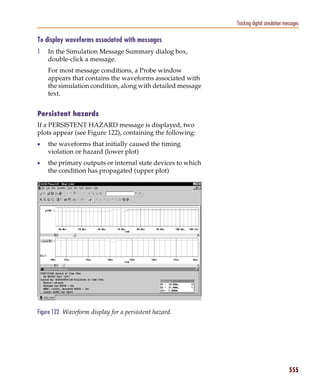
Digital stimuli
If you want this kind of input... Use this part....
You can use the DIGSTIM part to define For transient analyses
both 1-bit signal or bus (n width) input signal or bus (n width) DIGSTIMn*
signals using the Stimulus Editor.
clock signal DIGCLOCK
See Defining a digital stimulus on
1-bit signal STIM1
page 14-431 to find out more about:
4-bit bus STIM4
• all of these source parts, and
8-bit bus STIM8
• how to use the Stimulus Editor to
specify DIGSTIMn (DIGSTIM1, 16-bit bus STIM16
DIGSTIM4, etc.) part. file-based signal or bus (n width) FILESTIMn
* The DIGSTIM part requires the Stimulus Editor to define the input signal;
these parts are not available in Basics+.
118](https://image.slidesharecdn.com/spice-130129163004-phpapp01/85/PSpice-118-320.jpg)


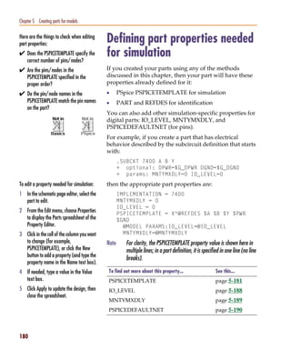
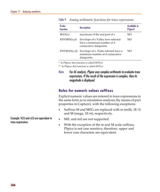
![Pspug.book Page 181 Tuesday, May 16, 2000 1:17 PM
Defining part properties needed for simulation
PSPICETEMPLATE
The PSPICETEMPLATE property defines the PSpice Caution—Creating parts
syntax for the part’s netlist entry. When creating a netlist, not intended for simulation
Capture substitutes actual values from the circuit into the Some part libraries contain parts designed
appropriate places in the PSPICETEMPLATE syntax, then only for board layout; PSpice cannot
saves the translated statement to the netlist file. simulate these parts. This means they do
Any part that you want to simulate must have a defined not have PSPICETEMPLATE properties or
PSPICETEMPLATE property. These rules apply: that the PSPICETEMPLATE property value is
blank.
• The pin names specified in the PSPICETEMPLATE
property must match the pin names on the part.
• The number and order of the pins listed in the
PSPICETEMPLATE property must match those for
the associated .MODEL or .SUBCKT definition
referenced for simulation.
• The first character in a PSPICETEMPLATE must be a
PSpice device letter appropriate for the part (such as Q
for a bipolar transistor).
PSPICETEMPLATE syntax
The PSPICETEMPLATE contains:
• regular characters that the schematic page editor
interprets verbatim
• property names and control characters that the schematic
page editor translates
Regular characters in templates
Regular characters include the following:
• alphanumerics
• any keyboard part except the special syntactical parts
used with properties (@ & ? ~ #).
• white space
An identifier is a collection of regular characters of the
form:
alphabetic character [any other regular character]*.
181](https://image.slidesharecdn.com/spice-130129163004-phpapp01/85/PSpice-181-320.jpg)
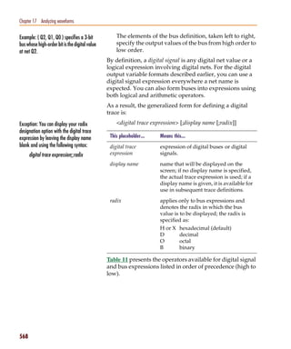
![Pspug.book Page 182 Tuesday, May 16, 2000 1:17 PM
Chapter 5 Creating parts for models
Property names in templates
Property names are preceded by a special character as
follows:
[ @ | ? | ~ | # | & ]<identifier>
The schematic page editor processes the property
according to the special character as shown in the
following table.
This syntax...* Is replaced with this...
@<id> Value of <id>. Error if no <id> attribute or
if no value assigned.
&<id> Value of <id> if <id> is defined.
?<id>s...s Text between s...s separators if <id> is
defined.
?<id>s...ss...s Text between the first s...s separators if
<id> is defined, else the second s...s clause.
~<id>s...s Text between s...s separators if <id> is
undefined.
~<id> s...ss...s Text between the first s...s separators if
<id> is undefined, else the second s...s
clause.
#<id>s...s Text between s...s separators if <id> is
defined, but delete rest of template if <id>
is undefined.
* s is a separator character
Example: The template fragment Separator characters include commas (,), periods (.),
?G|G=@G||G=1000| uses the vertical semi-colons (;), forward slashes (/), and vertical
bar as the separator between the bars ( | ). You must always use the same character to
if-then-else parts of this conditional clause. specify an opening-closing pair of separators.
If G has a value, then this fragment
Note You can use different separator characters to nest conditional
translates to G=<G property
value>. Otherwise, this fragment
property clauses.
translates to G=1000.
182](https://image.slidesharecdn.com/spice-130129163004-phpapp01/85/PSpice-182-320.jpg)

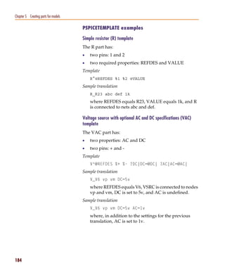
![Pspug.book Page 186 Tuesday, May 16, 2000 1:17 PM
Chapter 5 Creating parts for models
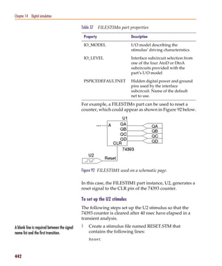
Digital stimulus parts with variable width pins template
For a digital stimulus device template (such as that for a
DIGSTIM part), a pin name can be preceded by a
* character. This signifies that the pin can be connected to
a bus and the width of the pin is set to be equal to the
width of the bus.
Note For clarity, the PSPICETEMPLATE Template
property value is shown here in multiple U^@REFDES STIM(%#PIN, 0) %*PIN
lines; in a part definition, it is specified in n+ STIMULUS=@STIMULUS
one line (no line breaks).
where #PIN refers to a variable width pin.
Sample translation
U_U1 STIM(4,0) 5PIN1 %PIN2 %PIN3 %PIN4
+ STIMULUS=mystim
where the stimulus is connected to a four-input bus,
a[0-3].
Pin callout in subcircuit templates
To find out how to define subcircuits, refer The number and sequence of pins named in a template for
to the .SUBCKT command in the online a subcircuit must agree with the definition of the
PSpice Reference Guide. subcircuit itself—that is, the node names listed in the
.SUBCKT statement, which heads the definition of a
subcircuit. These are the pinouts of the subcircuit.
Example: Consider the following first line of a
(hypothetical) subcircuit definition:
.SUBCKT SAMPLE 10 3 27 2
The four numbers following the name SAMPLE—10, 3,
27, and 2—are the node names for this subcircuit’s
pinouts.
Now suppose that the part definition shows four pins:
IN+ OUT+ IN- OUT-
The number of pins on the part equals the number of
nodes in the subcircuit definition.
186](https://image.slidesharecdn.com/spice-130129163004-phpapp01/85/PSpice-186-320.jpg)


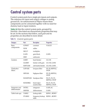
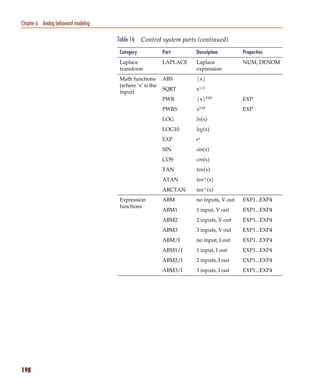


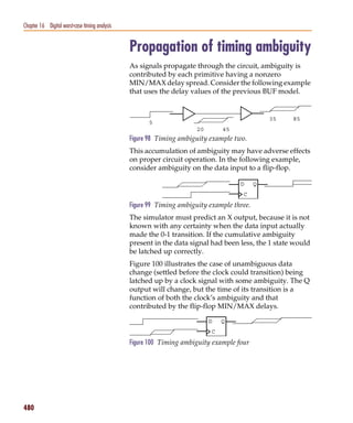
![Pspug.book Page 209 Tuesday, May 16, 2000 1:17 PM
Control system parts
159 Hz. There is also a phase shift centered around 159 Hz.
In other words, the gain has both a real and an imaginary
component. For transient analysis, the output is the
convolution of the input waveform with the impulse
response of 1/(1+.001·s). The impulse response is a
decaying exponential with a time constant of 1
millisecond. This means that the output is the “lossy
integral” of the input, where the loss has a time constant
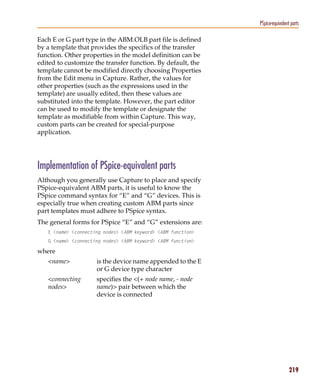
of 1 millisecond. The LAPLACE part shown in Figure 39
could be used for this purpose.
The transfer function is the Laplace transform
(1/[1+.001*s]). This LAPLACE part is characterized by the Figure 39 LAPLACE part example one.
following properties:
NUM = 1
DENOM = 1 + .001*s
The gain and phase characteristics are shown in Figure 40.
Figure 40 Viewing gain and phase characteristics of a lossy
integrator.
This produces a PSpice netlist declaration like this:
ERC 5 0 LAPLACE {V(10)} = {1/(1+.001*s)}
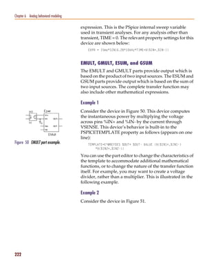
Example two
The input is V(10). The output is a current applied
between nets 5 and 0. The Laplace transform describes a Figure 41 LAPLACE part example two.
209](https://image.slidesharecdn.com/spice-130129163004-phpapp01/85/PSpice-209-320.jpg)


![Pspug.book Page 215 Tuesday, May 16, 2000 1:17 PM
Control system parts
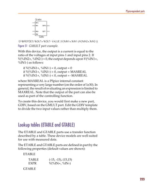
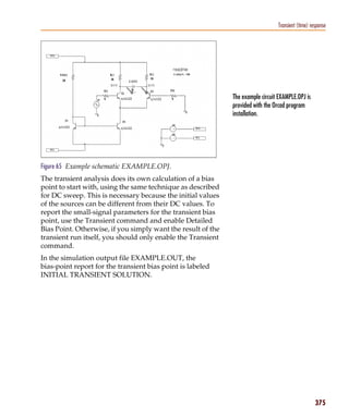
An instantaneous device example: modeling a
triode
This section provides an example of using various ABM
parts to model a triode vacuum tube. The schematic of the
triode subcircuit is shown in Figure 46.
Figure 46 Triode circuit.
Assumptions: In its main operating region, the triode’s
current is proportional to the 3/2 power of a linear
combination of the grid and anode voltages:
ianode = k0*(vg + k1*va)1.5
For a typical triode, k0 = 200e-6 and k1 = 0.12.
Looking at the upper left-hand portion of the schematic,
notice the a general-purpose ABM part used to take the
input voltages from anode, grid, and cathode. Assume the
following associations:
• V(anode) is associated with V(%IN1)
• V(grid) is associated with V(%IN2)
• V(cathode) is associated with V(%IN3)
The expression property EXP1 then represents V(grid,
cathode) and the expression property EXP2 represents
0.12[V(anode, cathode)]. When the template substitution
is performed, the resulting VALUE is equivalent to the
following:
V = V(grid, cathode) + 0.12*V(anode, cathode)
215](https://image.slidesharecdn.com/spice-130129163004-phpapp01/85/PSpice-215-320.jpg)


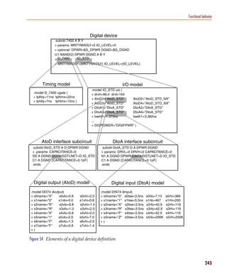
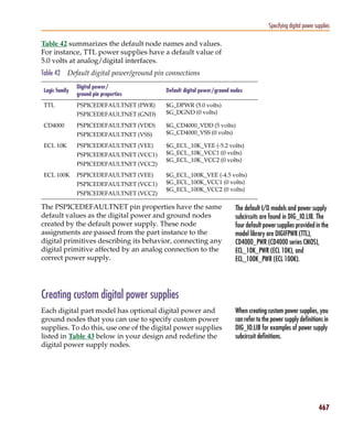
![Pspug.book Page 242 Tuesday, May 16, 2000 1:17 PM
Chapter 7 Digital device modeling
• The I/O model, which specifies information specific to
the device’s input/output characteristics.
The reason for having two models is that, while timing
information is specific to a device, the input/output
characteristics are specific to a whole logic family. Thus,
many devices in the same family reference the same I/O
model, but each device has its own timing model.
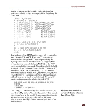
Figure 54 presents an overview of a digital device
definition in terms of its primitives and underlying model
attributes. These models are discussed further on Timing
For specific information on each primitive model on page 7-247 and Input/Output model on page 7-253.
type see the online PSpice Reference Guide.
Note that some digital primitives, such as Digital primitive syntax
pullups, do not have Timing models. See
Timing model on page 7-247 for The general digital primitive format is shown below.
more information. U<name> <primitive type> [( <parameter value>* )]
+ <digital power node> <digital ground node>
+ <node>*
+ <Timing Model name> <I/O Model name>
+ [MNTYMXDLY=<delay select value>]
+ [IO_LEVEL=<interface subckt select value>]
where
<primitive type> [( <parameter value>* )]
is the type of digital device, such as NAND, JKFF, or INV.
It is followed by zero or more parameters specific to the
primitive type, such as number of inputs. The number and
meaning of the parameters depends on the primitive type.
<digital power node> <digital ground node>
are the nodes used by the interface subcircuits which
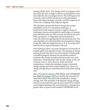
connect analog nodes to digital nodes or vice versa.
<node>*
is one or more input and output nodes. The number of
nodes depends on the primitive type and its
parameters. Analog devices, digital devices, or both
may be connected to a node. If a node has both analog
and digital connections, then PSpice A/D
242](https://image.slidesharecdn.com/spice-130129163004-phpapp01/85/PSpice-242-320.jpg)


![Pspug.book Page 253 Tuesday, May 16, 2000 1:17 PM
Input/Output characteristics
Input/Output characteristics
A digital device model’s input/output characteristics are
defined by the I/O model that it references. Some
characteristics, such as output drive resistance and
loading capacitances, apply to digital simulation. Others,
such as the interface subcircuits and the power supplies,
apply only to mixed analog/digital simulation.
This section describes in detail:
• the I/O model
• the relationship between drive resistances and output
strengths
• charge storage on digital nets
• the format of the interface subcircuits
Input/Output model
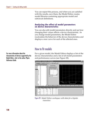
I/O models are common to entire logic families. For
example, in the model libraries, there are only four I/O
models for the entire 74LS family: IO_LS, for standard
inputs and outputs; IO_LS_OC, for standard inputs and
open-collector outputs; IO_LS_ST, for Schmitt trigger
inputs and standard outputs; and IO_LS_OC_ST, for
Schmitt trigger inputs and open-collector outputs. In
contrast, timing models are unique to each device.
I/O models are specified as
.MODEL <I/O model name> UIO [model parameters]*
where valid model parameters are described in Table 22.
253](https://image.slidesharecdn.com/spice-130129163004-phpapp01/85/PSpice-253-320.jpg)


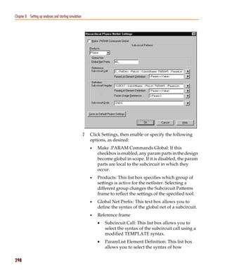
 (1)
where <out id > is:
<net id> or <pin id> (2)
<net id> is a fully qualified net name (3)
<pin id> is <fully qualified device name>:<pin name> (4)
A fully qualified net name (as referred to in line 3 above)
is formed by prefixing the visible net name (from a label
applied to one of the segments of a wire or bus, or an
offpage port connected to the net) with the full
hierarchical path, separated by periods. At the top level of
hierarchy, this is just the visible name.
A fully qualified device name (from line 4 above) is
distinguished by specifying the full hierarchical path
followed by the device’s part reference, separated by
period characters. For example, a resistor with part
reference R34 inside part Y1 placed on a top-level
286](https://image.slidesharecdn.com/spice-130129163004-phpapp01/85/PSpice-286-320.jpg)

where <out device> is a fully qualified device name.
Modifiers
The basic syntax for output variables can be modified to
indicate terminals of semiconductors and AC
specifications. The modifiers come before <out id> or
<out device>. Or, when specifying terminals (such as
source or drain), the modifier is the pin name contained in
<out id>, or is appended to <out device> separated by a
colon.
Modifiers can be specified as follows:
• For voltage:
v[AC suffix](<out id>[, out id])
v[terminal]*(<out device>)
• For current:
i[AC suffix](<out device>[:terminal])
i[terminal][AC suffix](<out device>])
where
terminal specifies one or two terminals for devices
with more than two terminals, such as D
(drain), G (gate), S (source)
287](https://image.slidesharecdn.com/spice-130129163004-phpapp01/85/PSpice-287-320.jpg)
 voltage at out id
V[ac](< +out id >,< - out id >) voltage across + and -
out id’s
V[ac](< 2-terminal device out id >) voltage at a 2-terminal
device out id
V[ac](< 3 or 4-terminal device out id >) or voltage at
V<x>[ac](< 3 or 4-terminal out device >) non-grounded terminal
x of a 3 or 4-terminal
device
V<x><y>[ac](< 3 or 4-terminal out device >) voltage across terminals
x and y of a
3 or 4-terminal device
V[ac](< transmission line out id >) or voltage at one end z of a
V<z>[ac](< transmission line out device >) transmission line device
I[ac](< 3 or 4-terminal out device >:<x>) or current through
I<x>[ac](< 3 or 4-terminal out device >) non-grounded terminal
x of a 3 or 4-terminal out
device
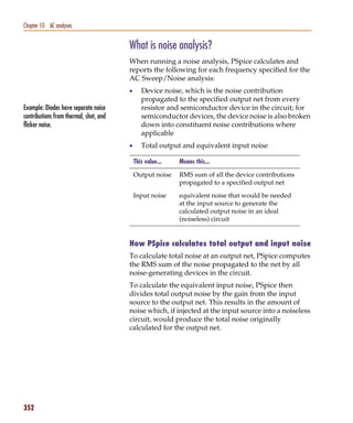
I[ac](< transmission line out device >:<z>) or current through one end
I<z>[ac](< 3 or 4-terminal out device >) z of a transmission line
out device
< DC sweep variable > voltage or current
source name
288](https://image.slidesharecdn.com/spice-130129163004-phpapp01/85/PSpice-288-320.jpg)


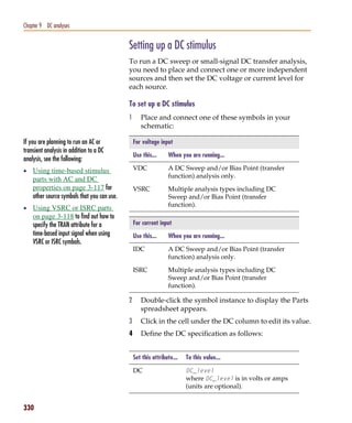


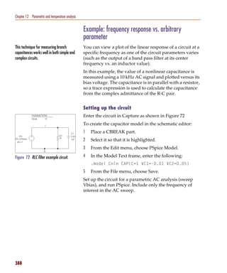
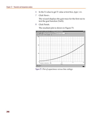
![Pspug.book Page 344 Tuesday, May 16, 2000 1:17 PM
Chapter 10 AC analyses
2 Double-click the symbol instance to display the Parts
spreadsheet.
3 Click in the cell under the appropriate property
column to edit its value. Depending on the source
symbol that you placed, define the AC specification as
follows:
For VAC or IAC
Set this property... To this value...
ACMAG AC magnitude in volts (for VAC) or
amps (for IAC); units are optional.
ACPHASE Optional AC phase in degrees.
For VSRC or ISRC
Set this property... To this value...
If you are also planning to run a transient AC Magnitude_value [phase_value]
analysis, see Using VSRC or ISRC where magnitude_value is in volts or
parts on page 3-118 to find out how amps (units are optional) and the
to specify the TRAN property. optional phase_value is in degrees.
344](https://image.slidesharecdn.com/spice-130129163004-phpapp01/85/PSpice-344-320.jpg)


![Pspug.book Page 354 Tuesday, May 16, 2000 1:17 PM
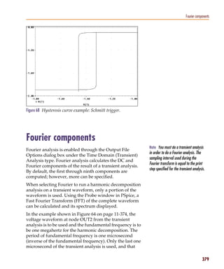
Chapter 10 AC analyses
6 Enter the noise analysis parameters as follows:
In this text box... Type this...
To find out more about valid syntax, see Output Voltage A voltage output variable of the
Output variables on page 8-286. form V(node, [node]) where you
want the total output noise
calculated.
I/V Source The name of an independent current
or voltage source where you want
the equivalent input noise
calculated.
Note If the source is in a lower level of
a hierarchical schematic, separate the
Example: U1.V2 names of the hierarchical devices with
periods (.).
Note In the Probe window, you can view Interval An integer n designating that at
the device noise contributions at every every nth frequency, you want to see
frequency specified in the AC sweep. The a table printed in the PSpice output
Interval parameter has no effect on what file (.out) showing the individual
PSpice writes to the Probe data file. contributions of all of the circuit’s
noise generators to the total noise.
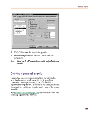
7 Click OK to save the simulation profile.
354](https://image.slidesharecdn.com/spice-130129163004-phpapp01/85/PSpice-354-320.jpg)


![Pspug.book Page 420 Tuesday, May 16, 2000 1:17 PM
Chapter 13 Monte Carlo and sensitivity/worst-case analyses
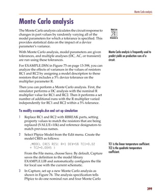
Worst-case analysis example
The schematic shown in Figure 85 is for an amplifier
circuit that is a biased BJT. This circuit is used to
demonstrate how a simple worst-case analysis works. It
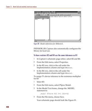
also shows how non-monotonic dependence of the output
on a single parameter can adversely affect the worst-case
analysis.
Because an AC (small-signal) analysis is being performed,
setting the input to unity means that the output,
Vm([OUT]), is the magnitude of the gain of the amplifier.
The only variable declared in this circuit is the resistance
of Rb2. Because the value of Rb2 determines the bias on the
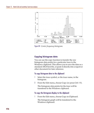
BJT, it also affects the amplifier’s gain.
Figure 85 Simple biased BJT amplifier.
Figure 86 is the circuit file used to run one of the
following:
• a parametric analysis (.STEP, shown enabled in the
circuit file) that sets the value of resistor Rb2 by
stepping model parameter R through values spanning
the specified DEV tolerance range, or
• a worst-case analysis (shown disabled in the circuit
file) that allows PSpice to determine the worst-case
value for parameter R based upon a sensitivity
analysis.
420](https://image.slidesharecdn.com/spice-130129163004-phpapp01/85/PSpice-420-320.jpg)
![Pspug.book Page 421 Tuesday, May 16, 2000 1:17 PM
Worst-case analysis
Only one of these analyses can run in any given
simulation.
Note The AC and worst-case analysis specifications (.AC and .WC
statements) are written so that the worst-case analysis tries to
minimize Vm([OUT]) at 100 kHz.
The netlist and circuit file in Figure 86 are set up to run
either a parametric (.STEP) or worst-case (.WC) analysis of
the specified AC analysis. These simulations demonstrate
the conditions under which worst-case analysis works
well and those that can produce misleading results when
* Worst-case analysis comparing monotonic and non-monotonic
* output with a variable parameter
.lib
***** Input signal and blocking capacitor *****
Vin In 0 ac 1
Cin In B 1u
***** "Amplifier" *****
* gain increases with small increase in Rb2, but
* device saturates if Rb2 is maximized.
Vcc Vcc 0 10
Rc Vcc C 1k
Q1 C B 0 Q2N2222
Rb1 Vcc B 10k
Rb2 B 0 Rbmod 720
.model Rbmod res(R=1 dev 5%) ; WC analysis results
; are correct
* .model Rbmod res(R=1.1 dev 5%) ; WC analysis misled
; by sensitivity
***** Load and blocking capacitor *****
CoutC Out 1u
Rl Out 0 1k
* Run with either the .STEP or the .WC, but not both.
* This circuit file is currently set up to run the .STEP
* (.WC is commented out)
**** Parametric Sweep—providing plot of Vm([OUT]) vs. Rb2 ****
.STEP Res Rbmod(R) 0.8 1.2 10m
***** Worst-case analysis *****
* run once for each of the .model definitions stated above)
* WC AC Vm([Out]) min range 99k 101k list output all
.AC Lin 3 90k 110k
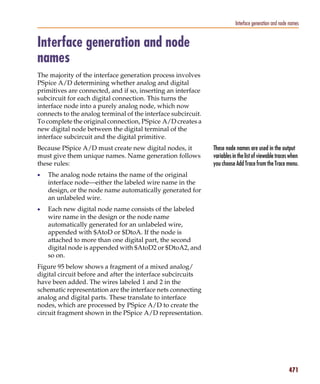
.probe
.end
Figure 86 Amplifier netlist and circuit file.
421](https://image.slidesharecdn.com/spice-130129163004-phpapp01/85/PSpice-421-320.jpg)
![Pspug.book Page 422 Tuesday, May 16, 2000 1:17 PM
Chapter 13 Monte Carlo and sensitivity/worst-case analyses
output is not monotonic with a variable parameter (see
Figure 88 and Figure 89)
For demonstration, the parametric analysis is run first,
generating the curve shown in Figure 88 and Figure 89.
This curve, derived using the YatX goal function shown in
Figure 87 illustrates the non-monotonic dependence of
gain on Rb2.
YatX(1, X_value)=y1{1|sfxv(X_value)!1;}
Figure 87 YatX Goal Function.
To do this yourself, place the goal function definition in a
PROBE.GF file in the circuit directory. Then start PSpice,
load all of the AC sweeps, set up the X axis for
performance analysis, and add the following trace:
Note The YatX goal function is used on the YatX(Vm([OUT]),100k)
simulation results for the parametric sweep
Next, the parametric analysis is commented out and the
(.STEP) defined in Figure 86. The resulting
worst-case analysis is enabled. Two runs are made using
curves are shown in Figure 88 and
the two versions of the Rbmod .MODEL statement shown
Figure 89.
in the circuit file. The model parameter, R, is a multiplier
which is used to scale the nominal value of any resistor
referencing the Rbmod model (Rb2 in this case).
The first .MODEL statement leaves the nominal value of
Rb2 at 720 ohms. The sensitivity analysis increments R by
a small amount and checks its effect on Vm([OUT]). This
slight increase in R causes an increase in the base bias
voltage of the BJT, and increases the amplifier’s gain,
Vm([OUT]). The worst-case analysis correctly sets R to its
minimum value for the lowest possible Vm([OUT]) (see
Figure 88).
422](https://image.slidesharecdn.com/spice-130129163004-phpapp01/85/PSpice-422-320.jpg)


This document is the user guide for PSpice A/D, PSpice A/D Basics, and PSpice. It provides an overview of the software and describes how to use it. The guide covers topics such as simulations that can be run, files needed for simulation, examples of different types of analyses like DC sweep and transient analyses, and how to prepare a design for simulation. It also provides checklists and information on using parts, parameters, and expressions to set up simulations.