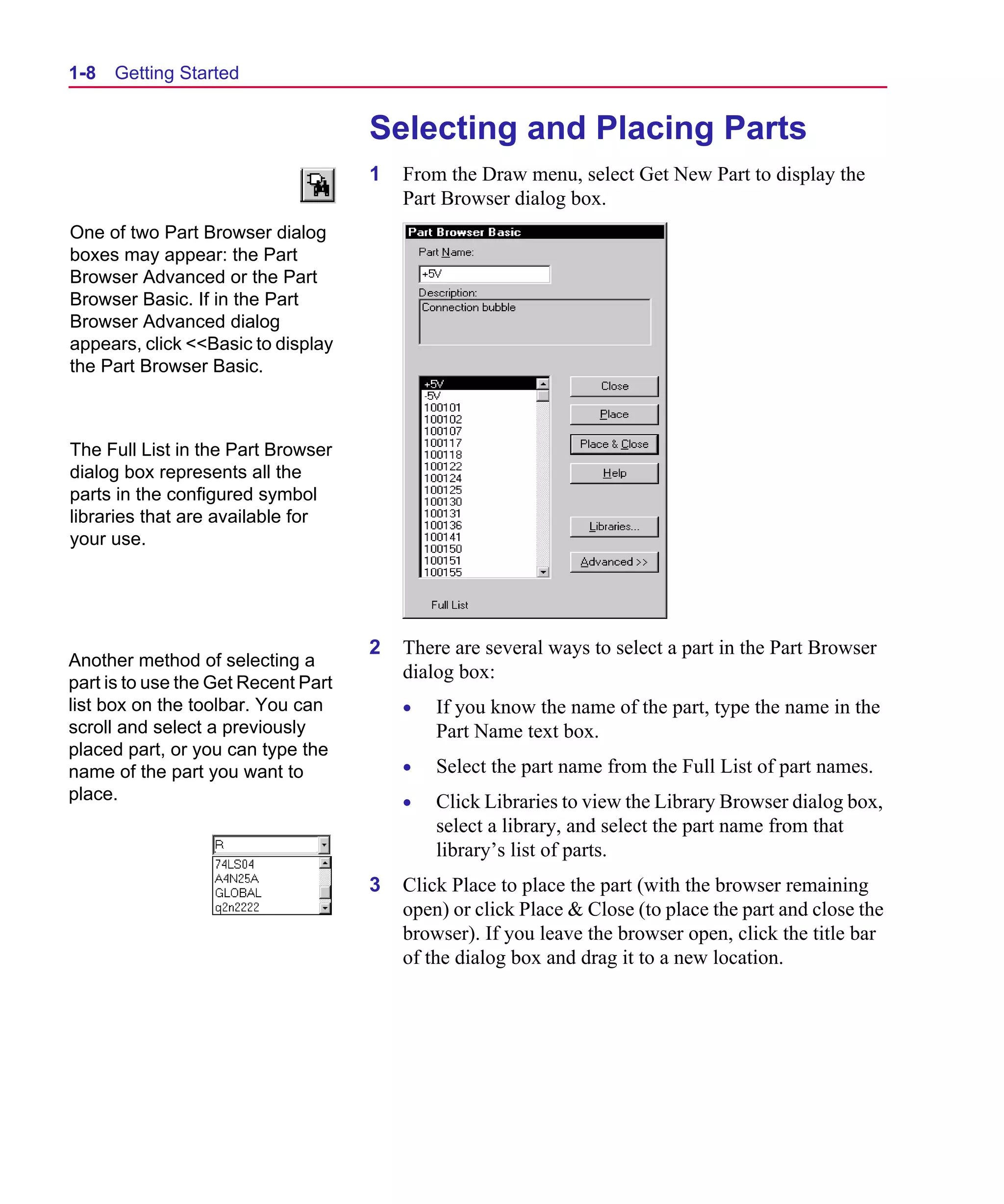
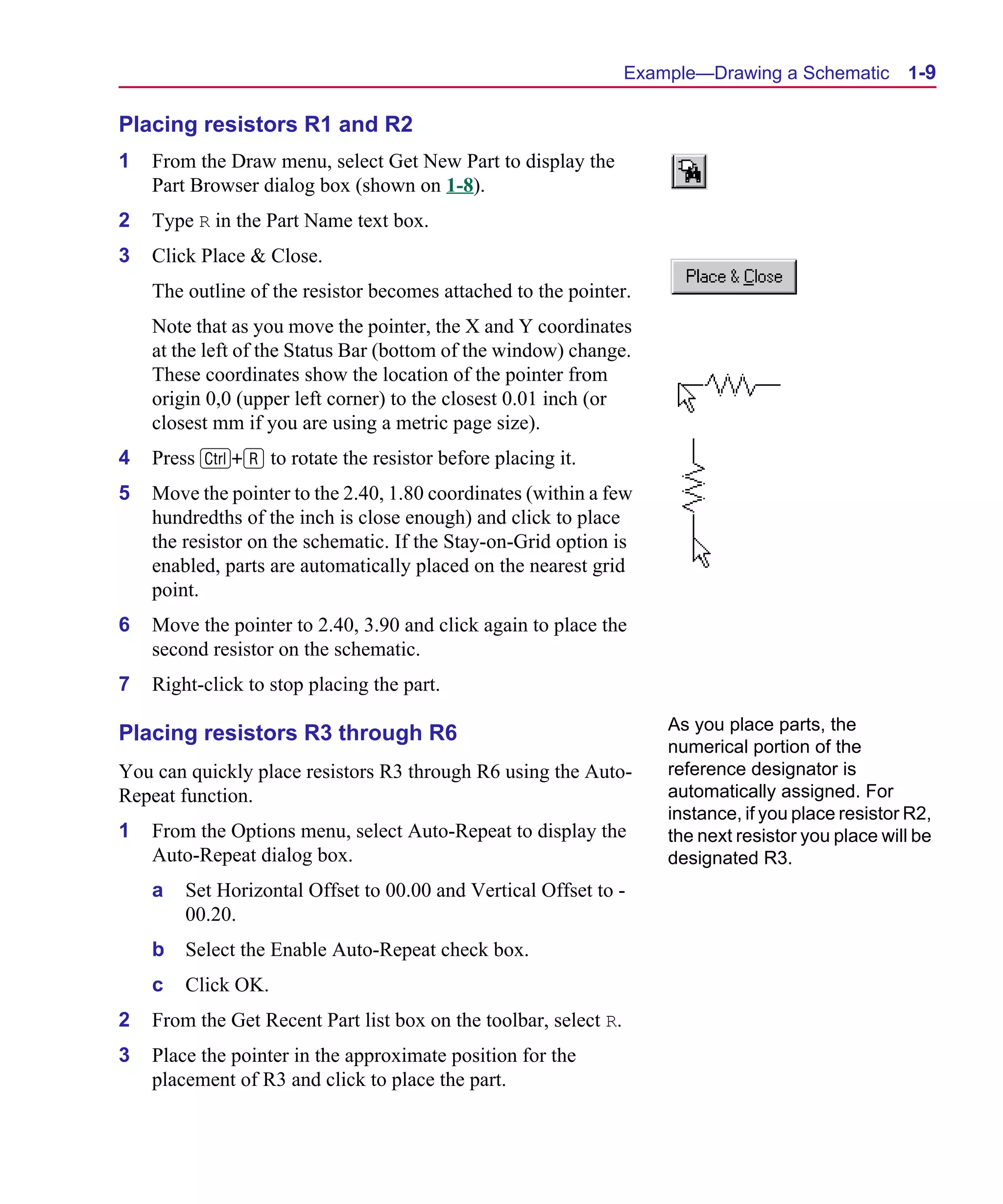
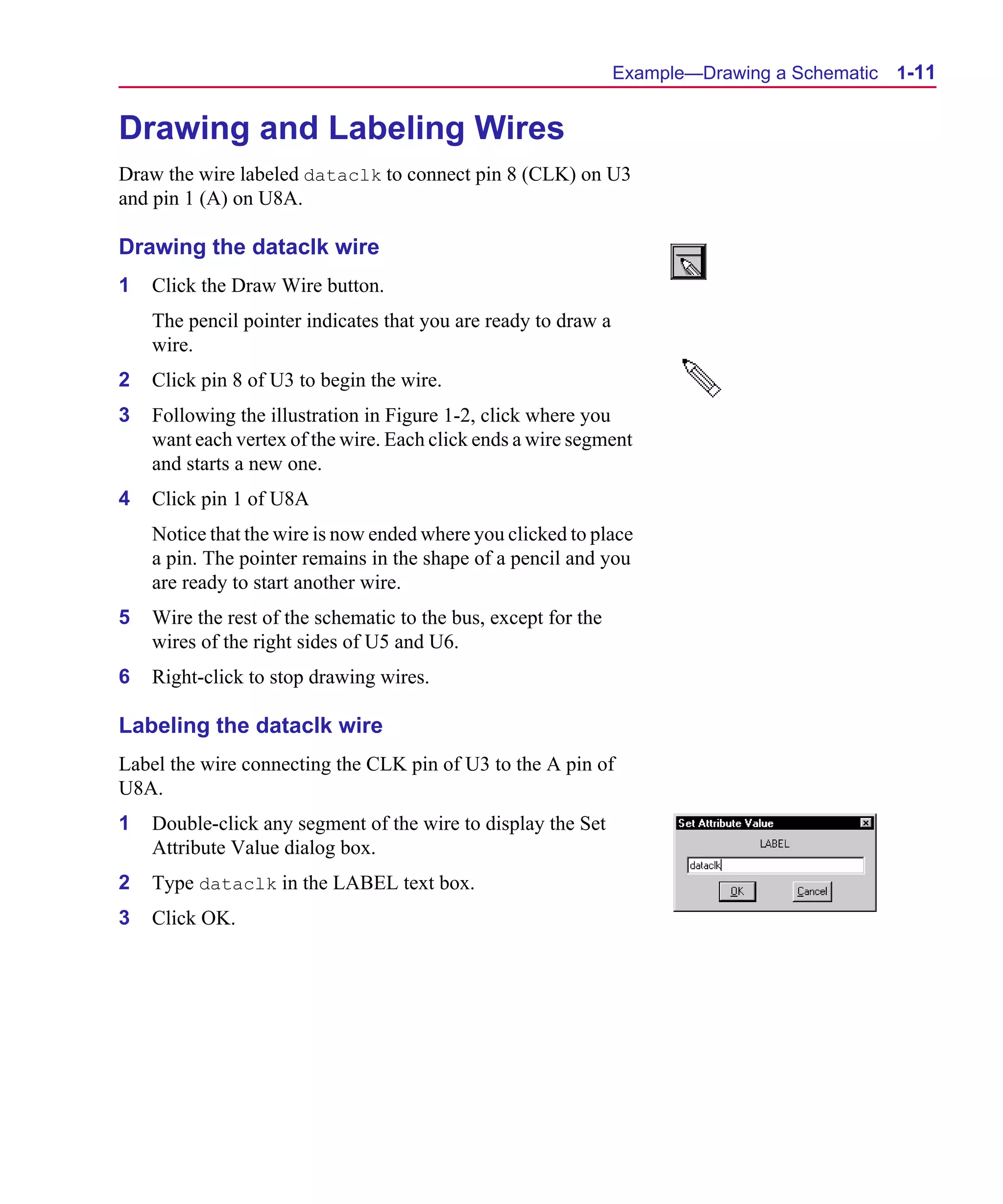
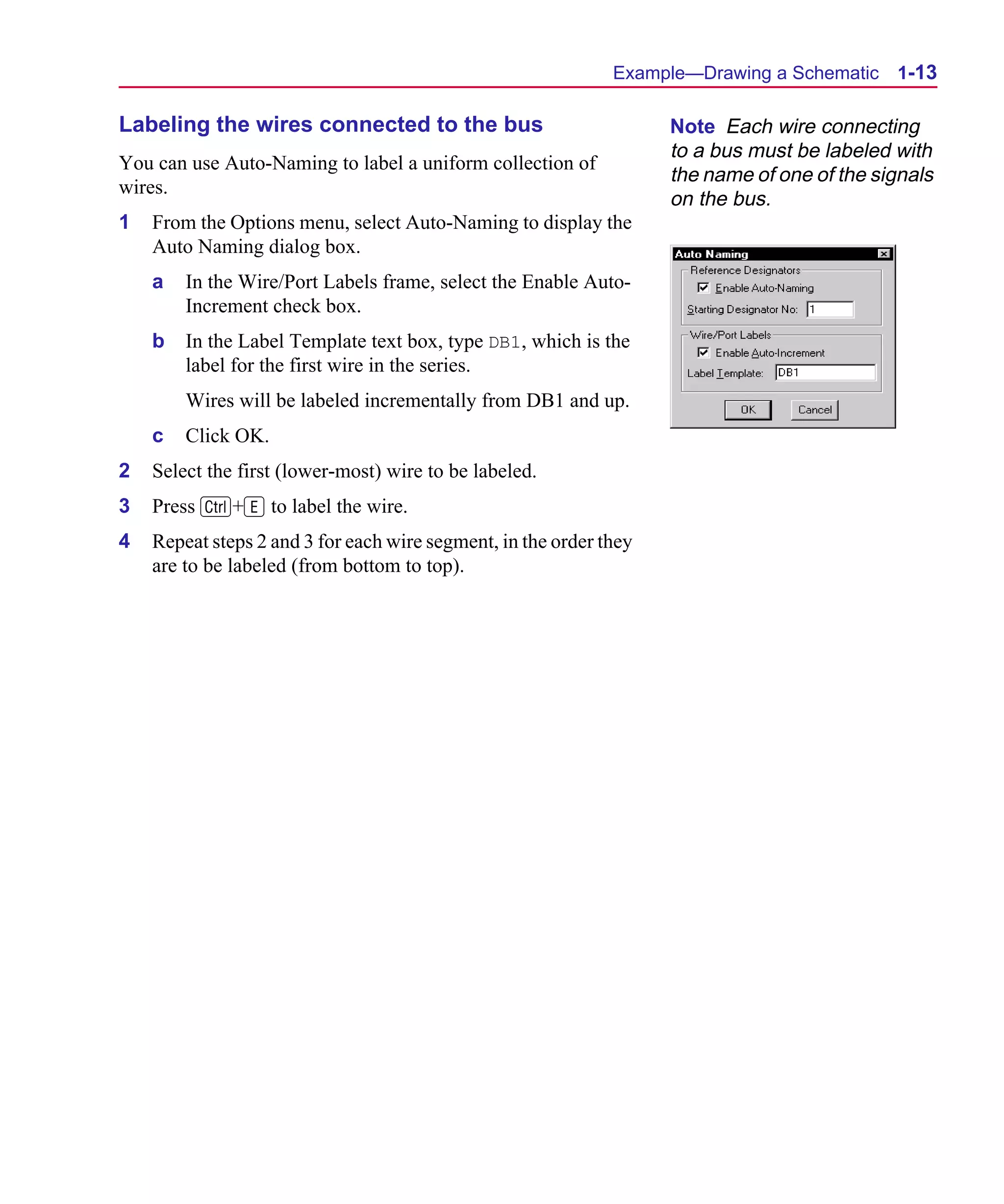
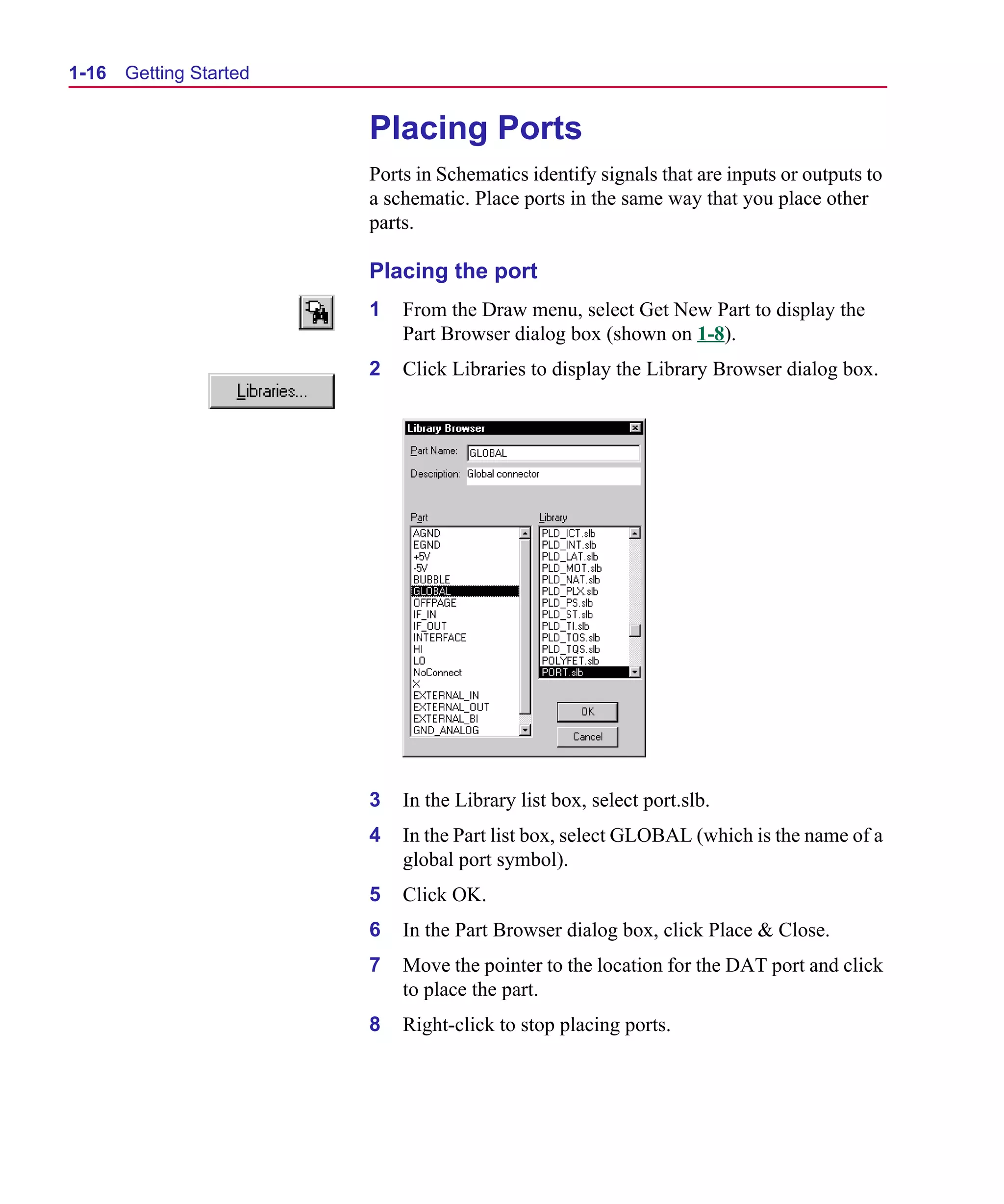
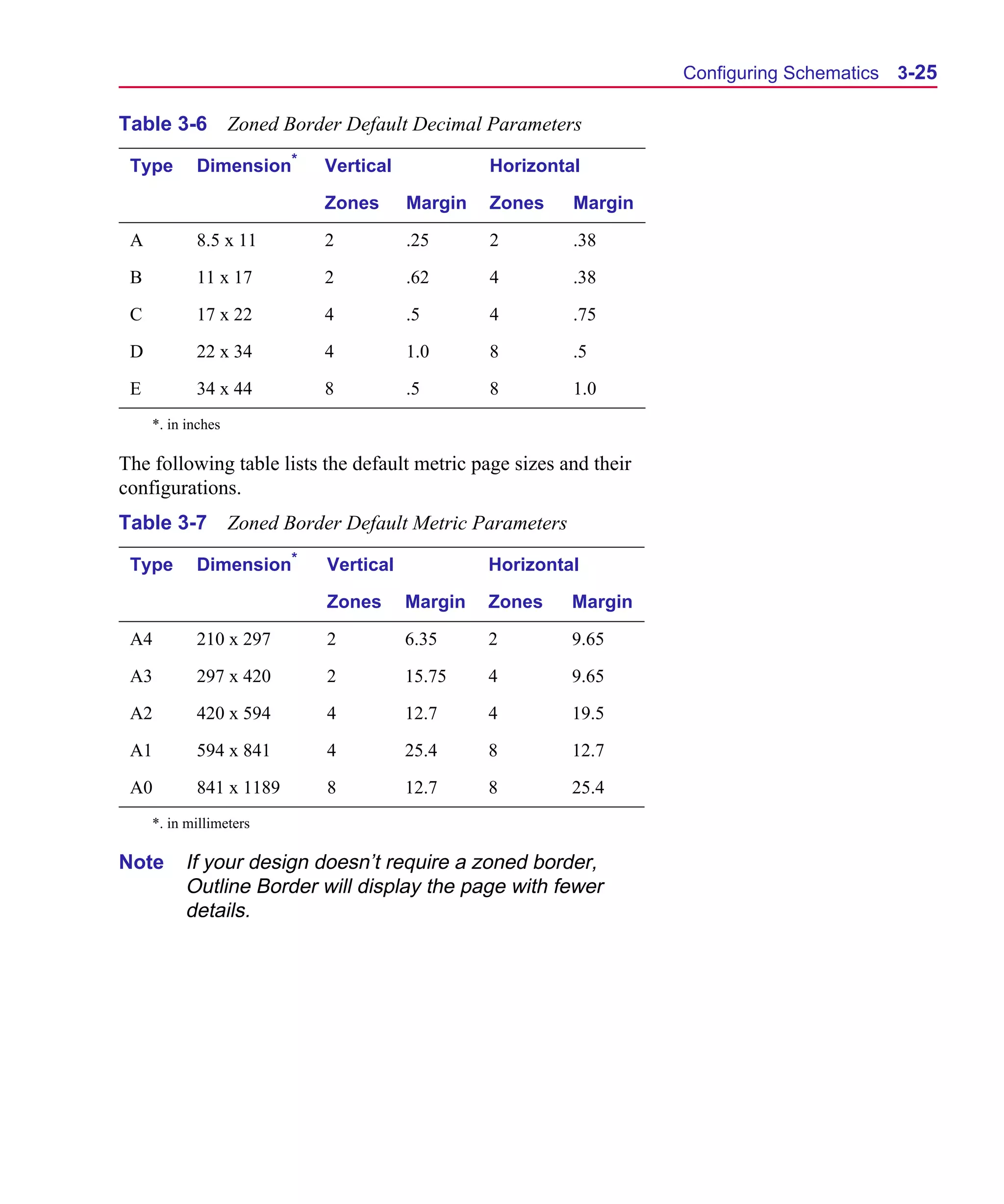
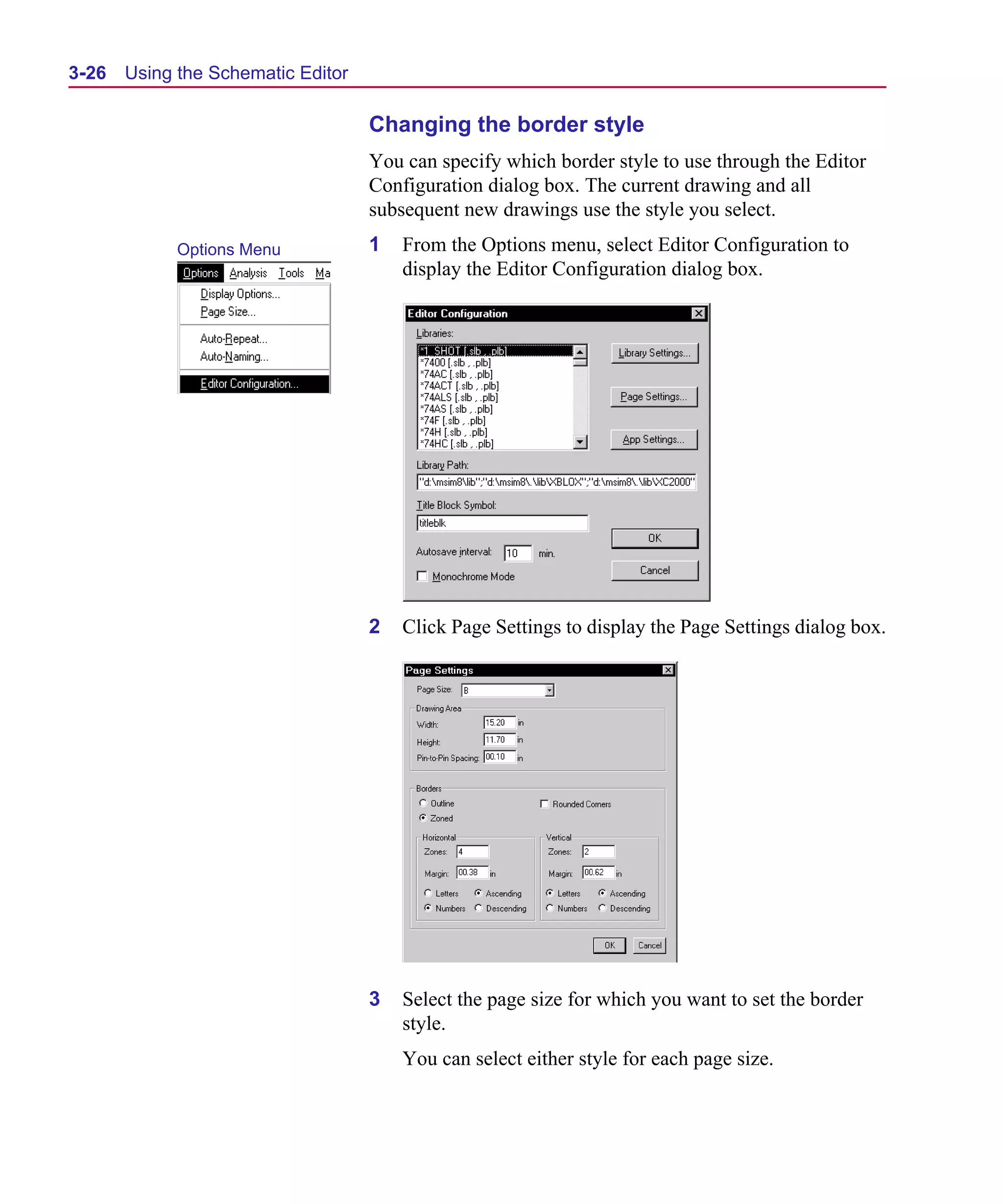
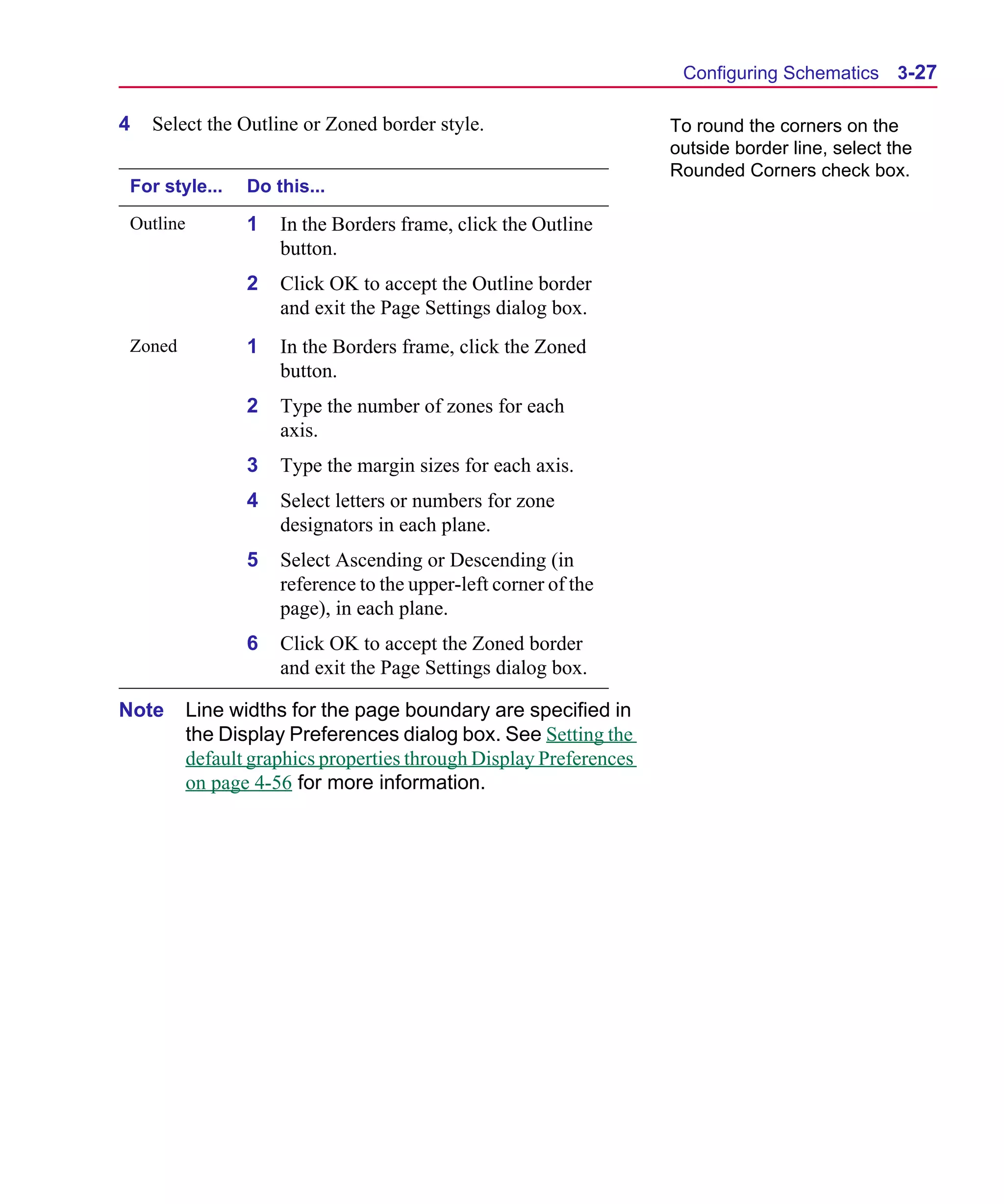
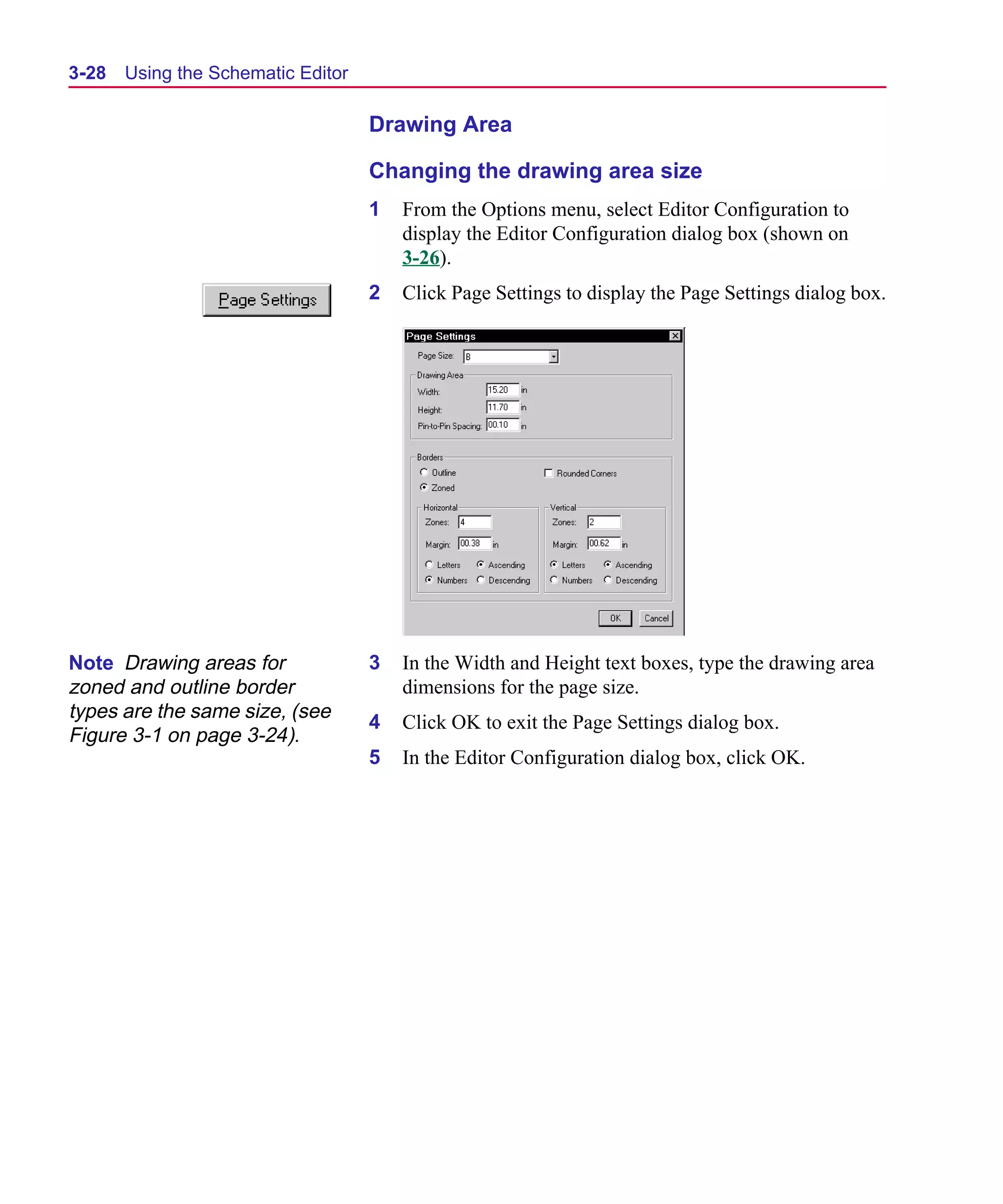
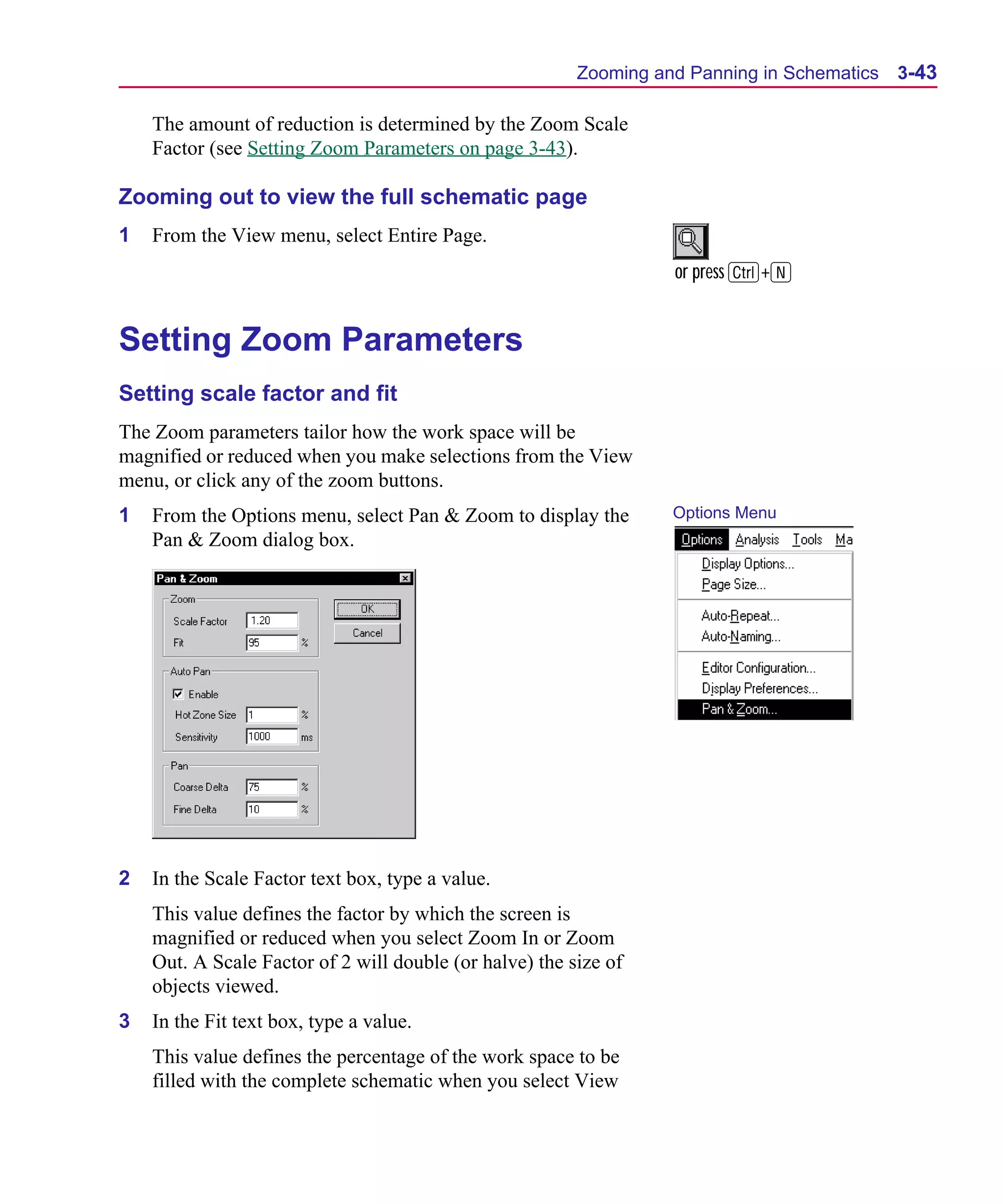
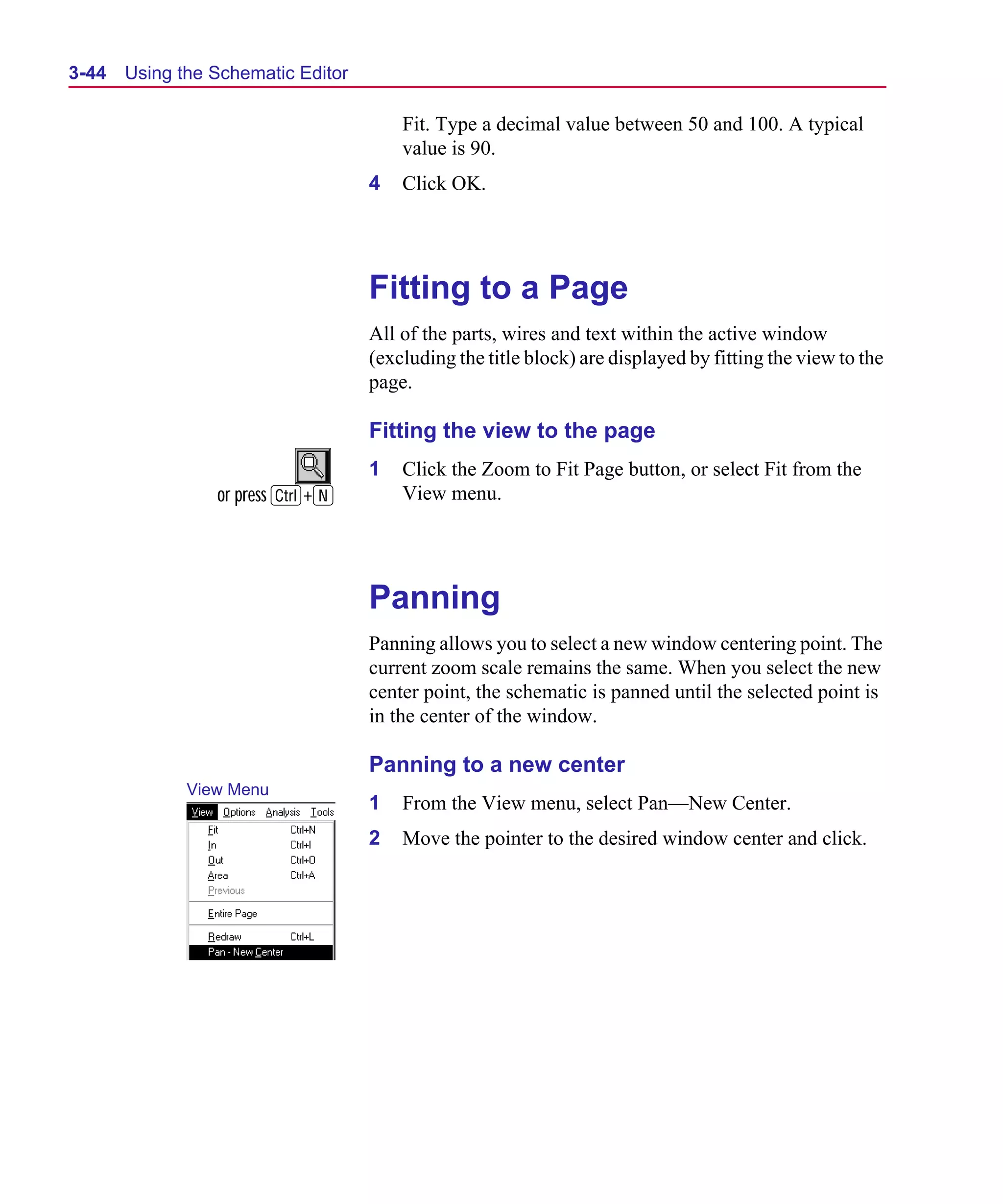
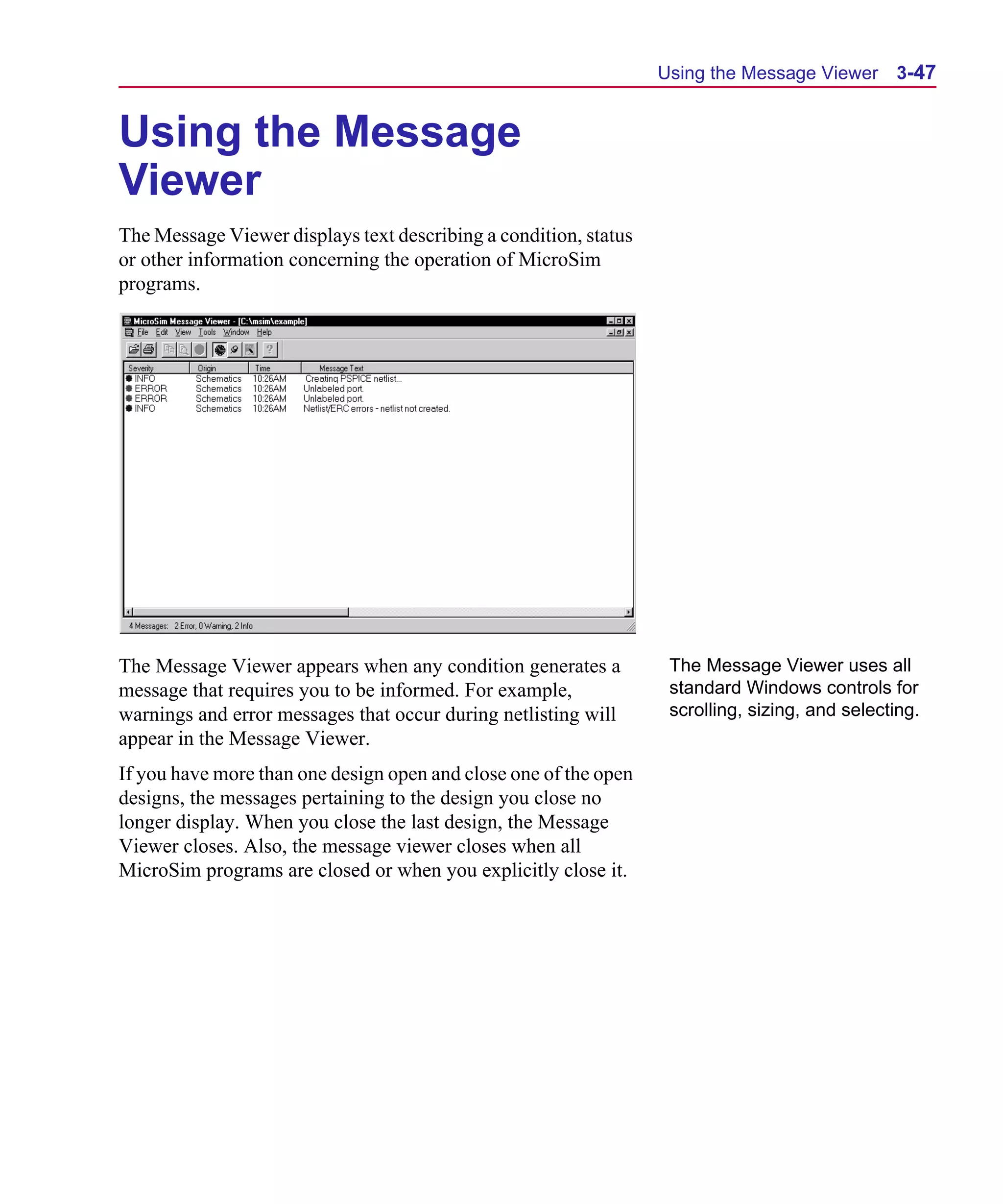
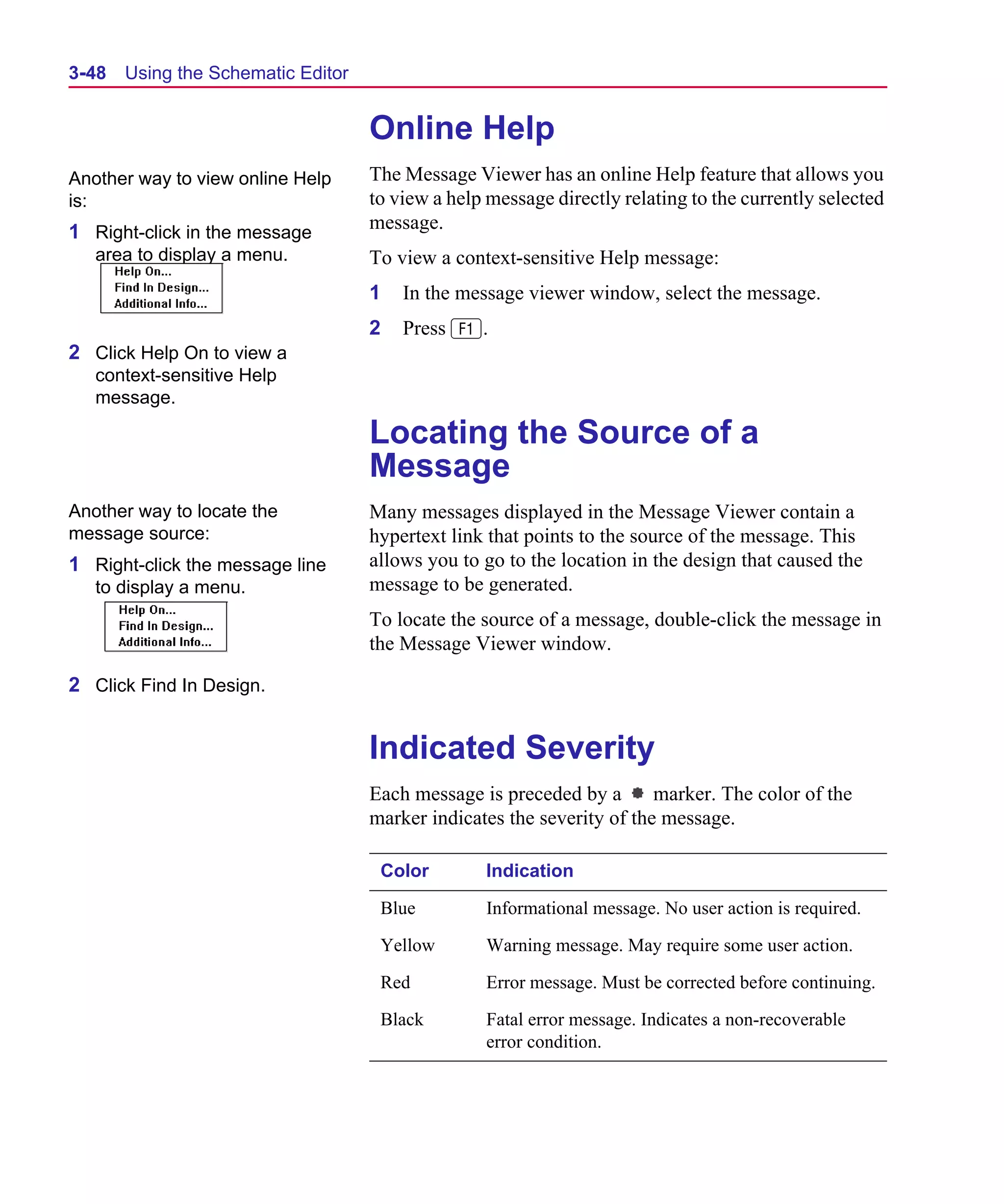
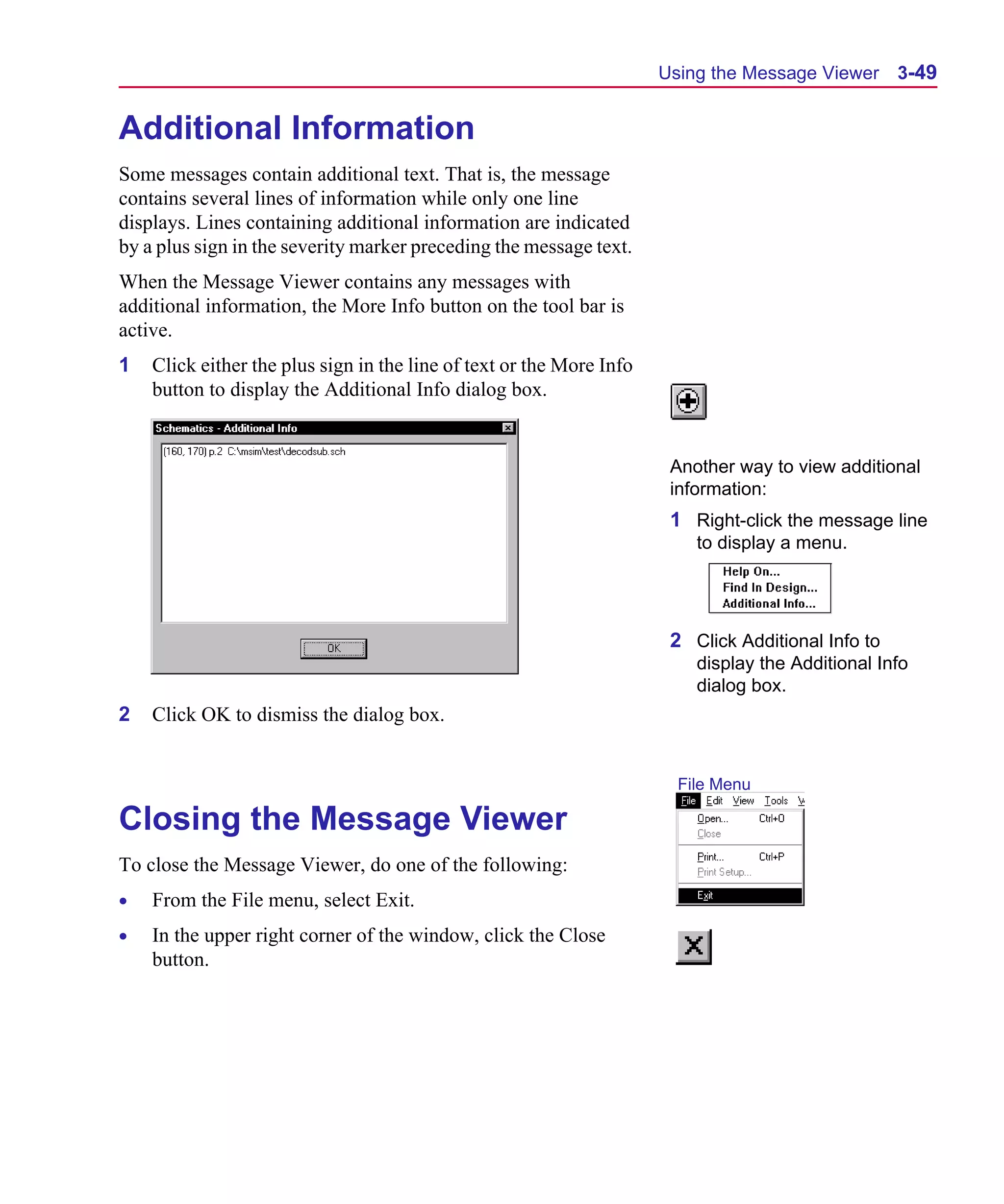
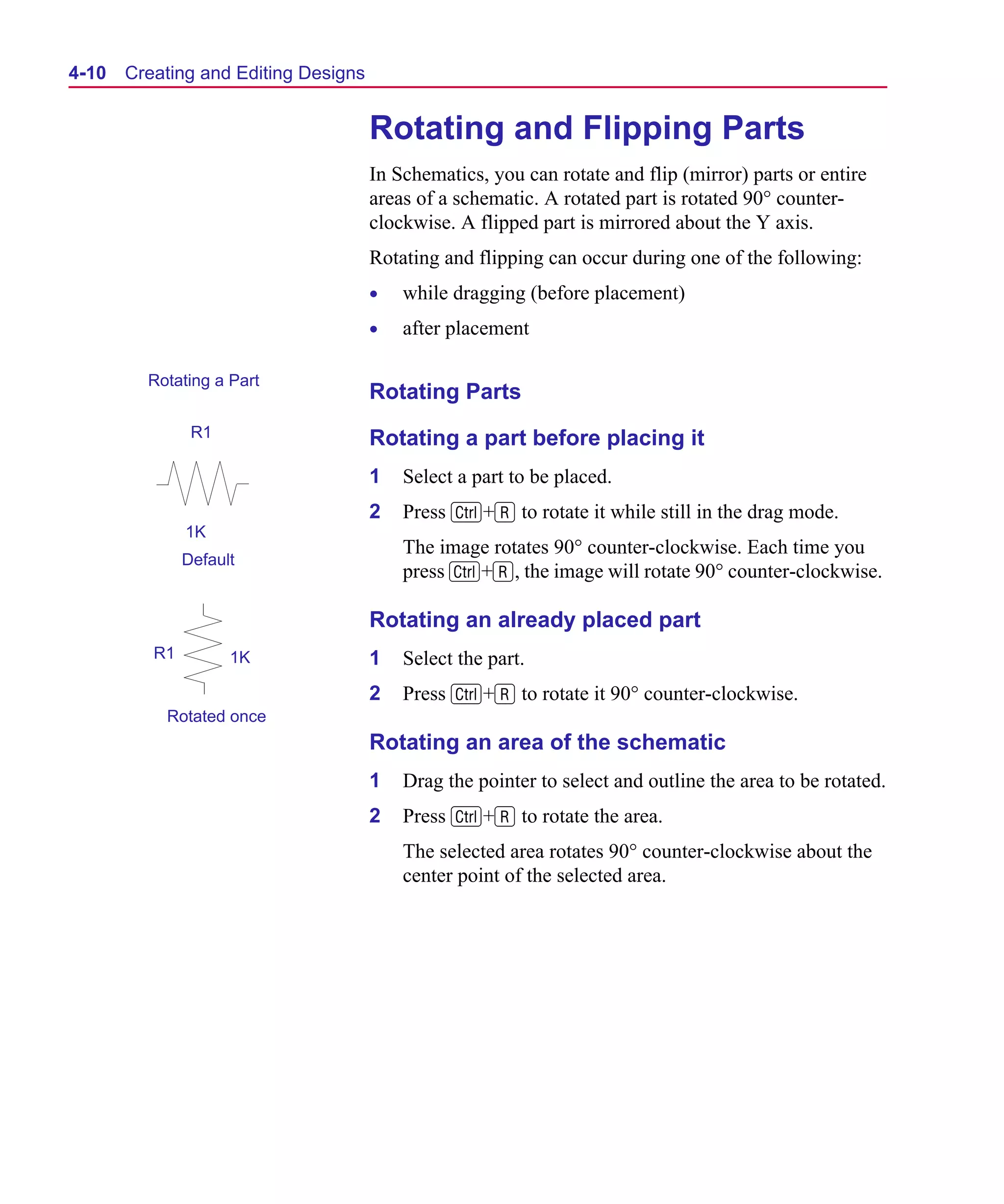
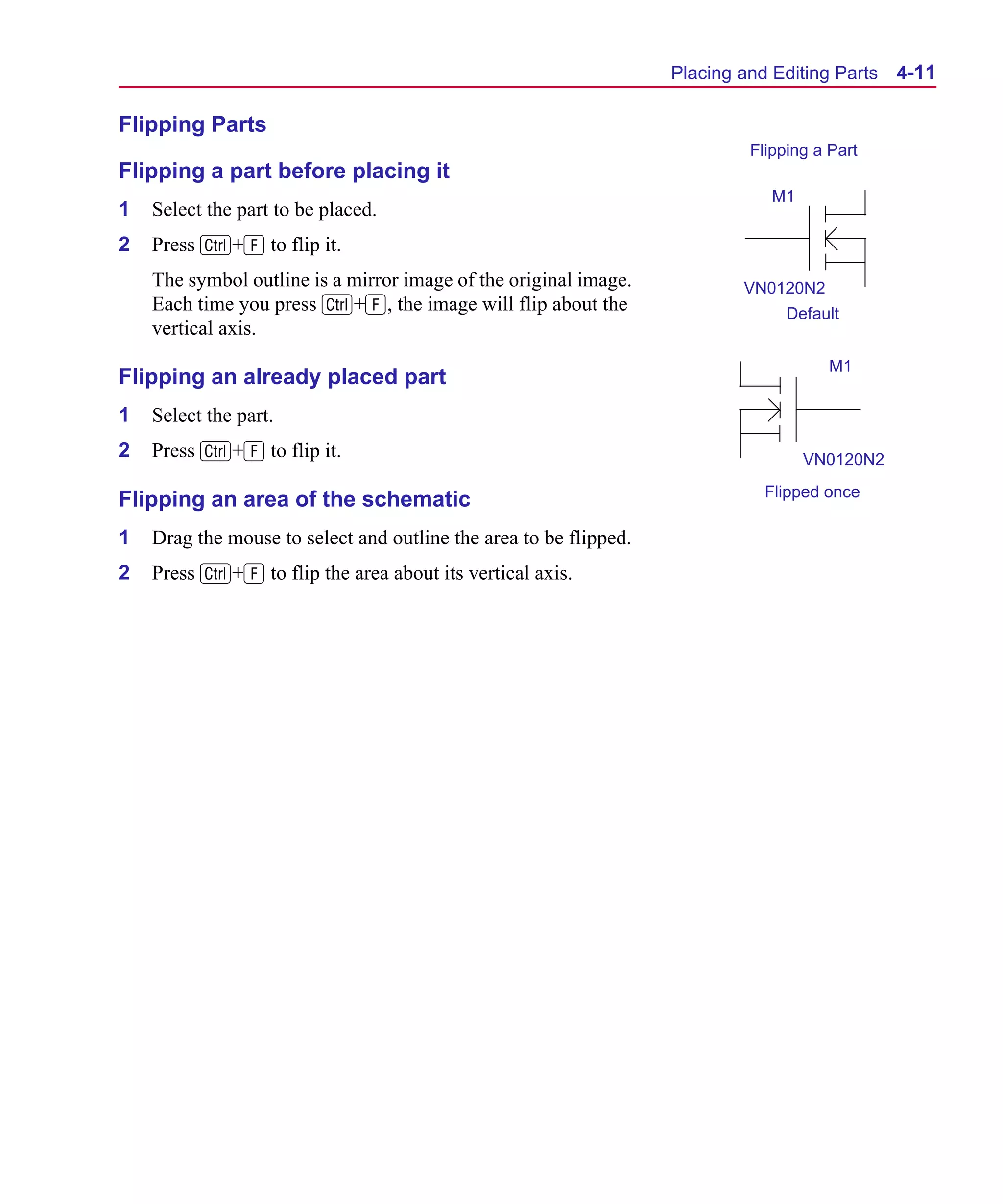
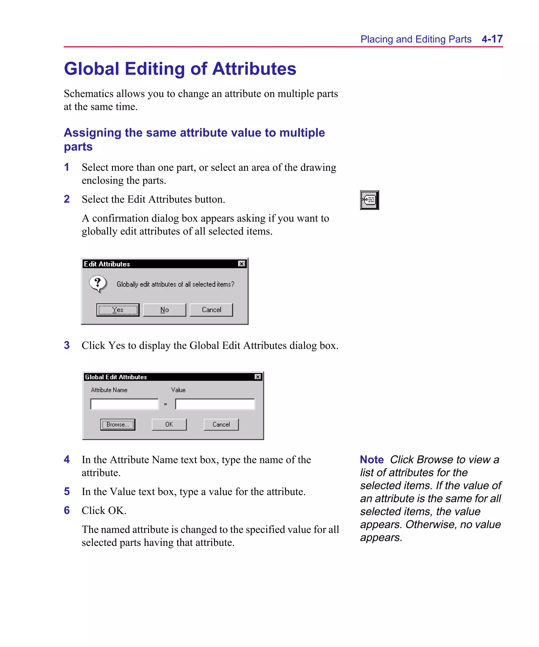
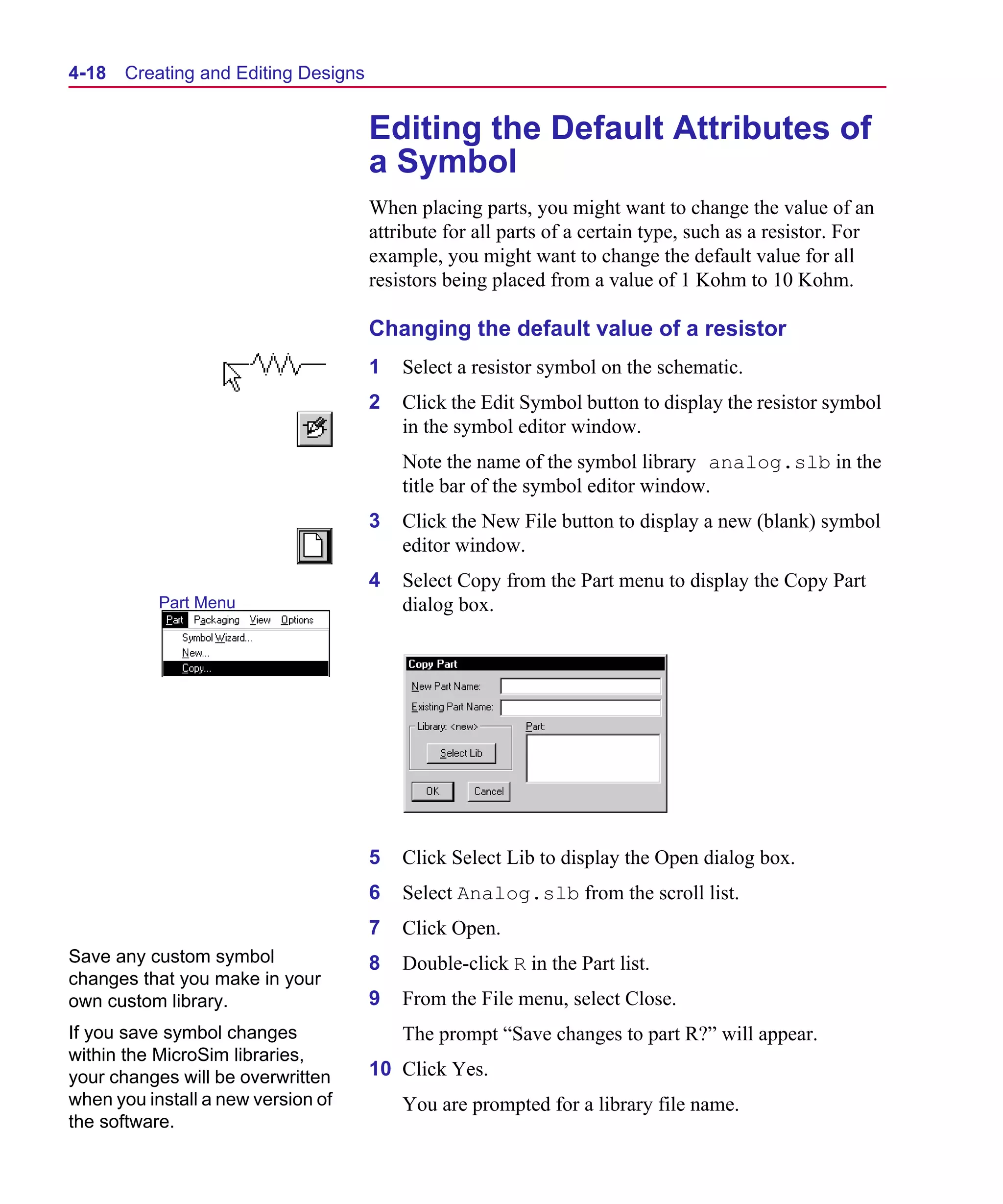
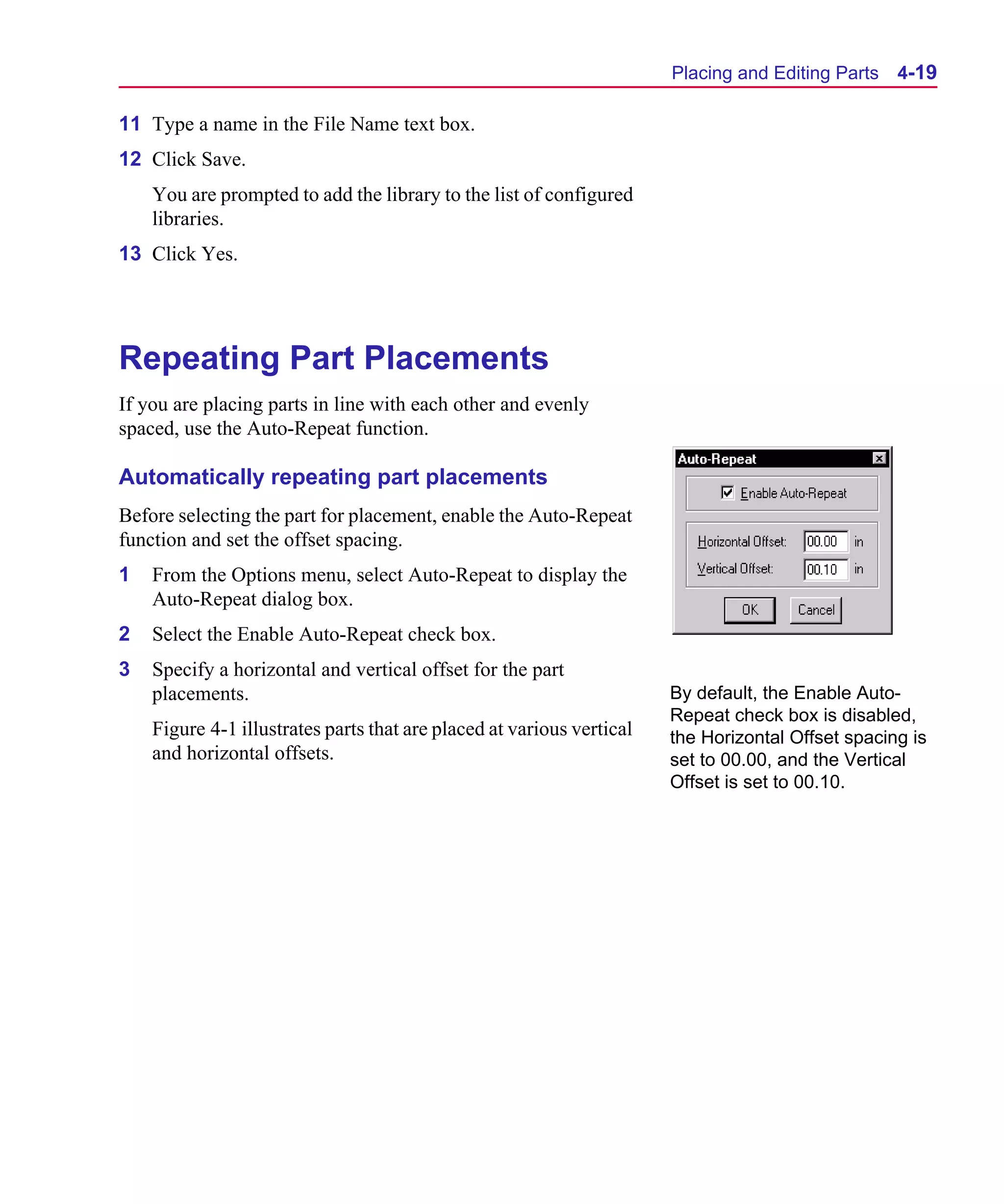
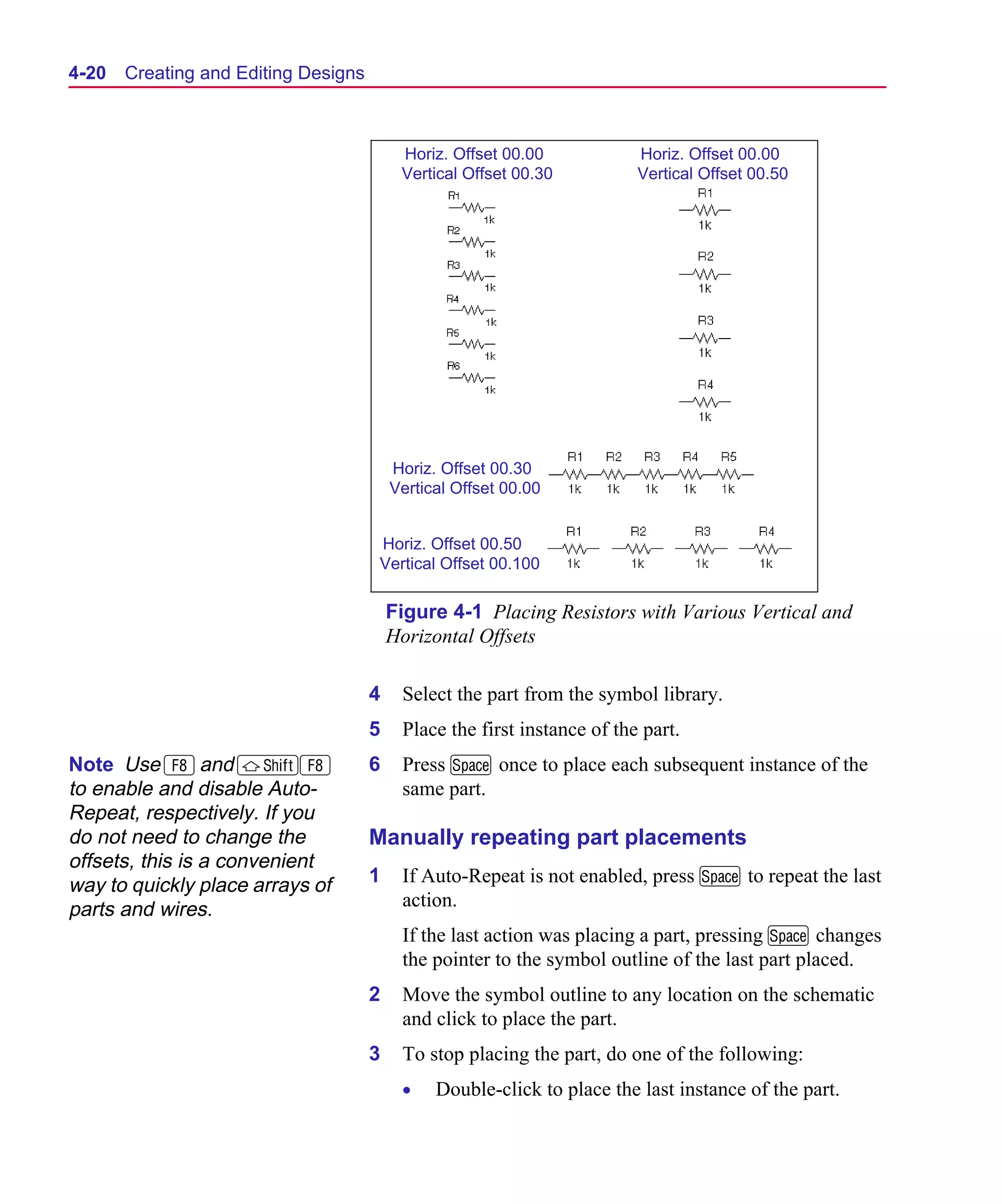
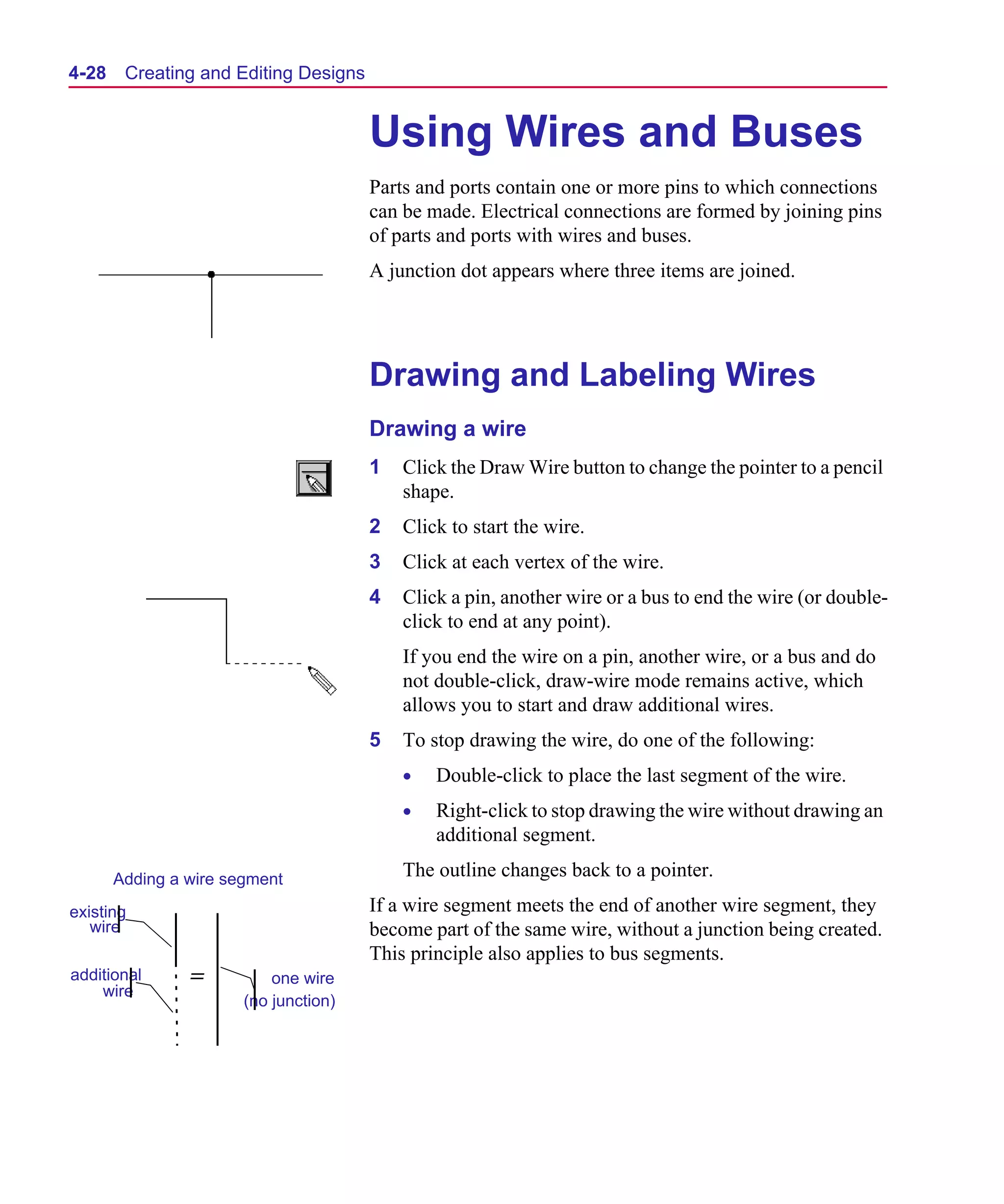
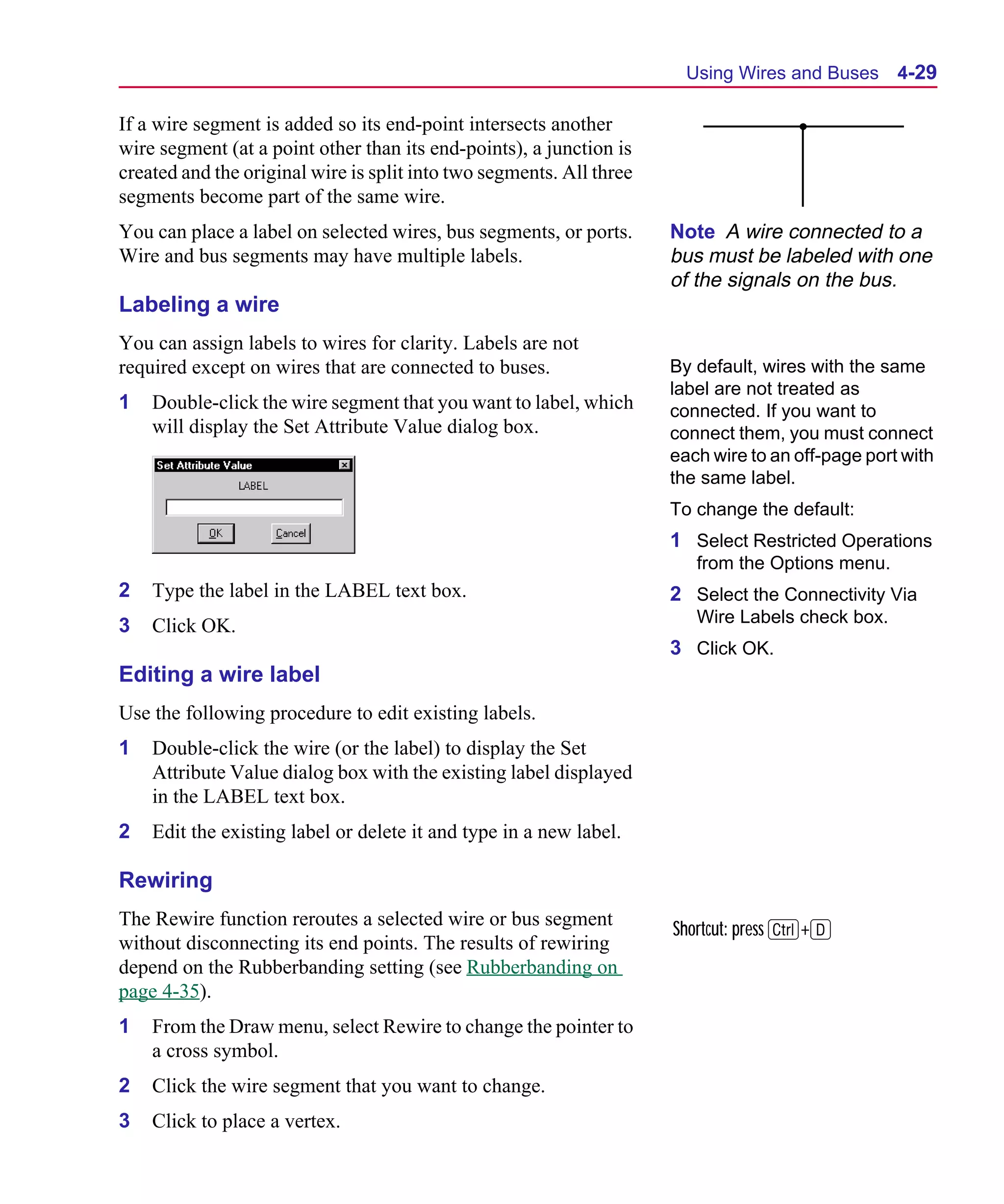
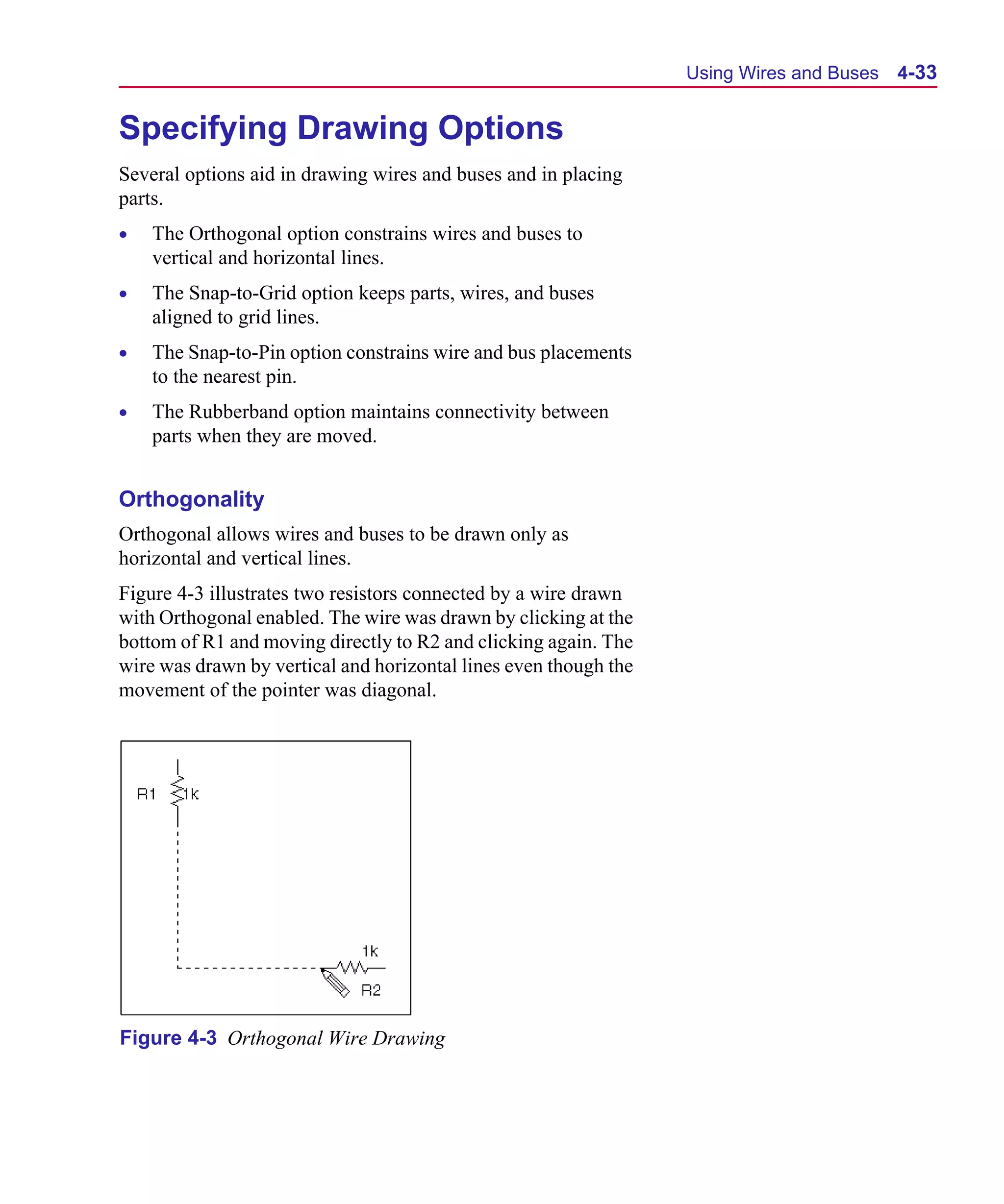
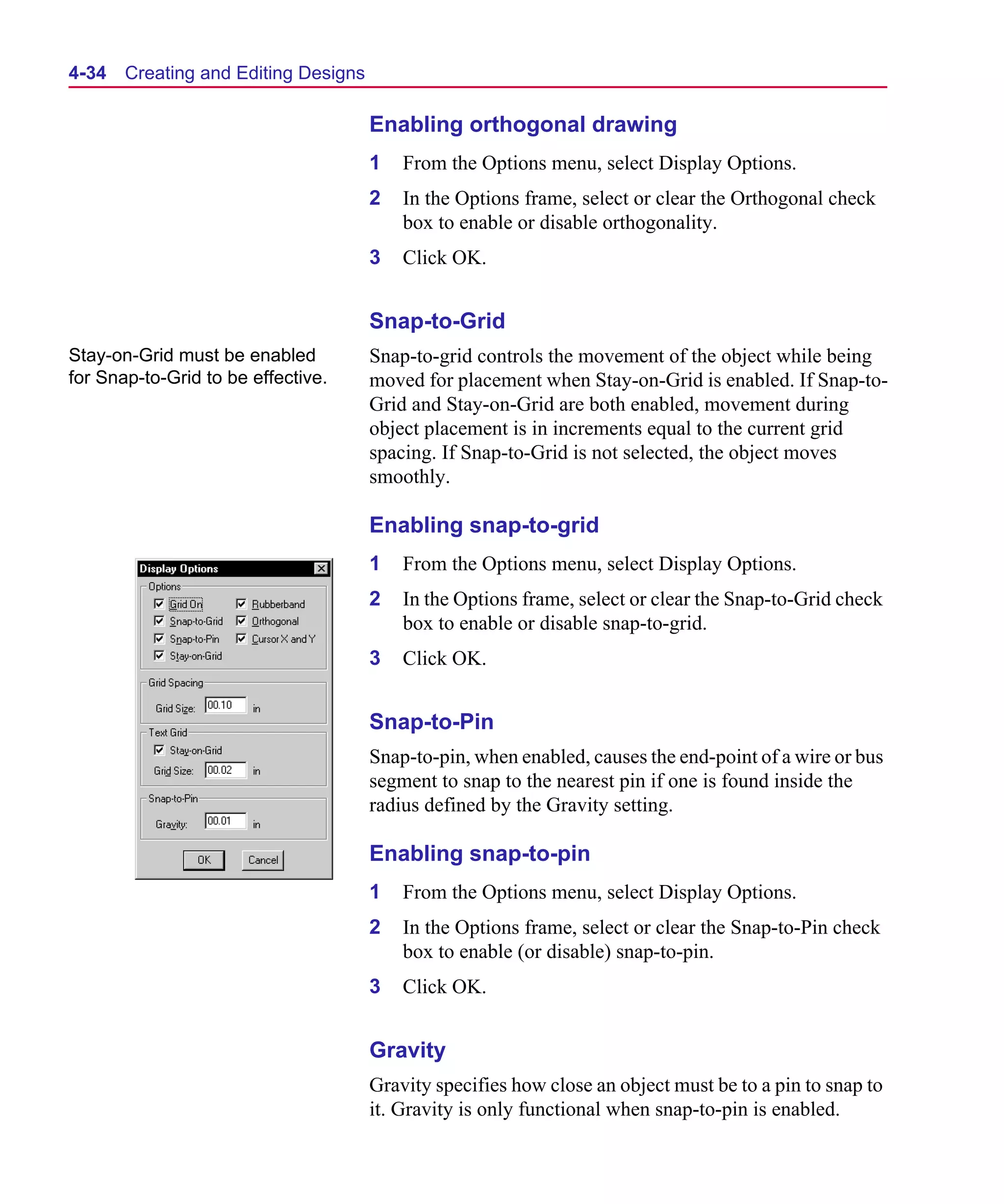
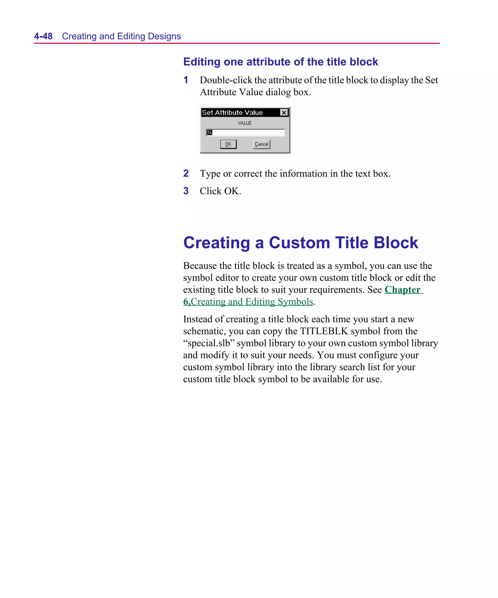
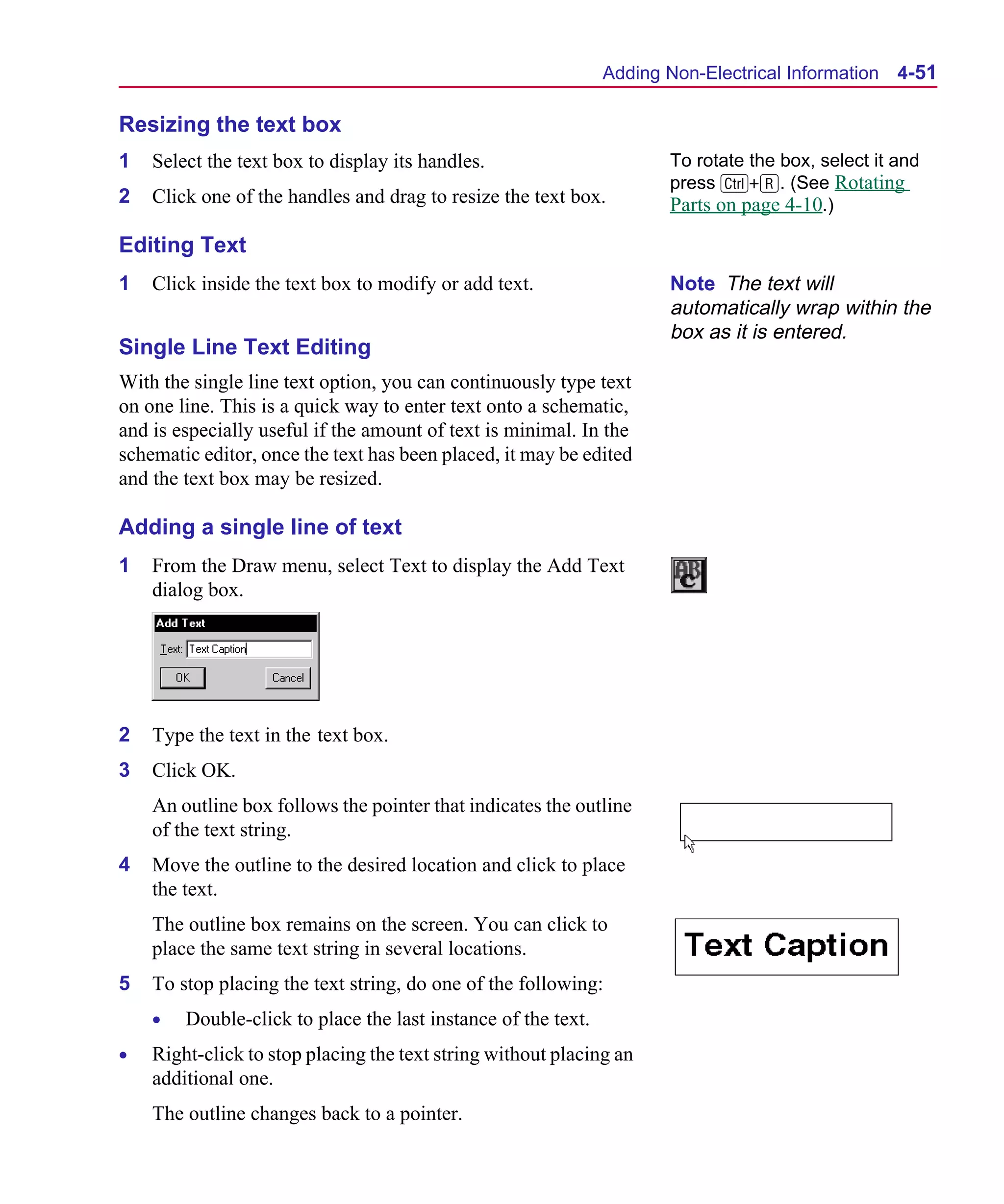
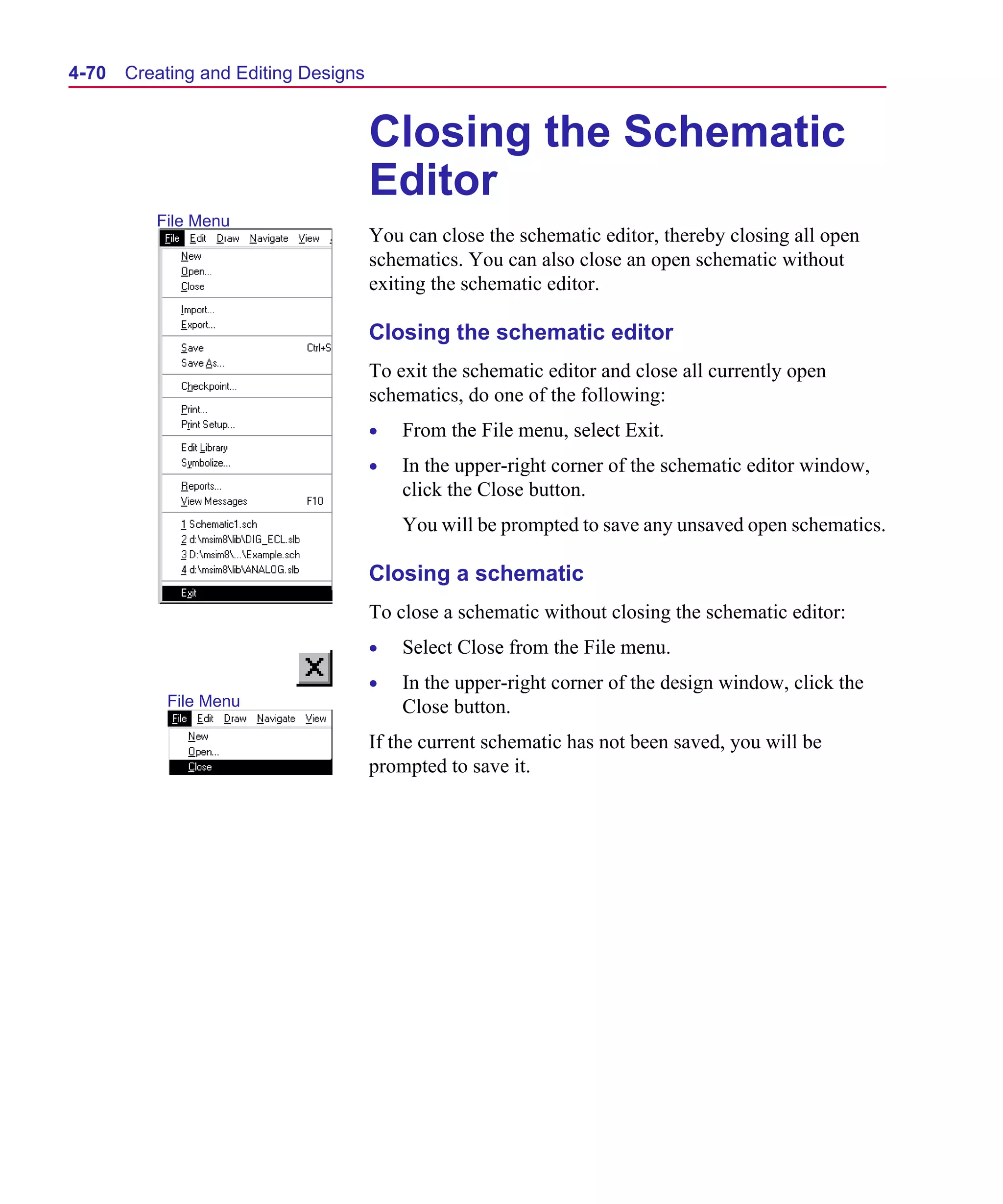
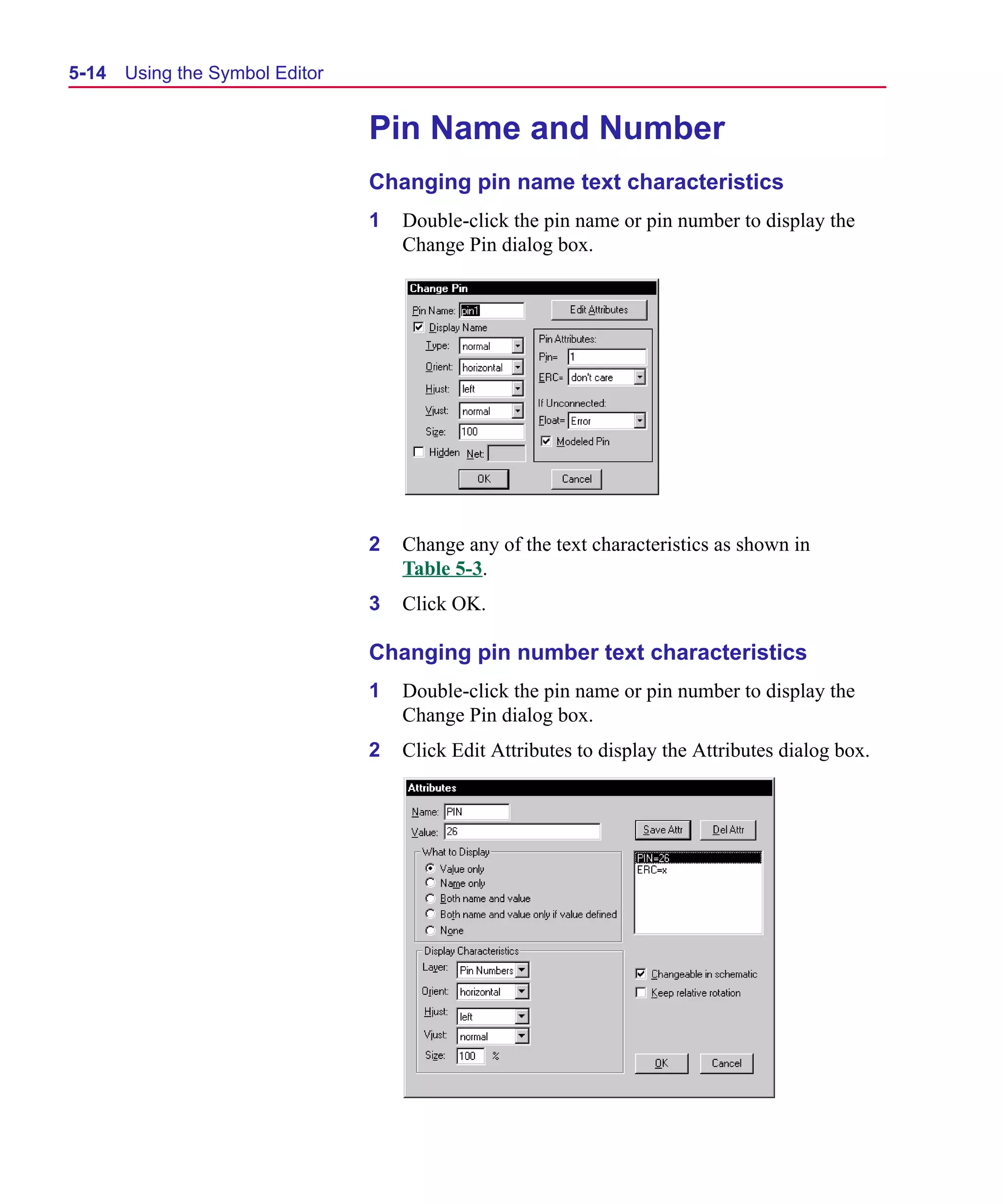
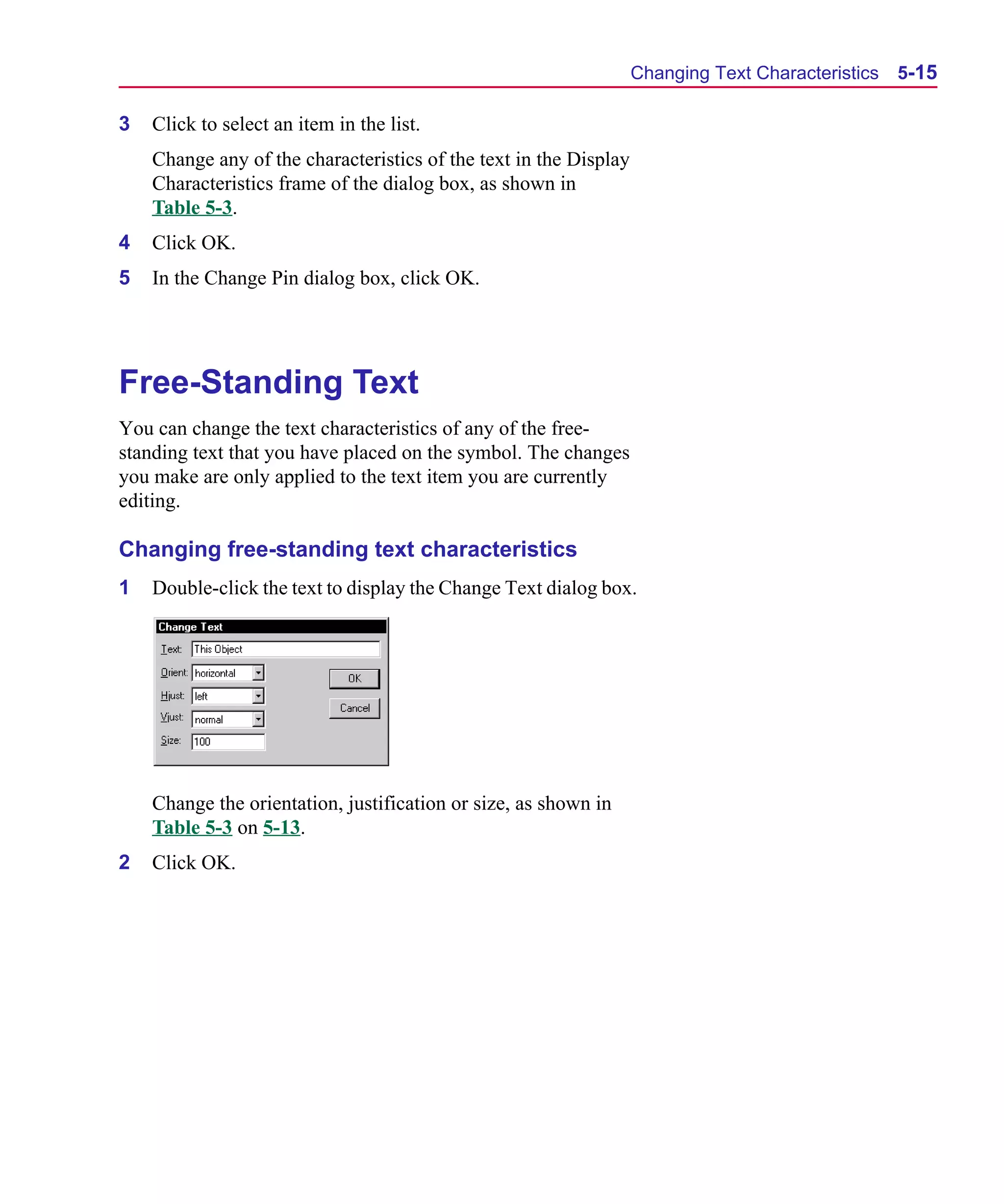
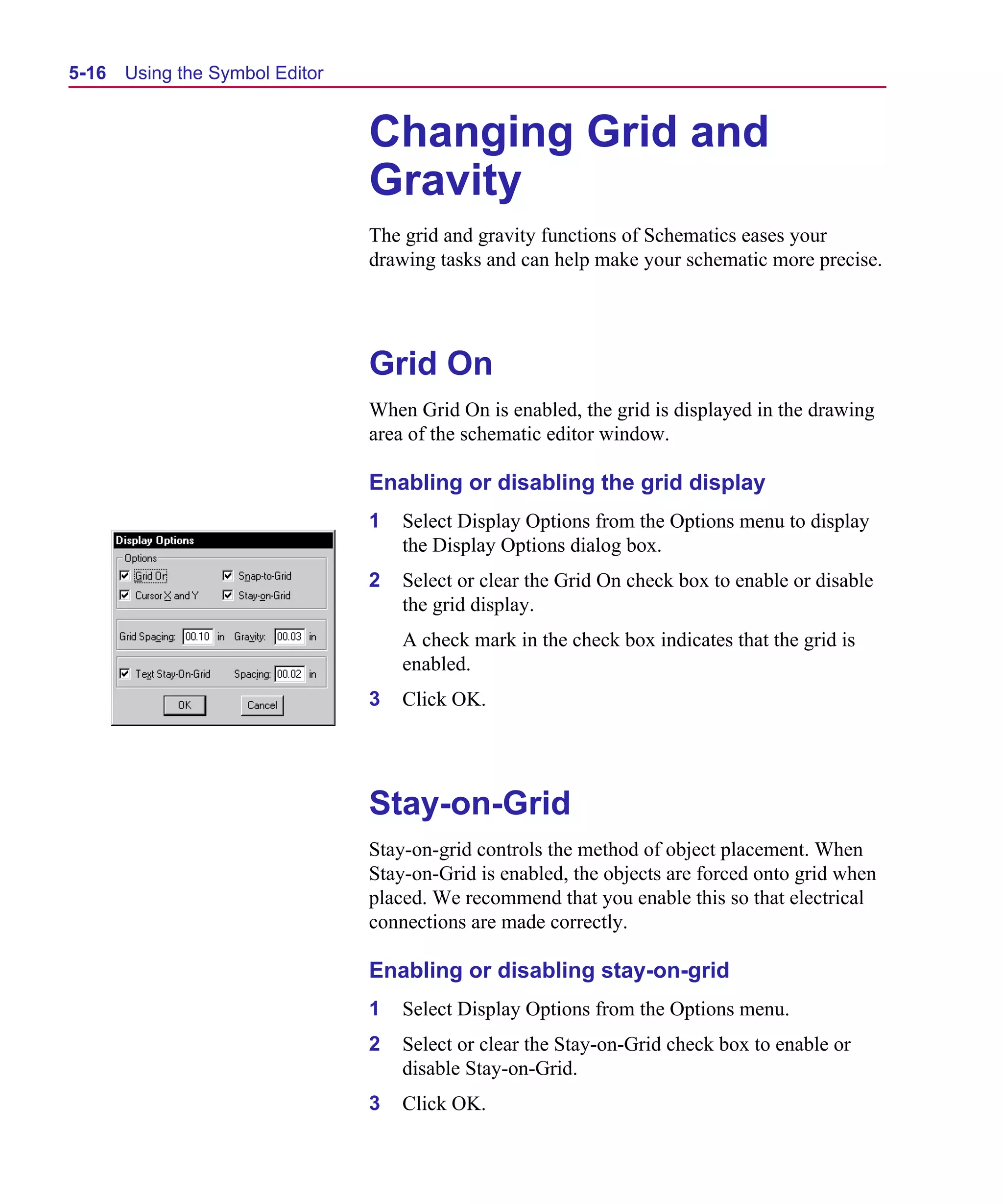
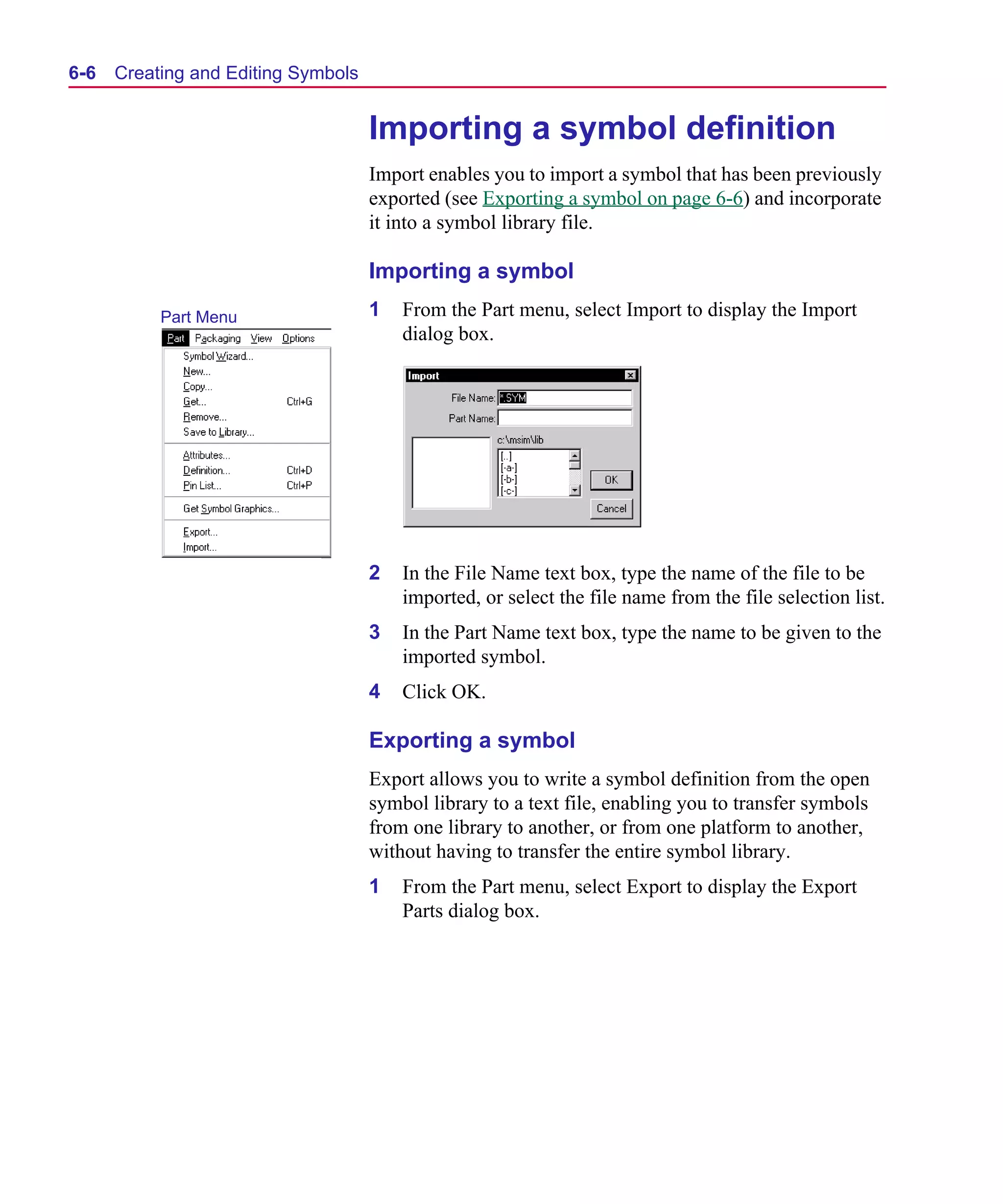
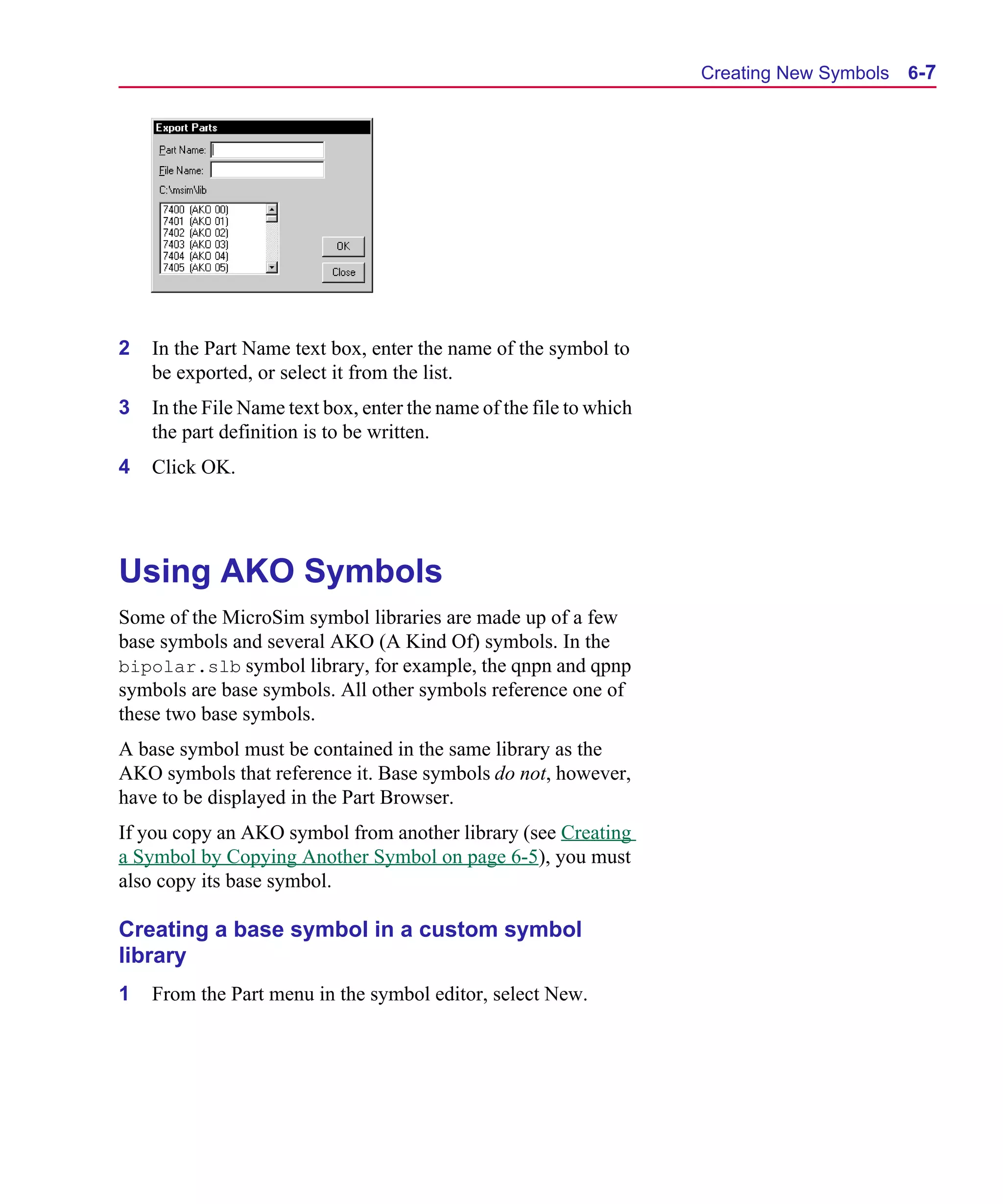
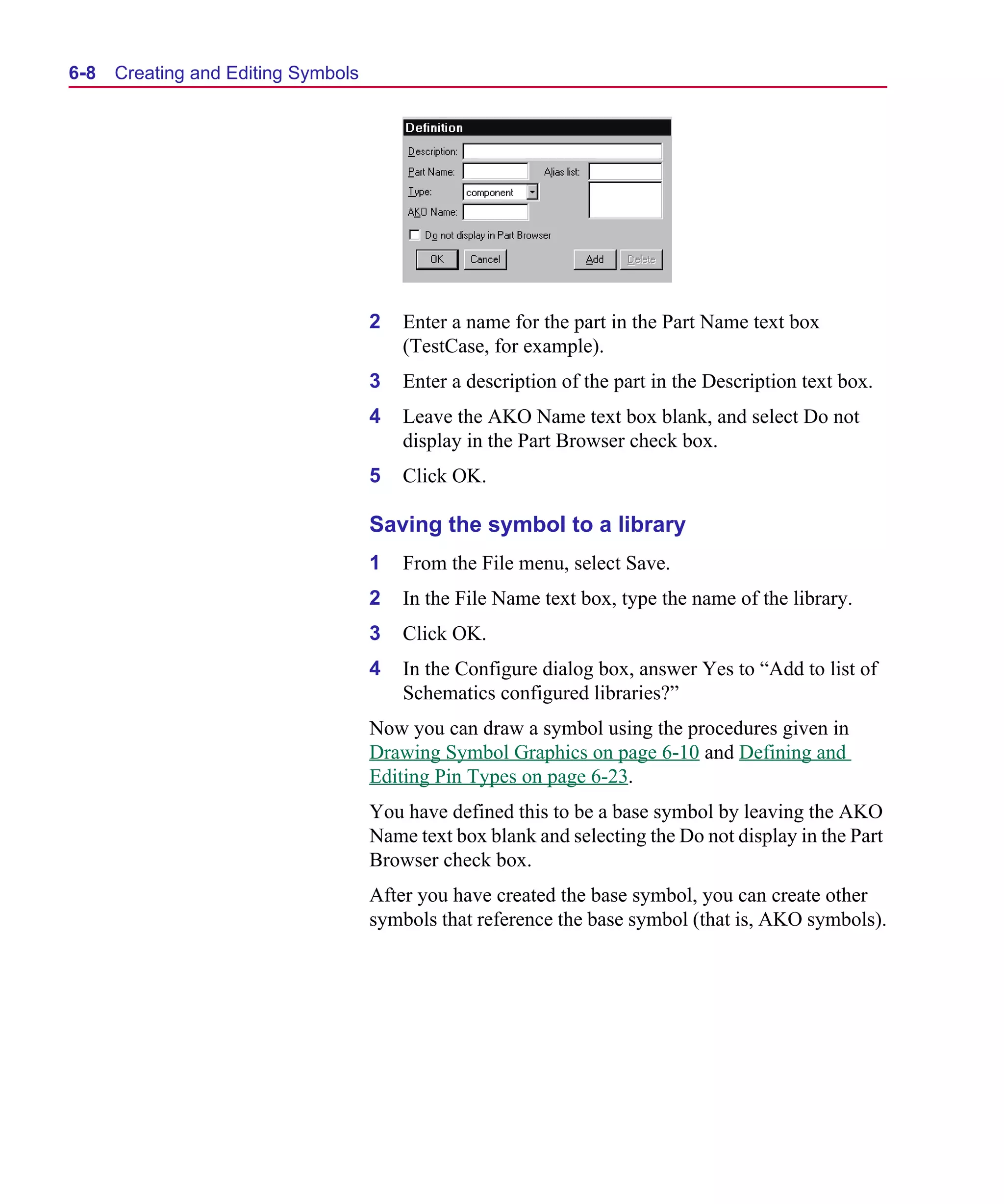
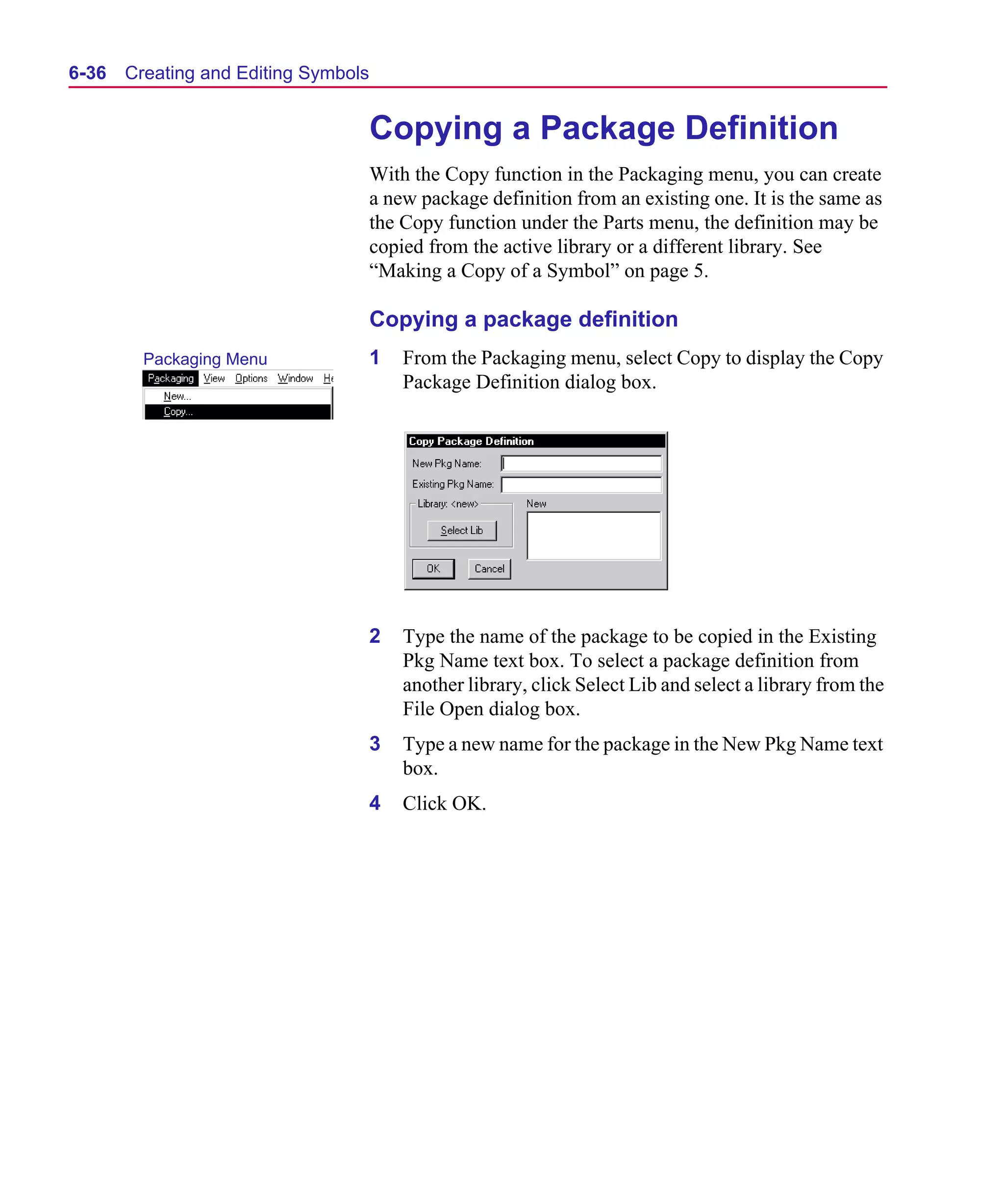
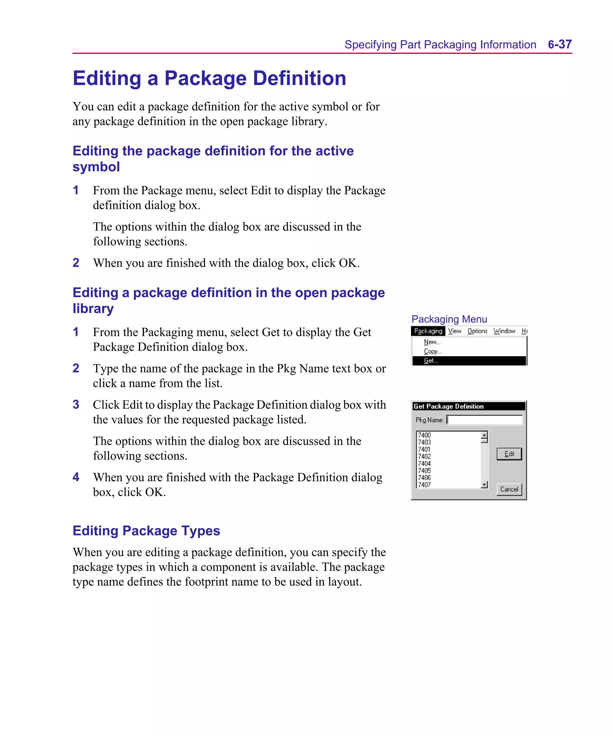
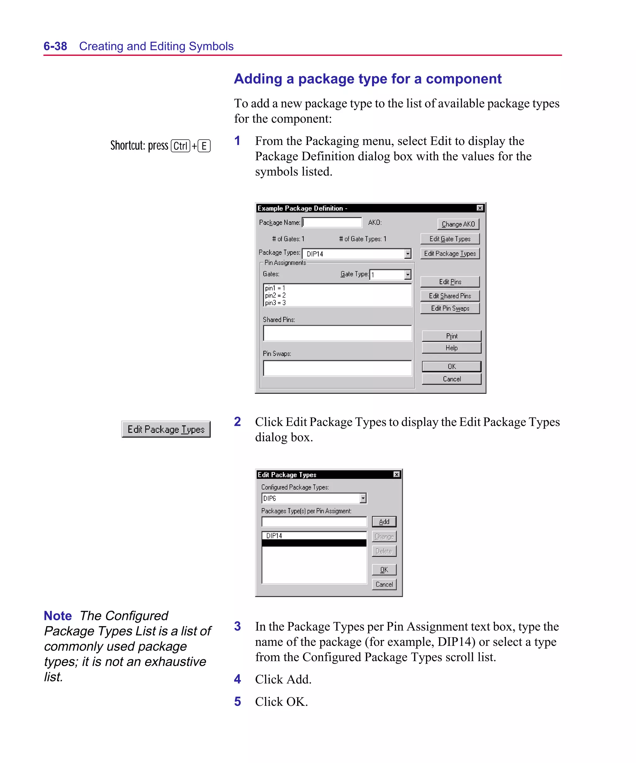
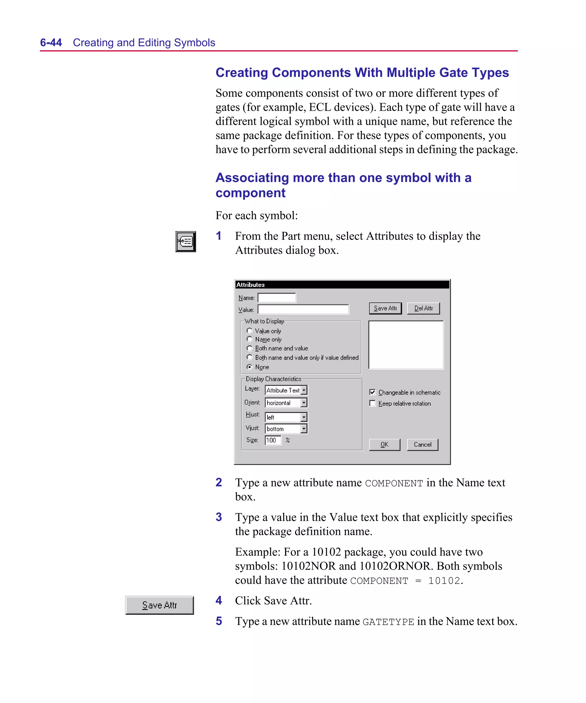
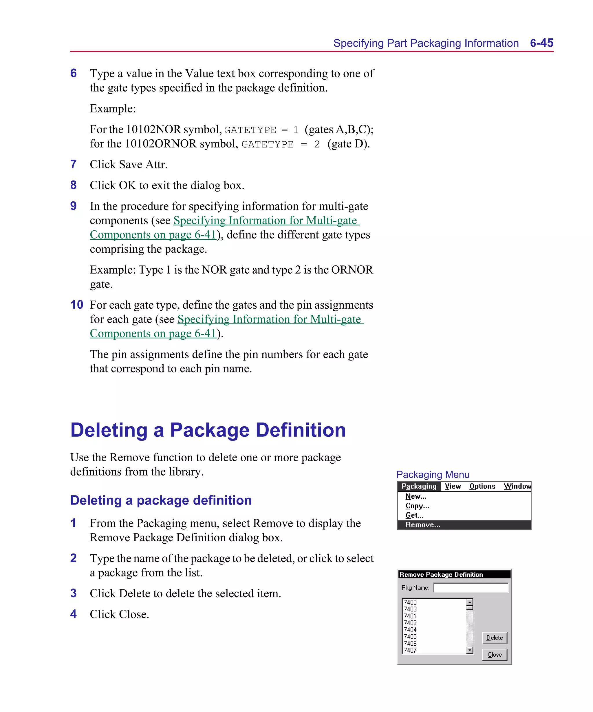
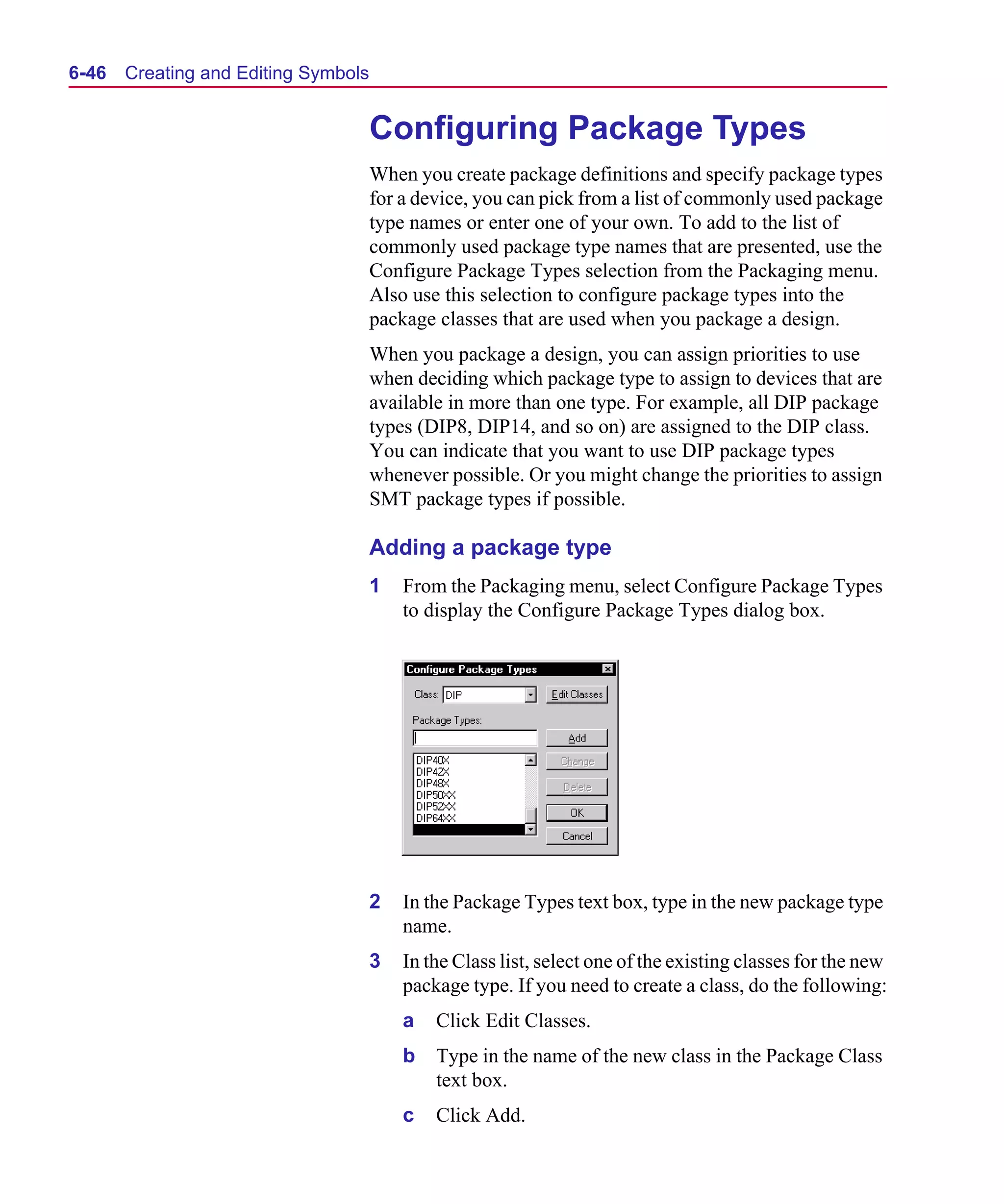
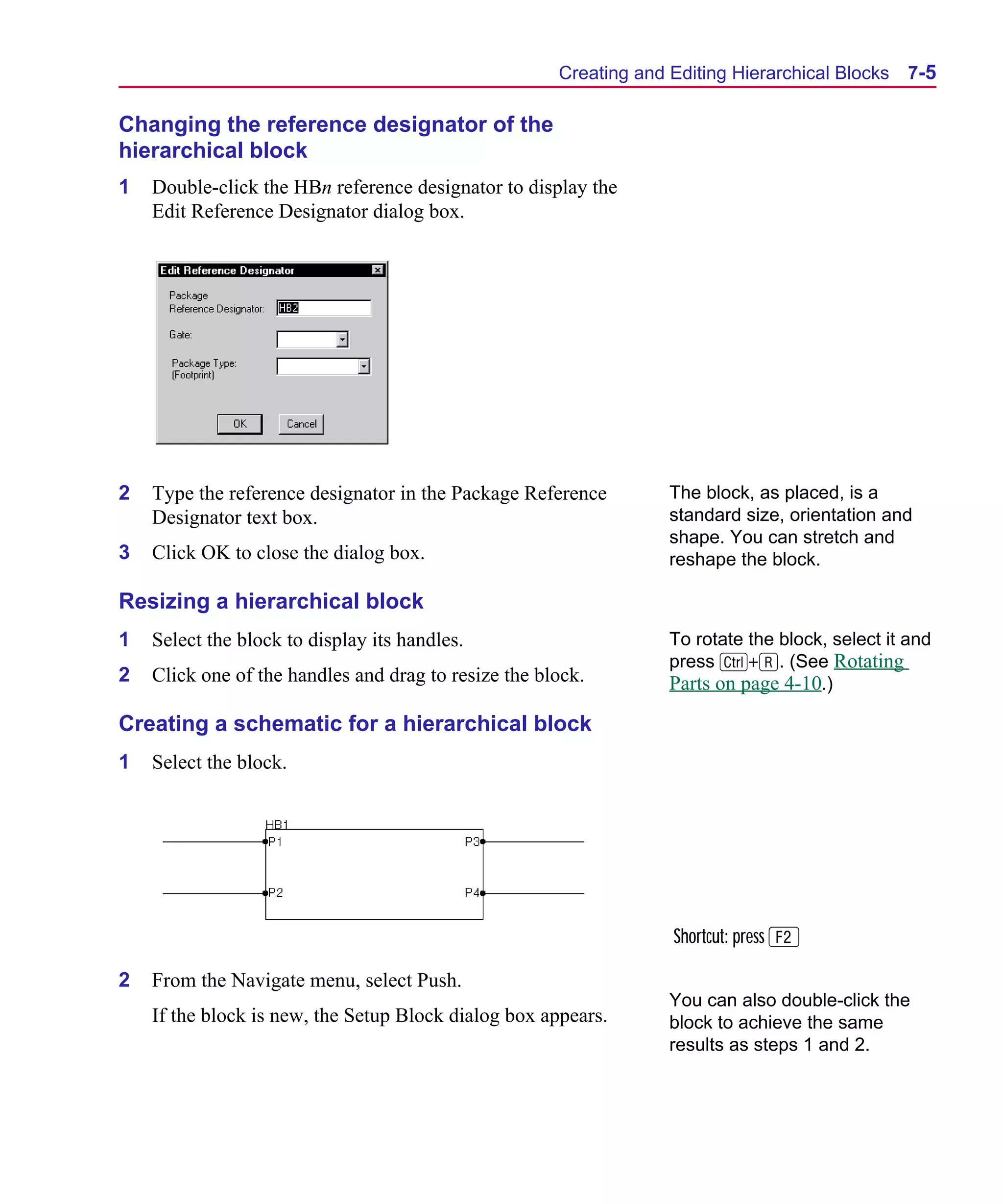
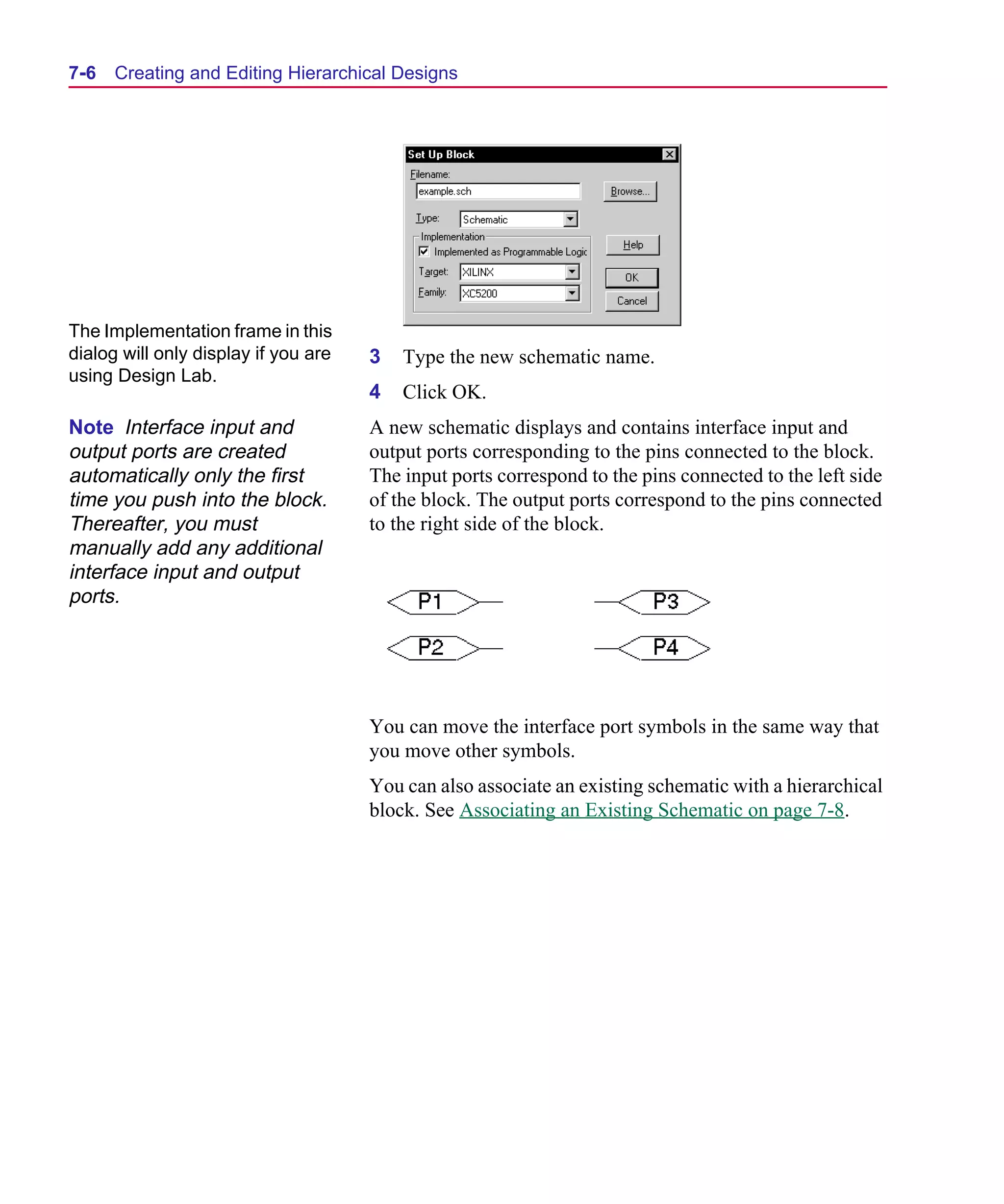
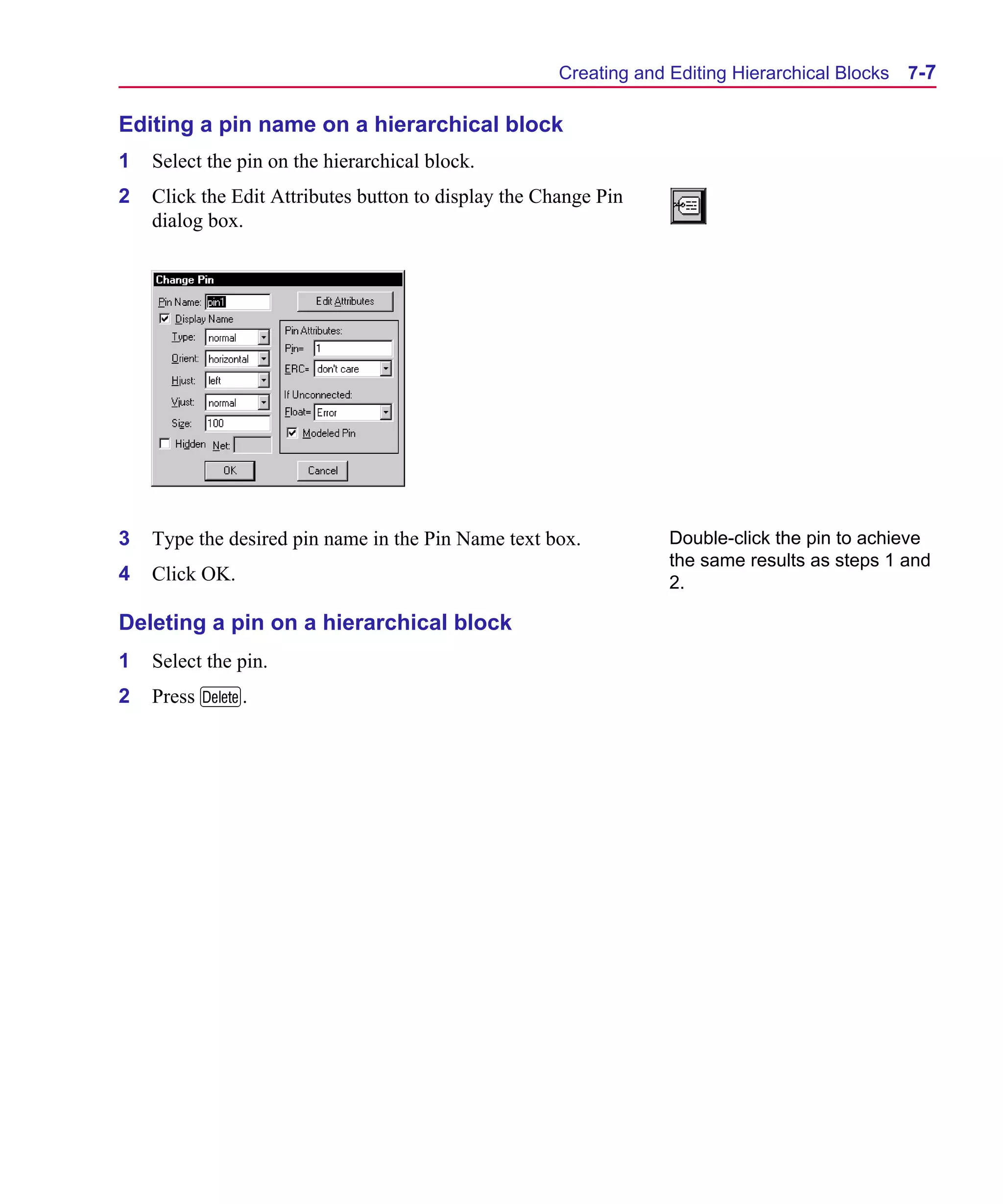
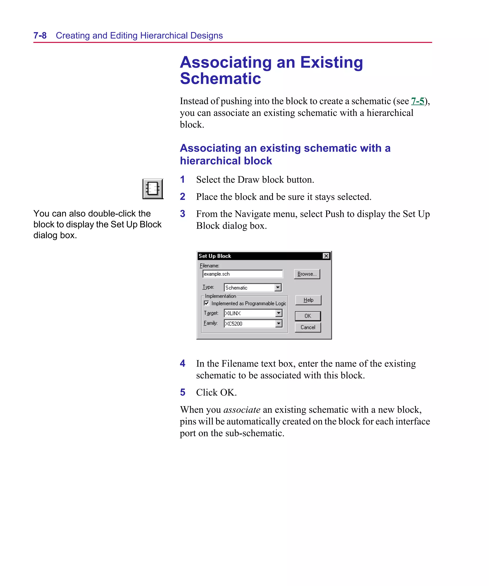
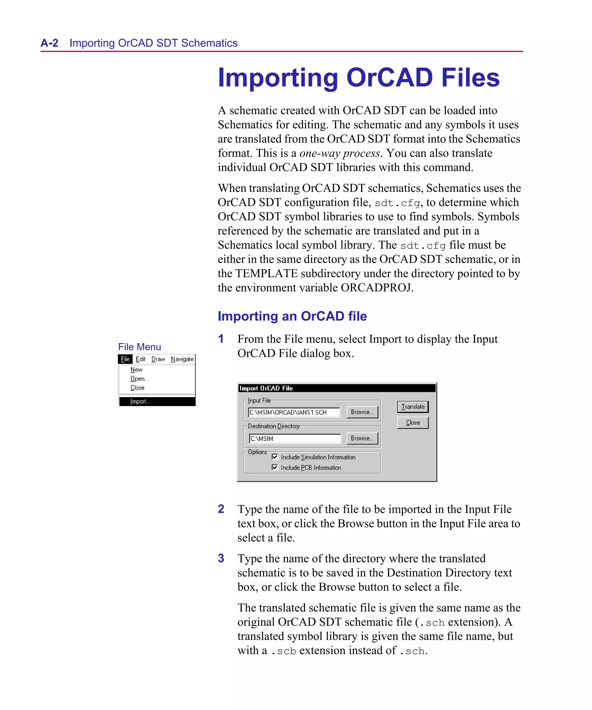
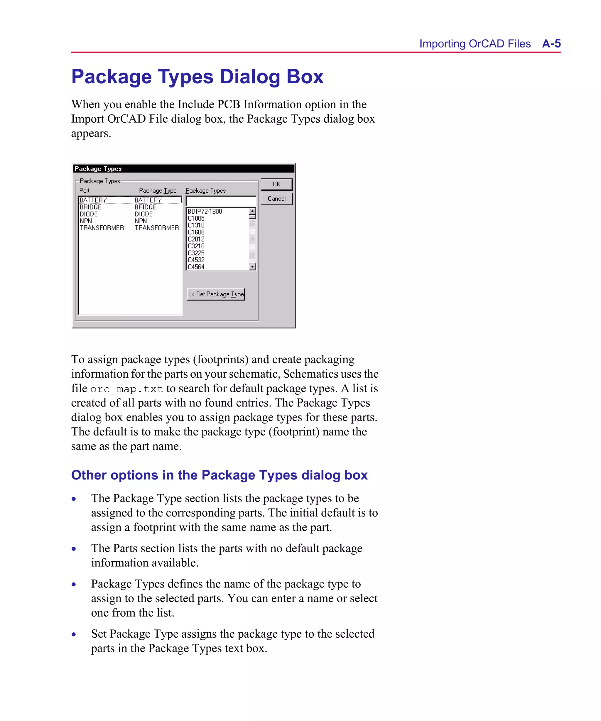
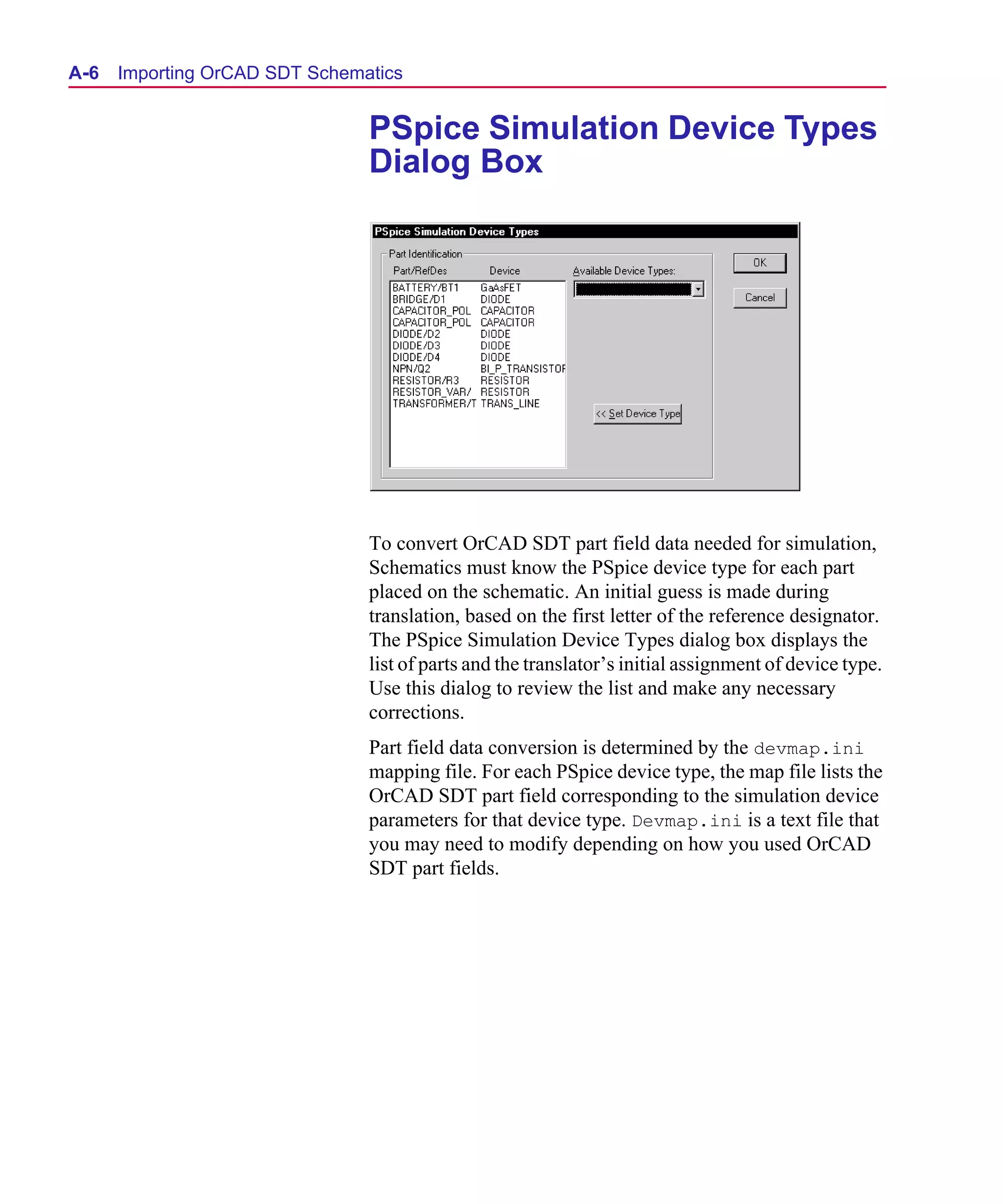
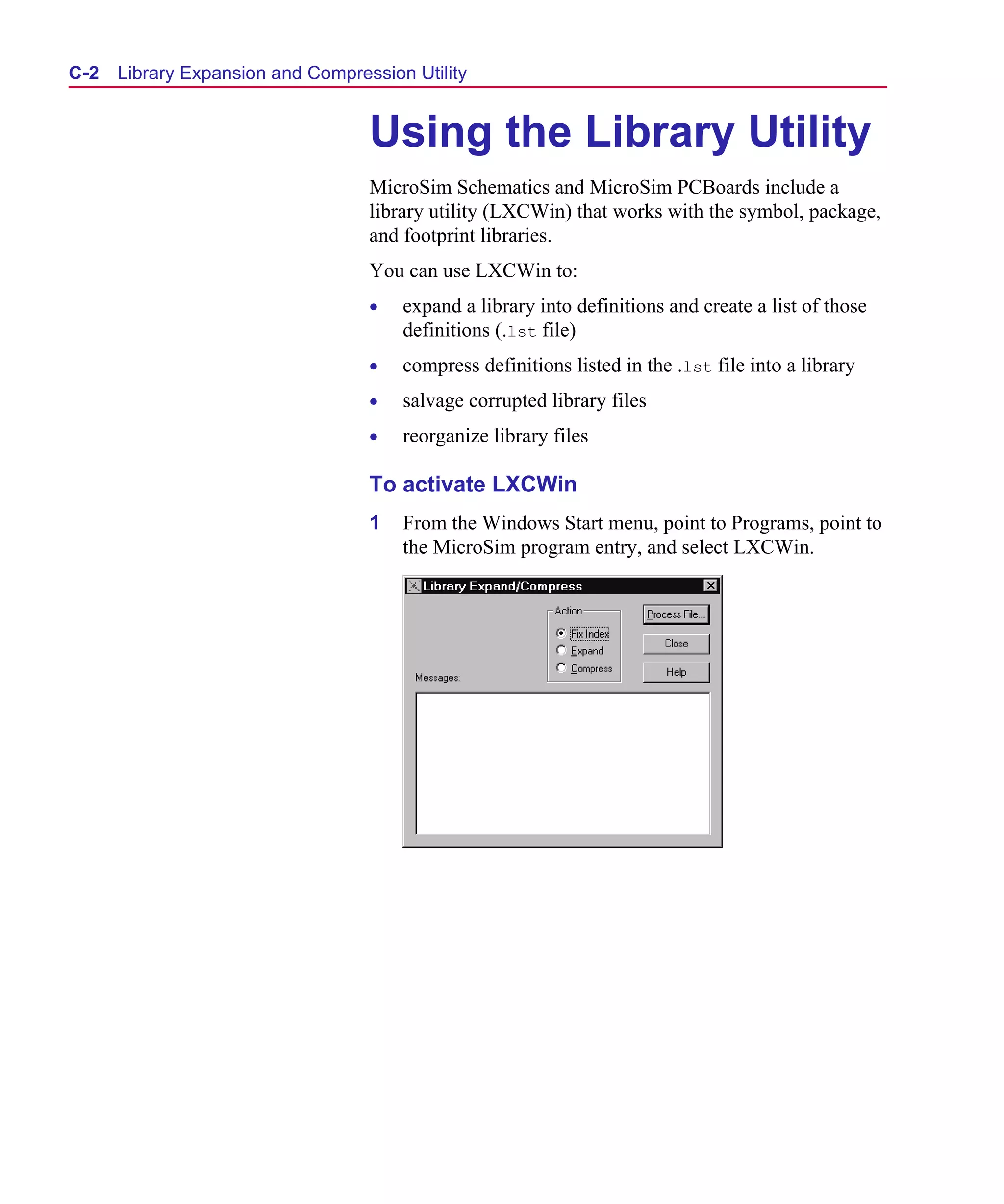
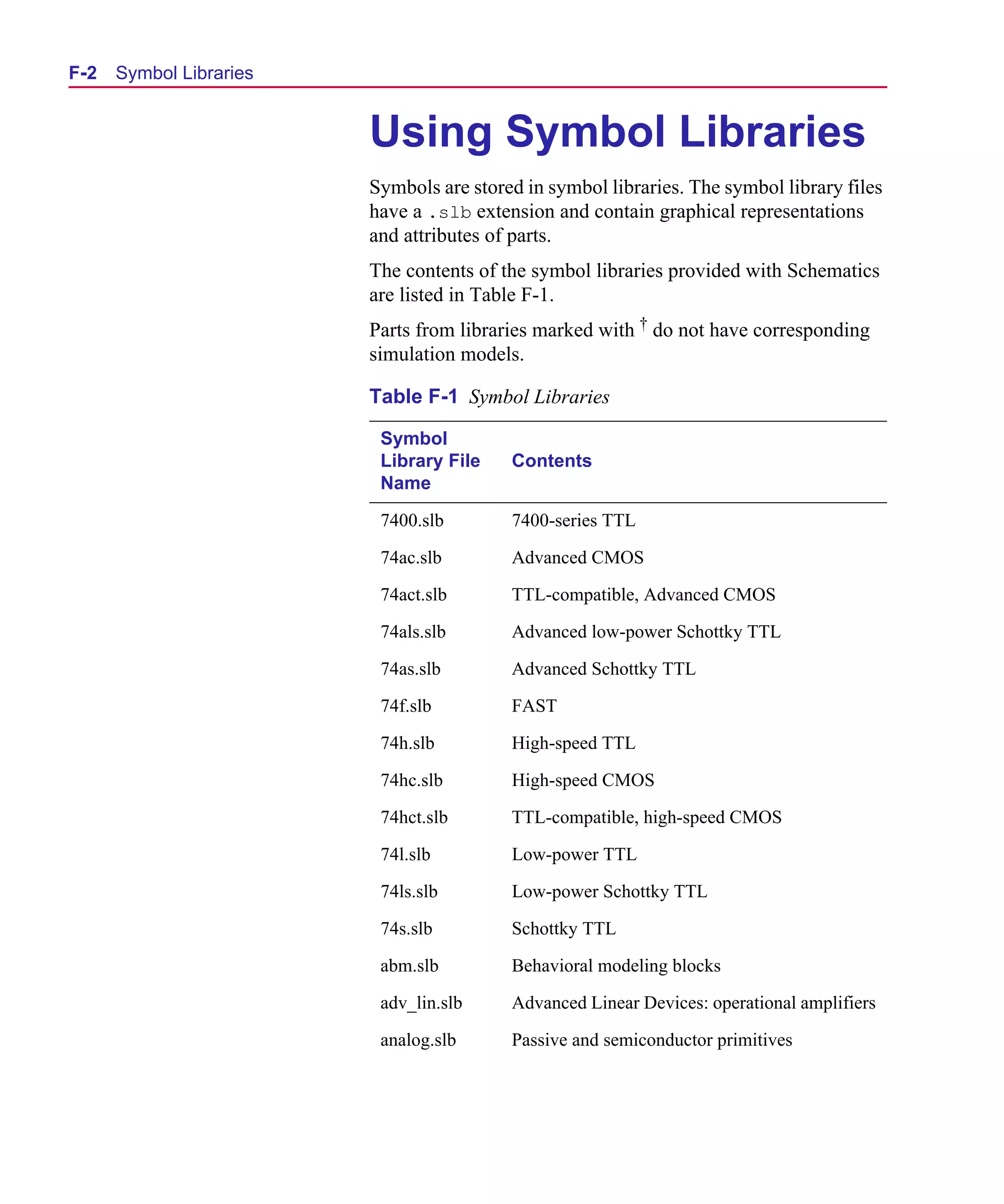
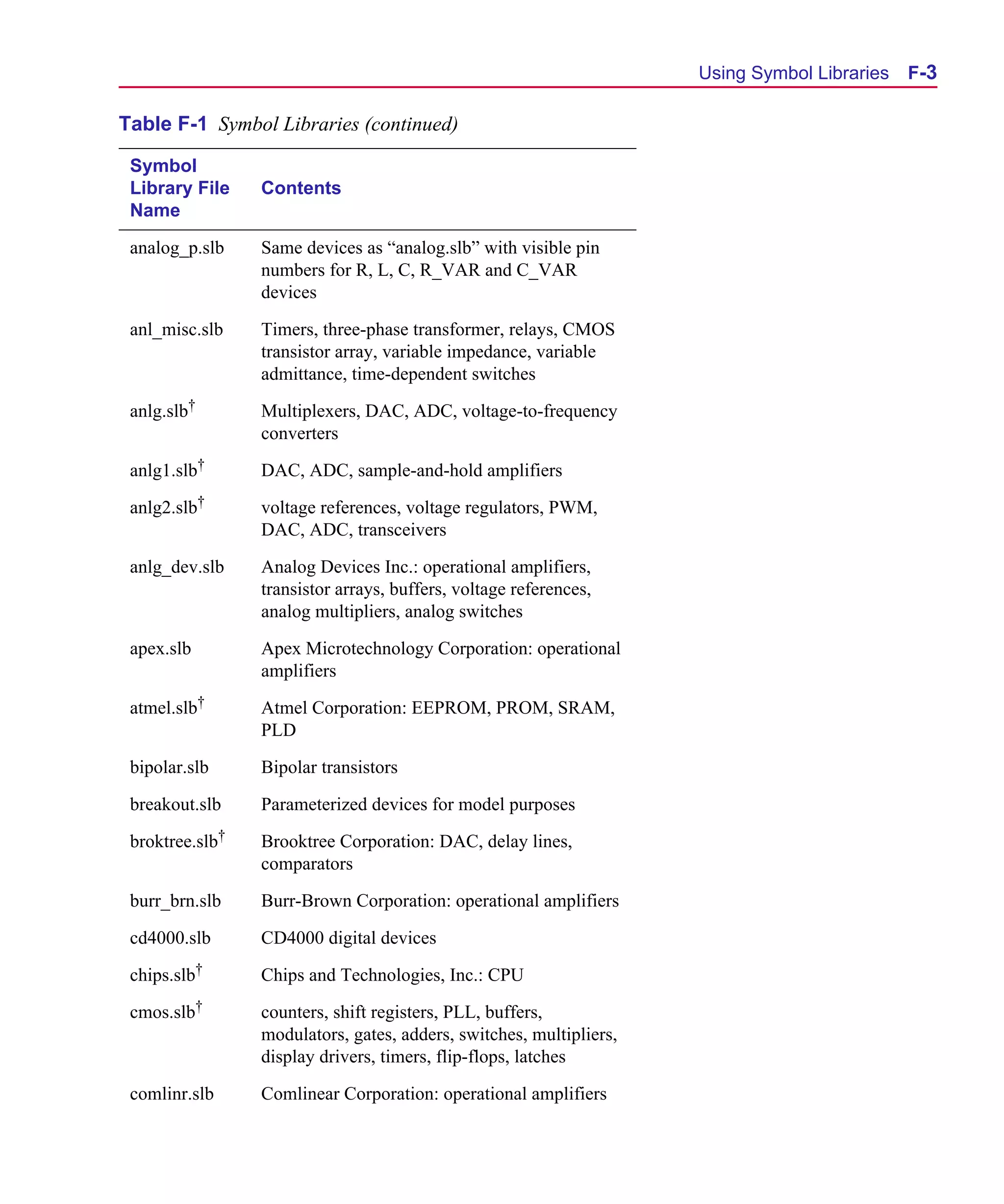
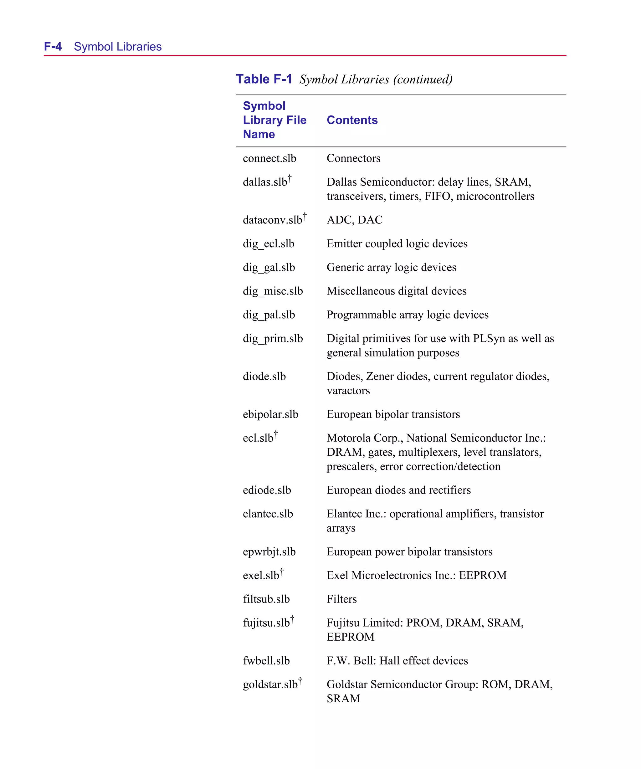
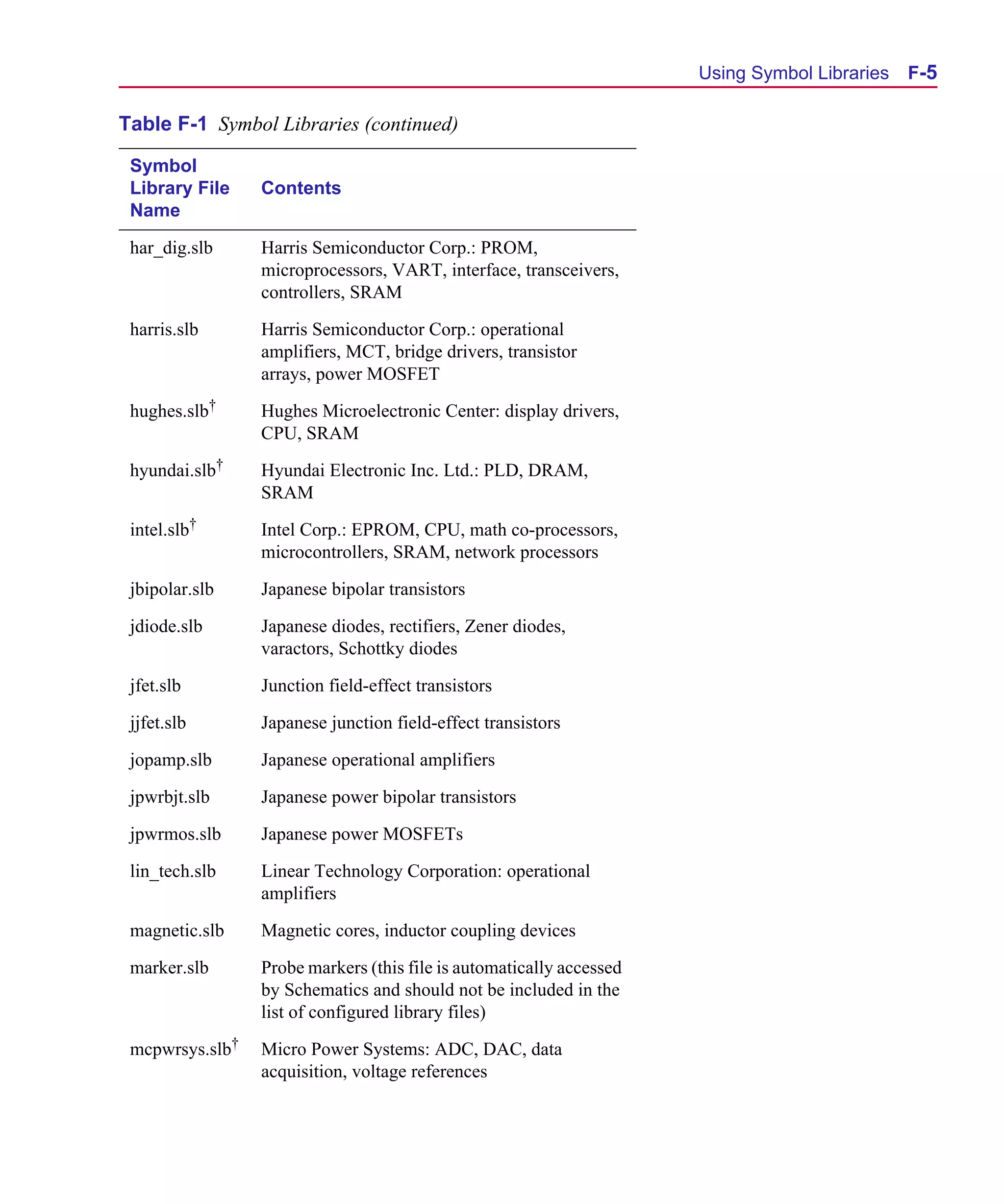
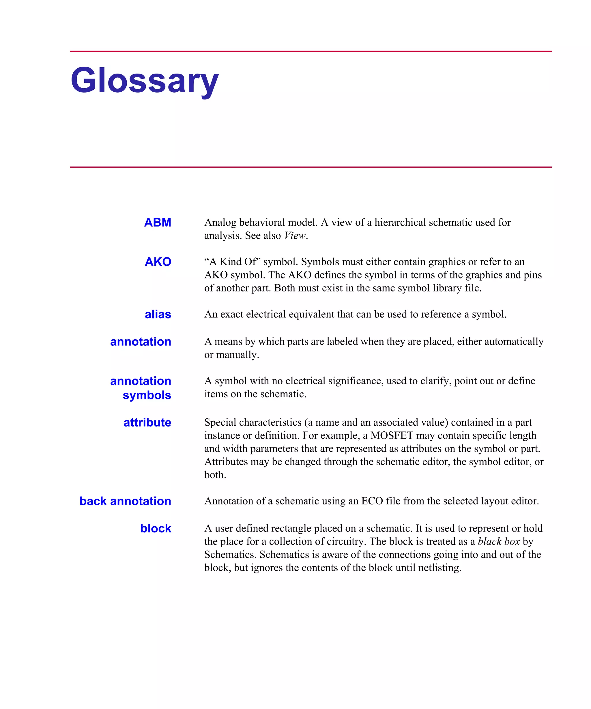
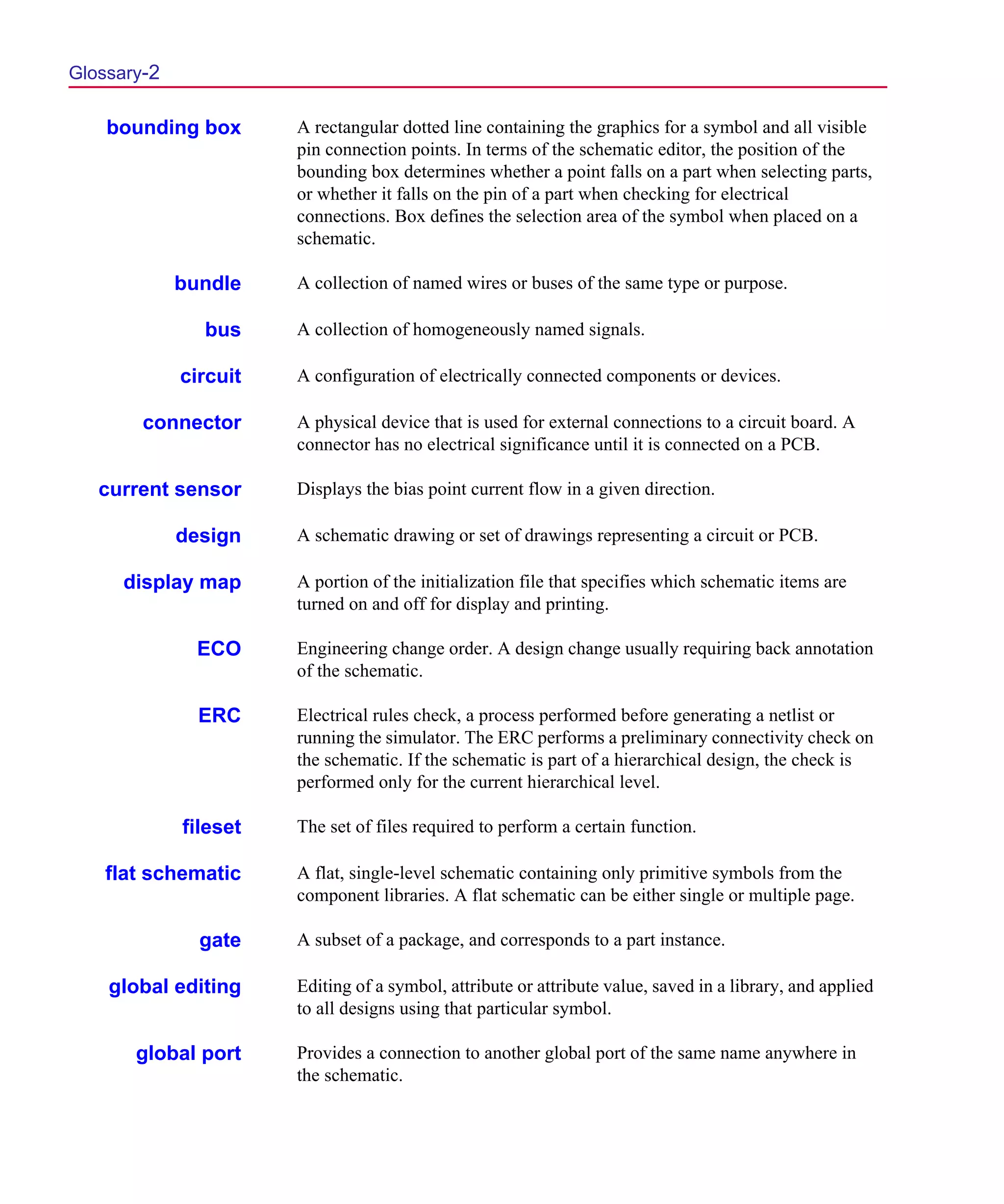
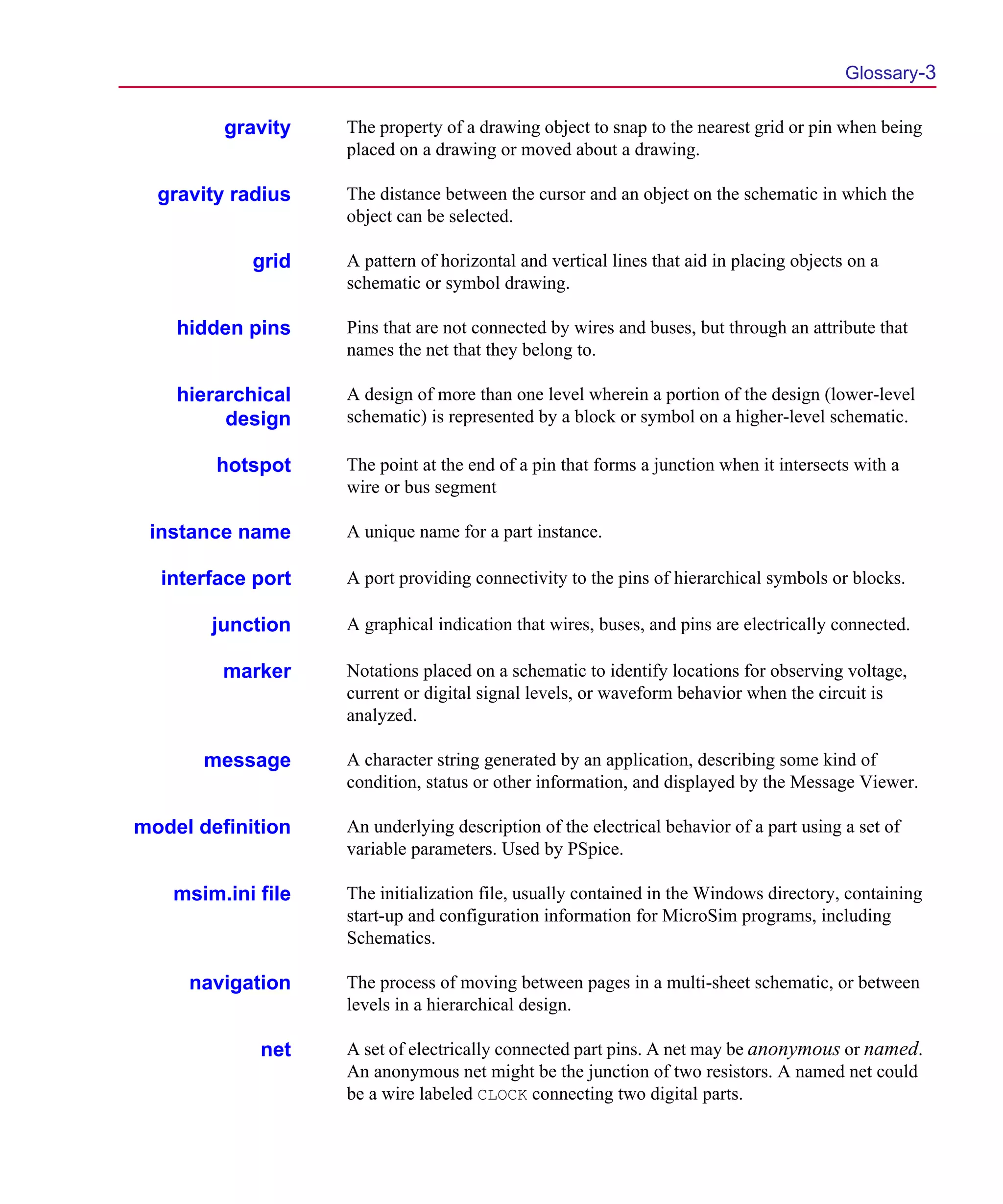
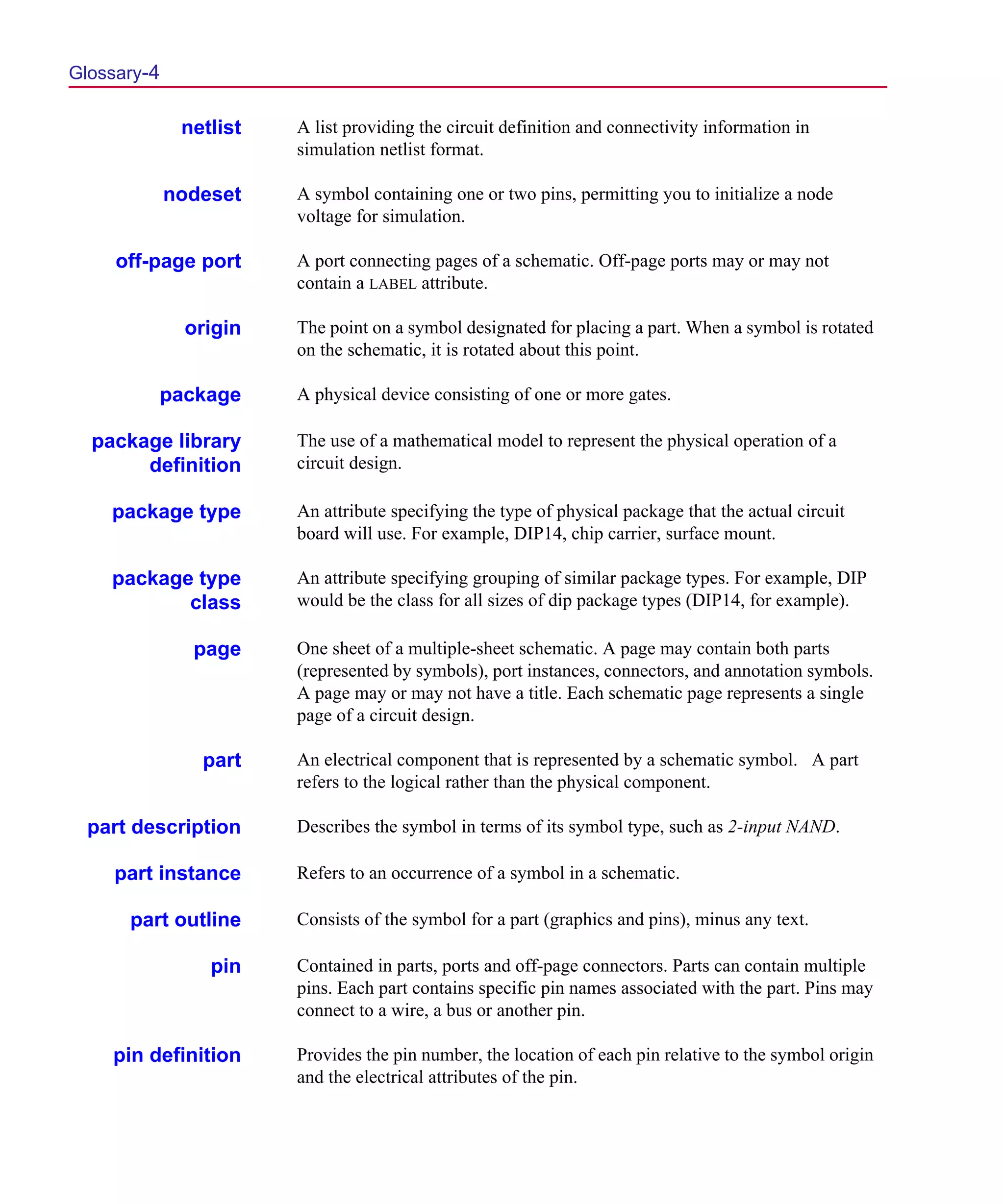
This document is the user guide for MicroSim Schematics version 8. It includes an overview of the software, instructions for getting started with drawing schematics, using the design manager to organize files, and details on using the schematic editor interface. The guide covers the main components of schematic designs, navigating the main window, menus, toolbars, and keyboard shortcuts. It aims to help new users learn the basics of creating and simulating schematic designs.


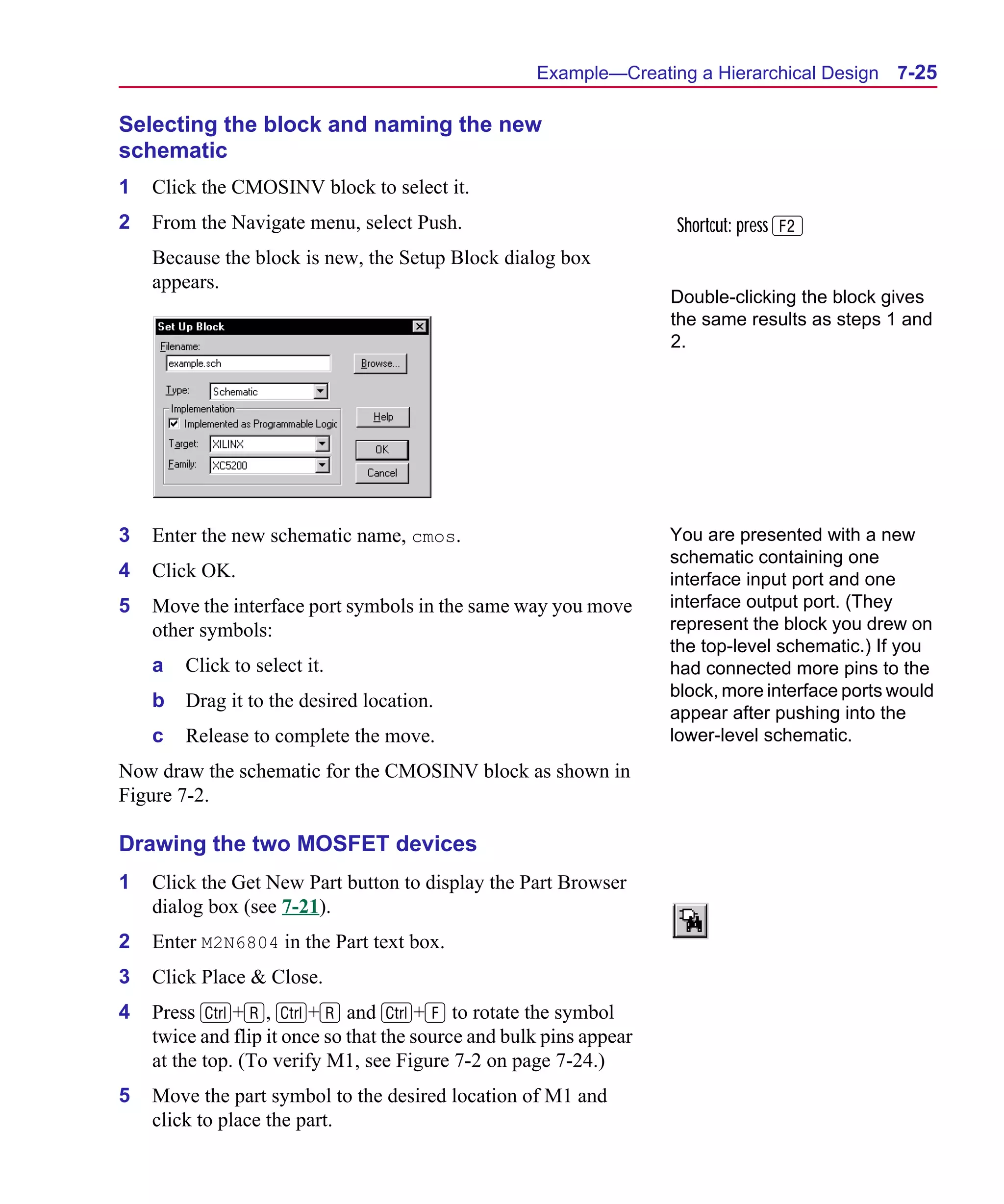
![Scug.bk : 01GETSTD.FMK Page 7 Monday, June 16, 1997 10:10 AM
Example—Drawing a Schematic 1-7
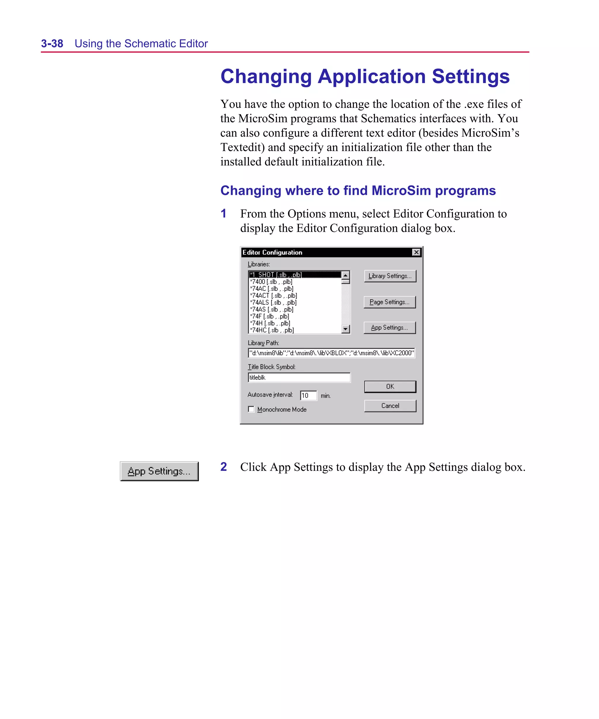
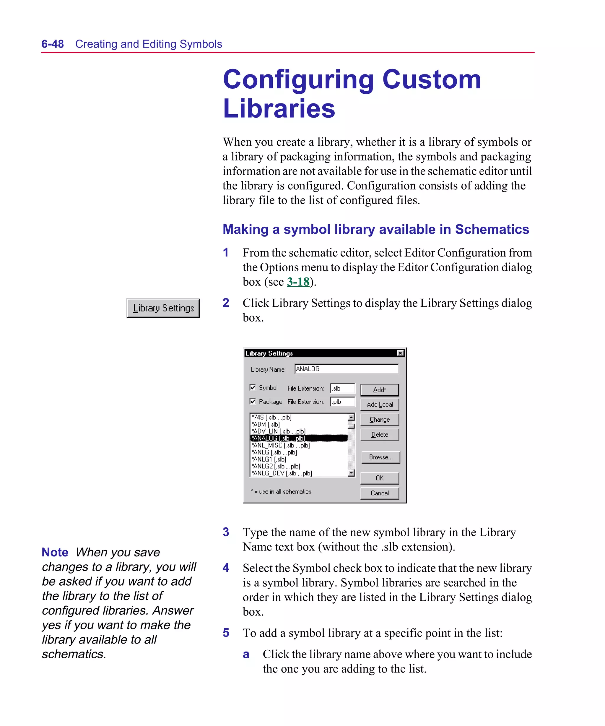
Checking Symbol Libraries
Configuration
When you installed Schematics, you selected a set of libraries to
be installed. These are global libraries, which means the
symbols contained in them are available to be used in any new
or existing schematic.
Check to see that you have the correct symbol libraries
configured for this example:
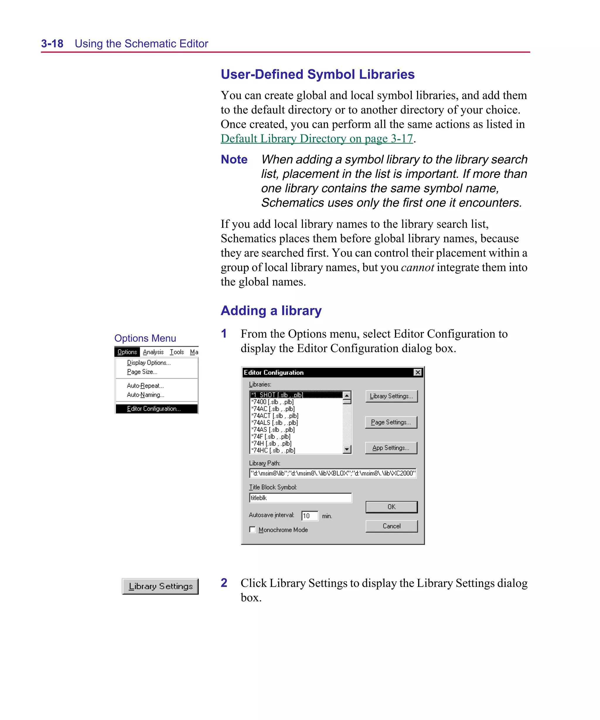
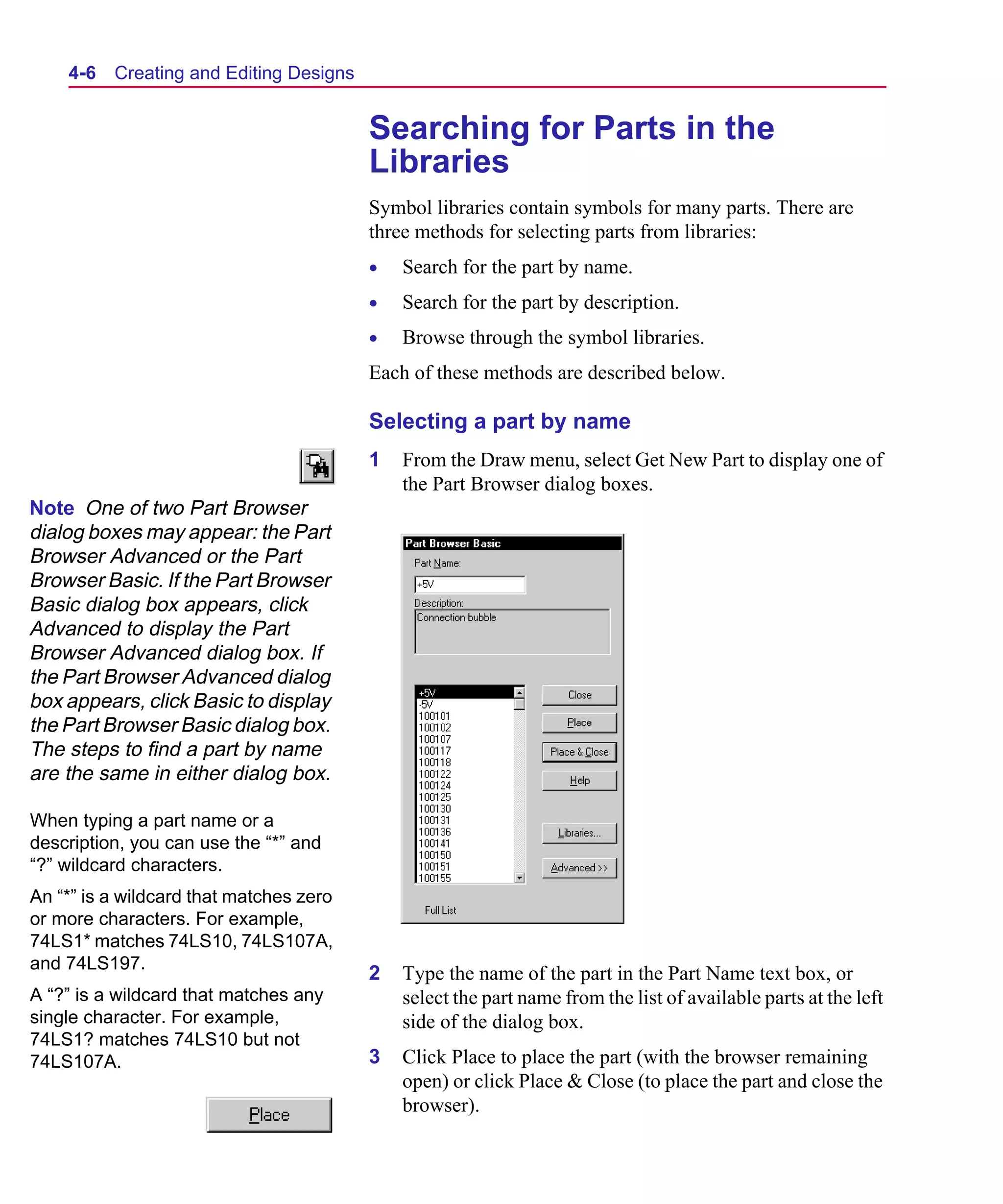
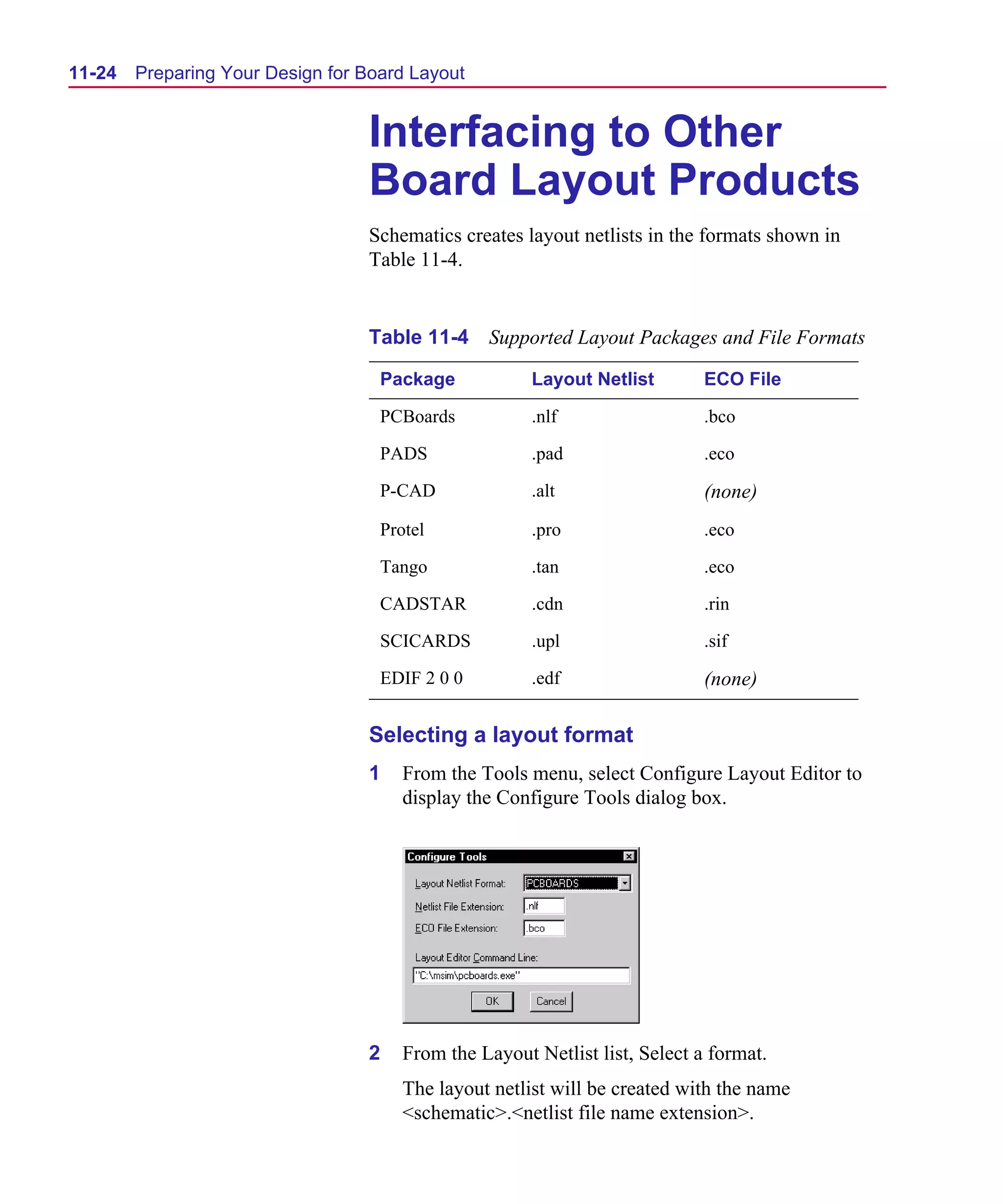
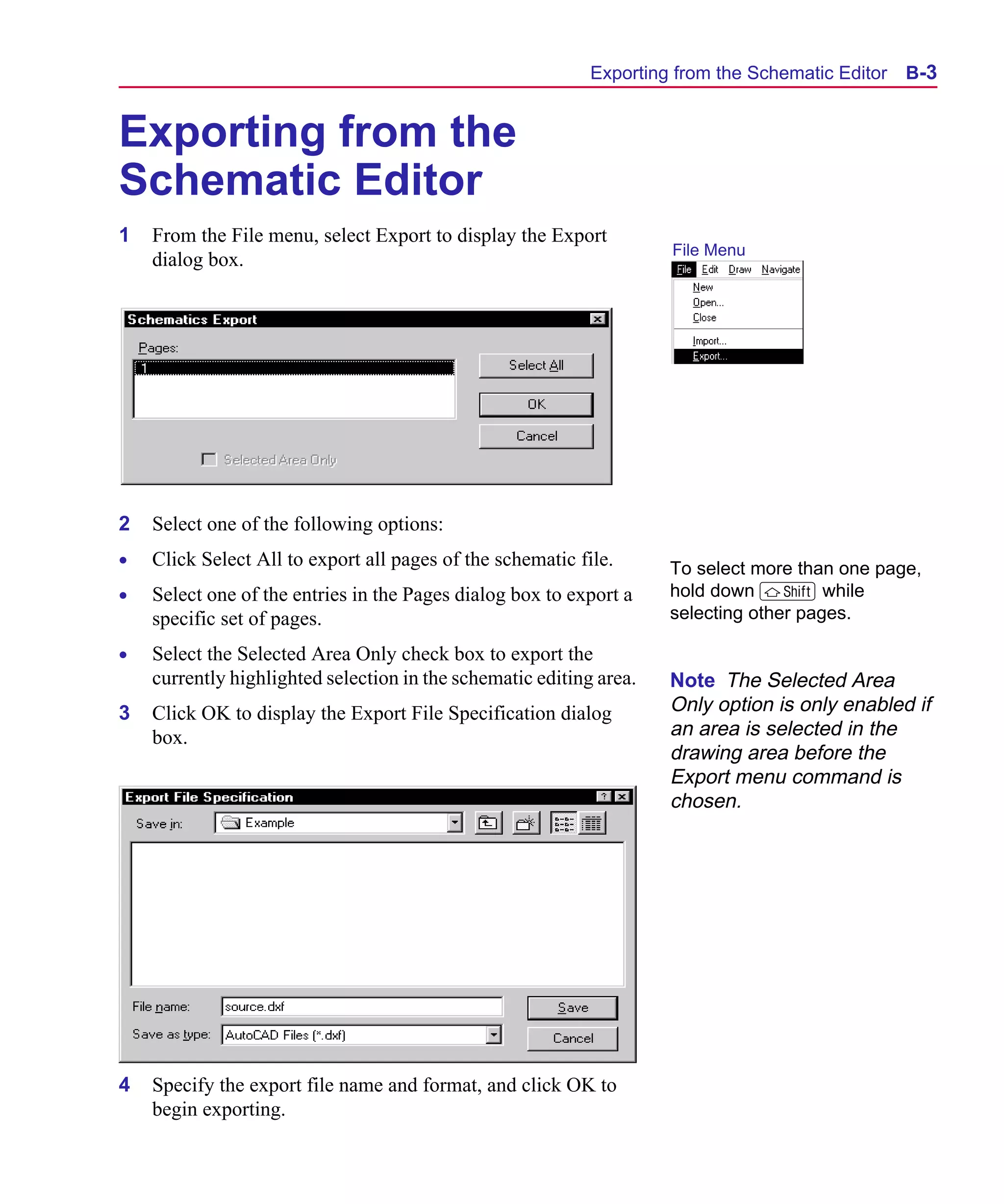
1 From the Options menu, select Editor Configuration.
2 Check that the following libraries are included in the Note If you are using the
Libraries list box: evaluation version of
Schematics, you will be using
7400 [.slb,.plb]
“eval.slb”.
analog [.slb,.plb]
opto [.slb,.plb]
port [.slb]
1_SHOT [.slb]](https://image.slidesharecdn.com/pspiceuserguideingles-121129031011-phpapp02/75/Pspice-userguide-ingles-29-2048.jpg)
![Scug.bk : 01GETSTD.FMK Page 12 Monday, June 16, 1997 10:10 AM
1-12 Getting Started
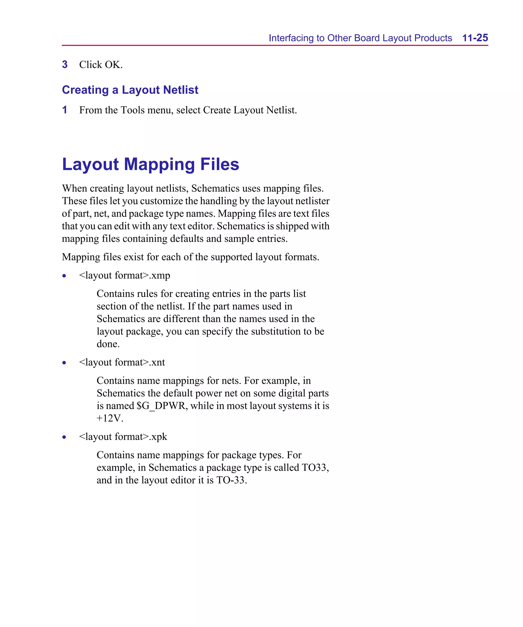
Buses must be labeled.
Examples of legal bus names
Drawing and Labeling Buses
are: Draw the bus labeled DB[1-12].
DB[0-12]
DB[0:12] Drawing the bus
DB[0..12]
DB0, DB1, CLK 1 Click the Draw Bus button.
The pointer is now shaped like a pencil (as it was when you
were drawing wires).
2 Click where you want to start the bus.
3 Click the pointer where you want to end the bus.
4 Right-click to stop drawing buses.
Labeling the bus
1 Double-click any segment of the bus to display the Set
Attribute Value dialog box.
2 Type DB[1-12] in the LABEL text box.
3 Click OK.
Connecting wires to the bus
You can use the Auto-Repeat
function to place the wires that 1 From the Options menu, select Auto-Repeat to display the
connect the pins to the bus Auto-Repeat dialog box.
because the wires will be the a Set the Vertical Offset to 00.10.
same length and fixed distances.
b Ensure that Enable Auto-Repeat is enabled.
c Click OK.
2 Click the Draw Wire button and draw a wire from pin 2 of
U5 to the bus.
3 Press M five times to place five more wires.
4 Click the Draw Wire button and draw a wire from pin 2 of
U6 to the bus.
5 Press M five times to place five more wires.](https://image.slidesharecdn.com/pspiceuserguideingles-121129031011-phpapp02/75/Pspice-userguide-ingles-34-2048.jpg)


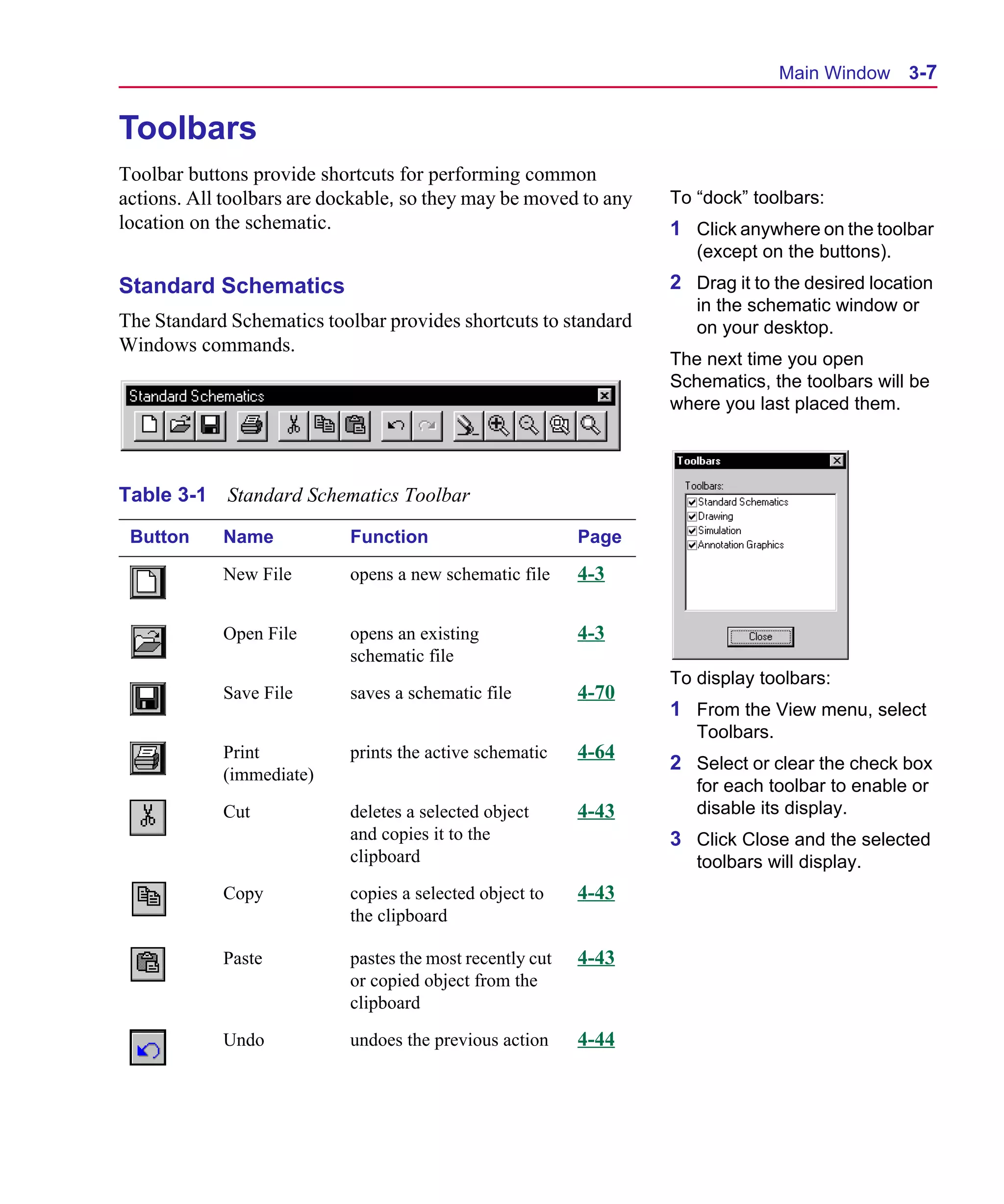


![Scug.bk : 03USESCD.FMK Page 41 Monday, June 16, 1997 10:10 AM
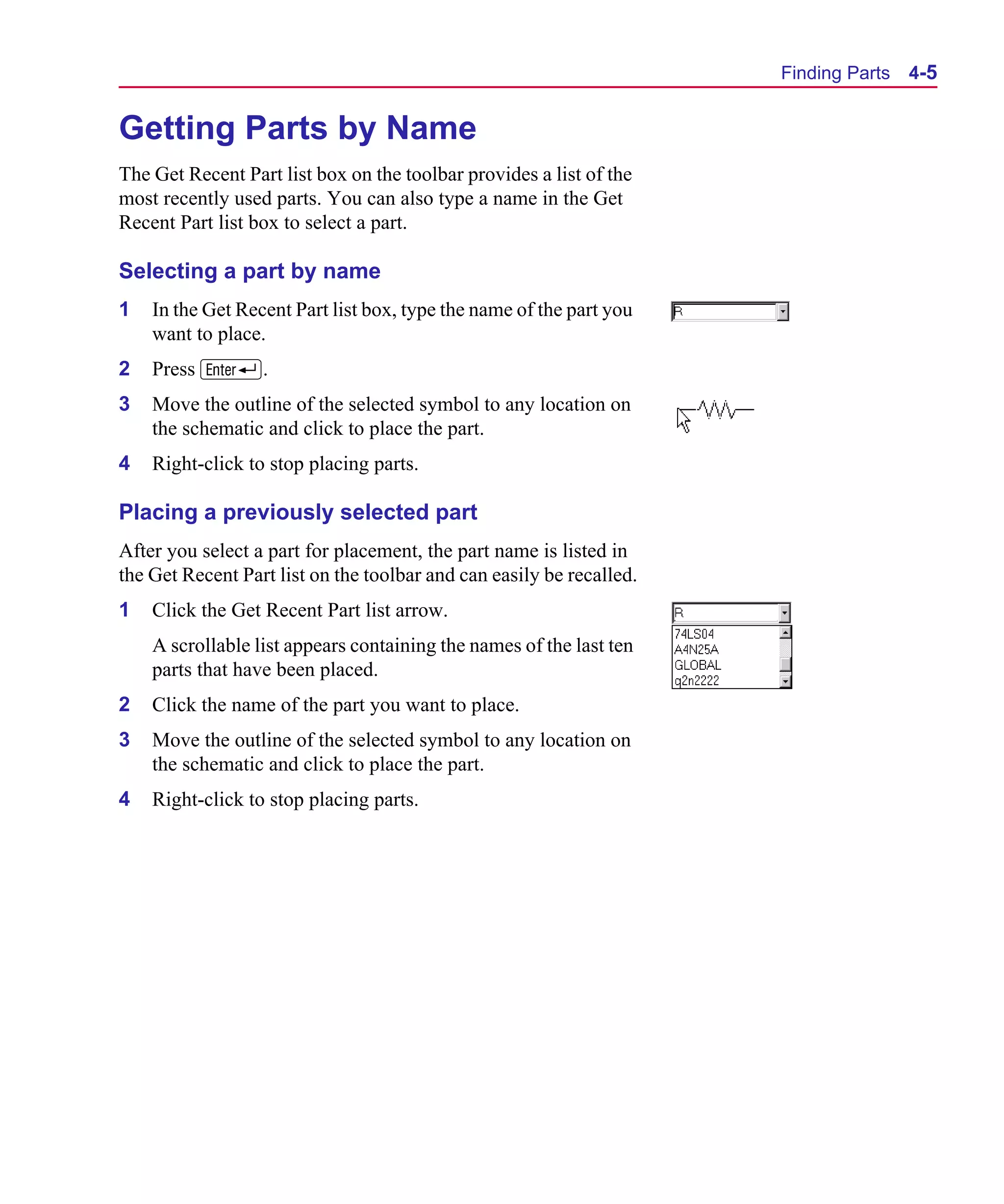
Controlling the Display in Schematics 3-41
Changing the Get Recent Part
List Size
The Get Recent Part list box on the toolbar contains a scroll-
down list of recently placed parts. The default length of this list
is ten items.
To change the length of the list, use a text editor to edit the
MRPLISTSIZE item in the [SCHEMATICS] section of the
msim.ini file.
MRPLISTSIZE=<length of list>](https://image.slidesharecdn.com/pspiceuserguideingles-121129031011-phpapp02/75/Pspice-userguide-ingles-88-2048.jpg)


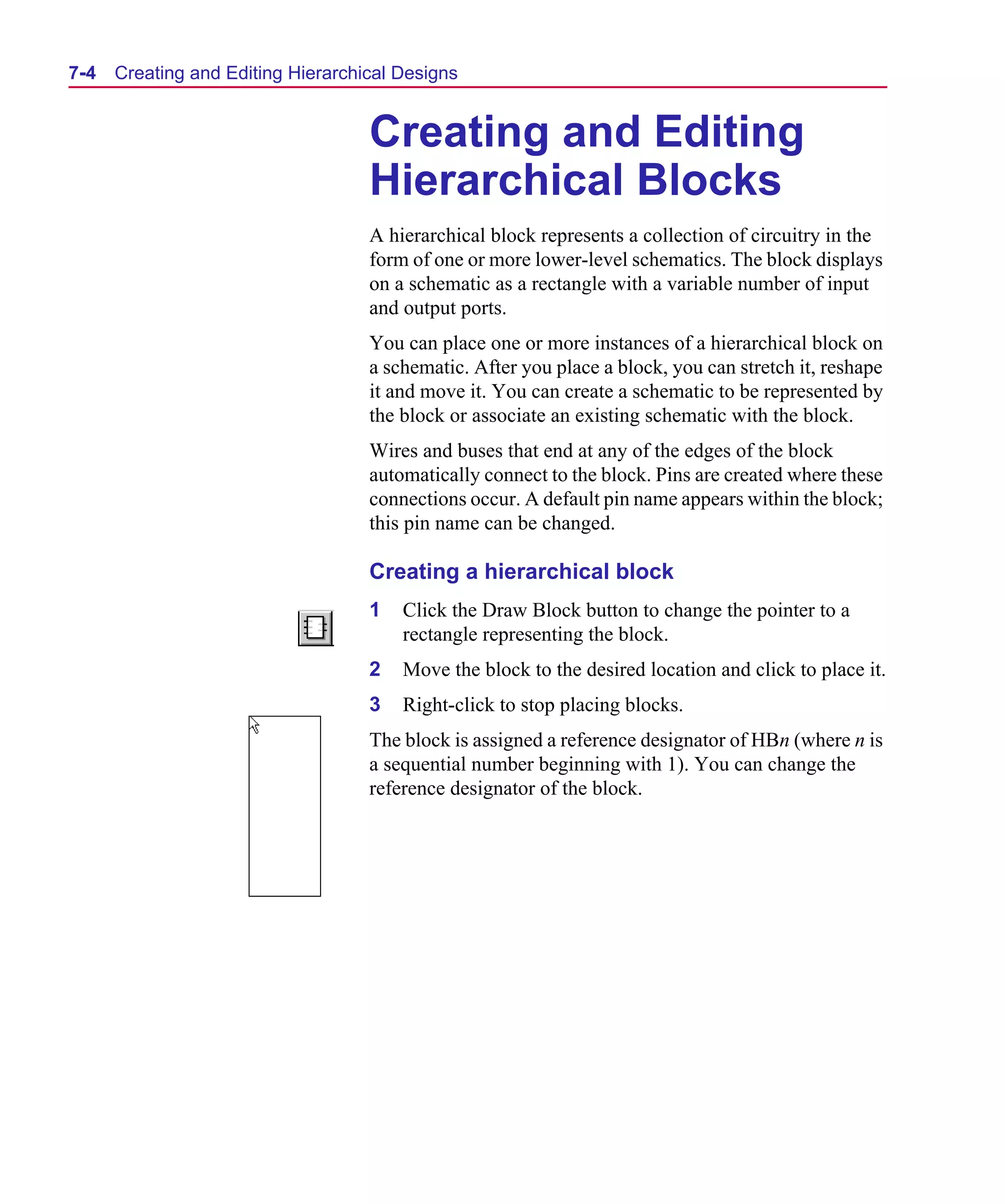
![Scug.bk : 04DESGNS.FMK Page 23 Monday, June 16, 1997 10:10 AM
Placing and Editing Parts 4-23
Drawing the first wire segment connecting the
part to the bus
1 Click the Draw Wire button.
2 Move the pencil-shaped pointer to a point on the bus where
wire segment A[0] attaches to the bus. Click to start drawing
the wire.
3 Move to pin D1 on U1 and double-click.
Using Auto-Repeat to create the remaining wire
segments
1 Enable Auto-Repeat (see Automatically repeating part
placements on page 4-19).
2 Set the horizontal offset to 00.00 and the vertical offset to
00.10.
3 Press M seven times to draw seven additional wire
segments.
Using Auto Naming to quickly label the wire
segments
1 From the Options menu, select Auto Naming to display the
Auto Naming dialog box.
2 In the Wire/Port Labels frame, select the Enable Auto-
Increment check box.
3 Type A[0] in the Label Template text box.
4 Click OK.
5 Select the first wire to be labeled.
6 From the Edit menu, select Label to label the wire. Shortcut: press C+E
7 To label each of the remaining wire segments:
a Select the wire.
b Press M.](https://image.slidesharecdn.com/pspiceuserguideingles-121129031011-phpapp02/75/Pspice-userguide-ingles-119-2048.jpg)

![Scug.bk : 04DESGNS.FMK Page 30 Monday, June 16, 1997 10:10 AM
4-30 Creating and Editing Designs
4 Double-click to place the last vertex and stop rewiring.
Drawing and Labeling Buses
Note Buses must be labeled. The connectivity of buses and bus segments in Schematics is
controlled by labeling. The rules of connectivity are:
• A bus label specifies the signals it carries and the order of
the signals.
• A bus can connect to another bus only if one is a subset of
the other (such as A[0-31] and A[16-31]).
• A bus electrically connects to a pin of a part or port if the pin
name indicates the same number of signals. Connection is in
the order specified; for example, a bus labeled A[31-0]
connected to a port labeled Addr[32-63] will electrically
connect A[31] with Addr[32], A[30], with Addr[33], and so
on.
• For a wire to be connected to a bus, the wire must be labeled
with one of the signals on the bus.
• Valid syntax for labeling a bus is:
CLK[0-15]
CLK[0:15]
CLK[0..15]
CLK[0-3, 12-15]
CLK1, CLK2, data1, data2, input,...
In the latter form, each and every signal in the bus must be
included in the series. The signals are separated by commas.](https://image.slidesharecdn.com/pspiceuserguideingles-121129031011-phpapp02/75/Pspice-userguide-ingles-126-2048.jpg)
![Scug.bk : 04DESGNS.FMK Page 31 Monday, June 16, 1997 10:10 AM
Using Wires and Buses 4-31
Drawing a bus
1 Click the Draw Bus button to change the pointer to a pencil
shape.
2 Click to start the bus.
3 Click at each vertex of the bus.
4 Right-click to end the bus and change the pencil back to a
pointer.
Labeling a bus
1 Double-click the bus segment to display the Set Attribute
Value dialog box (see 4-29).
2 Type the label in the LABEL text box.
3 Click OK.
Editing a bus label
1 Double-click the bus (or the label) to display the Set
Attribute Value dialog box (see 4-29) and the existing label
in the LABEL text box.
2 Edit the existing label or delete it and type in a new label.
Connecting wires to buses
1 Draw a wire so that it ends on the bus.
2 Label the wire with one of the signals on the bus. For
example, you can label the wire DB[12] or DB12 if the bus
is labeled DB[0:16].
Splitting buses
Connecting a bus segment to the middle of another bus segment
creates a junction. The bus segments become part of the same
bus unless labeled differently. This allows sub-buses to be taken
off a main bus, for example A[0-7] from A[0-31].
1 Draw a bus segment and end it on the main bus.
2 Label the bus segment with a subset of the signals on the
main bus.](https://image.slidesharecdn.com/pspiceuserguideingles-121129031011-phpapp02/75/Pspice-userguide-ingles-127-2048.jpg)
![Scug.bk : 04DESGNS.FMK Page 32 Monday, June 16, 1997 10:10 AM
4-32 Creating and Editing Designs
For example, you can label the bus segment DB[0:8] if the
main bus is labeled DB[0:16].
Automatically Labeling Wires
and Buses
Use the Auto Naming function to set up the labeling of wires and
ports. The syntax specified in the Label Template text box
allows you to name a uniform collection of wires.
Naming a collection of wires connected to a bus
1 From the Options menu, select Auto Naming to display the
Auto Naming dialog box.
2 In the Wire/Port Labels frame, select the Enable Auto-
Increment check box.
3 In the Label Template text box, type the label for the first
wire in the series, for example, CLK[0]. Wires will be
labeled incrementally in the order selected, as CLK[0],
CLK[1], CLK[2], and so on.
4 Click OK.
5 Select the first wire to be labeled.
Shortcut: press C+E 6 From the Edit menu, select Label to label the wire.
7 To label each of the remaining wires in the series:
a Select the wire.
b Press M.](https://image.slidesharecdn.com/pspiceuserguideingles-121129031011-phpapp02/75/Pspice-userguide-ingles-128-2048.jpg)


![Scug.bk : 05SYMBED.FMK Page 10 Monday, June 16, 1997 10:10 AM
5-10 Using the Symbol Editor
Title Bar
The symbol editor window title bar displays the name of the
symbol library and the symbol currently being edited. For
example:
[C:MSIMLIBPORT.SLB:GLOBAL]
When you open a symbol editor window and have not specified
a symbol for editing, the title bar displays:
<new>:<new>
This indicates you are editing a new symbol in a new library.](https://image.slidesharecdn.com/pspiceuserguideingles-121129031011-phpapp02/75/Pspice-userguide-ingles-176-2048.jpg)


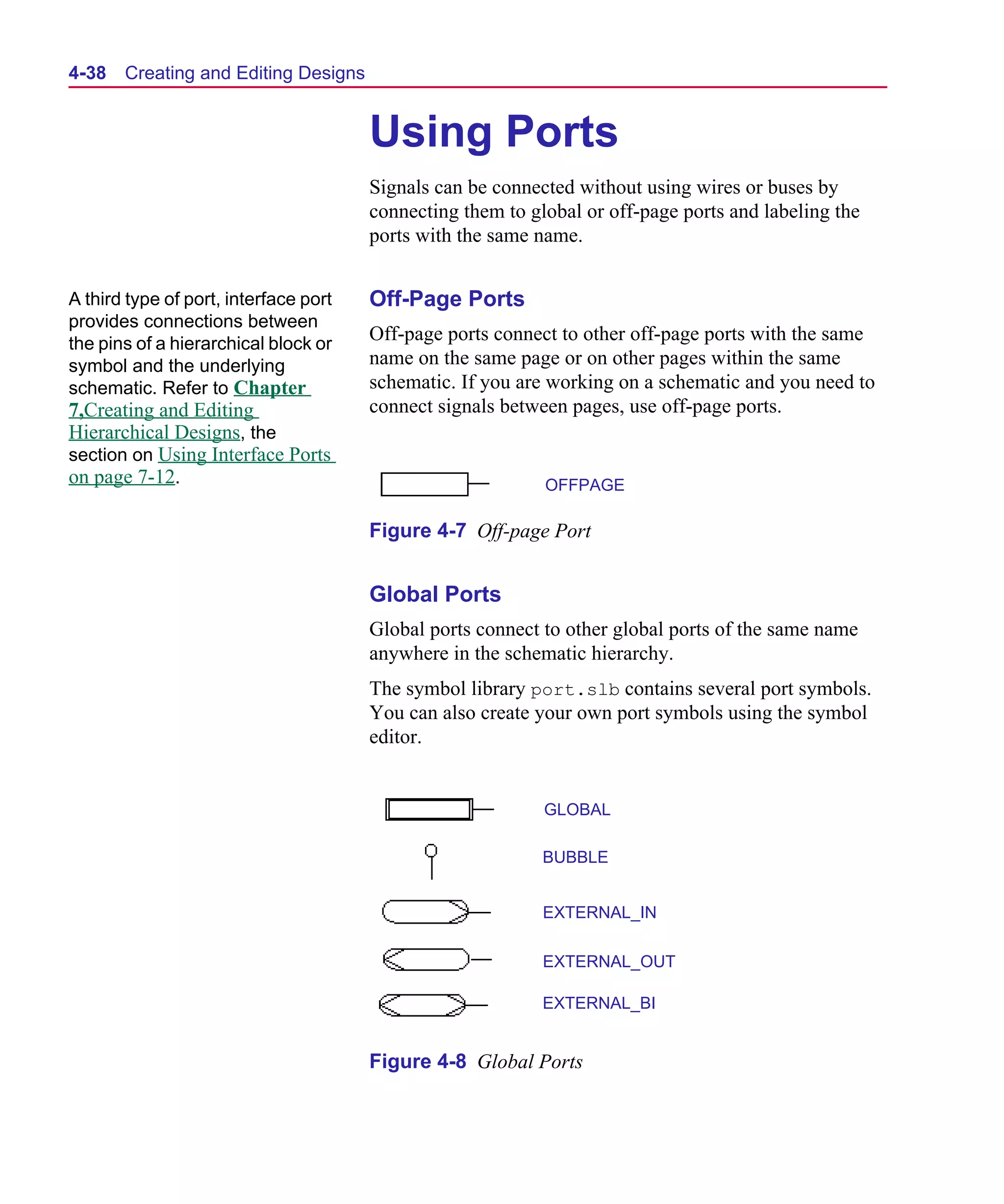
![Scug.bk : 07HIERCH.FMK Page 12 Monday, June 16, 1997 10:10 AM
7-12 Creating and Editing Hierarchical Designs
Using Interface Ports
When you use a block or symbol to represent an underlying
schematic, connections to the underlying schematic are made by
means of the pins on the block or symbol. The pins on the block
or symbol must correspond to interface ports placed on the
underlying schematic, that is, for each pin there must be a
corresponding interface port with the same name as the pin.
If a bus is connected to the block or symbol, the pin name must
indicate the number of signals, such as, CLK[0:3]. The interface
port would have the same name, such as, CLK[0:3].
If you make changes to the pins on a block or symbol, you must
make the corresponding changes on any underlying schematics
it represents.
If you... You Must...
add a pin add an interface port with the same name
as the pin.
delete a pin delete the corresponding interface port.
change the name of a change the label of the corresponding
pin interface port.
There are three interface port symbols available in “port.slb”:
IF_IN
IF_OUT
INTERFACE
You can use the symbol editor to create custom interface ports.](https://image.slidesharecdn.com/pspiceuserguideingles-121129031011-phpapp02/75/Pspice-userguide-ingles-257-2048.jpg)


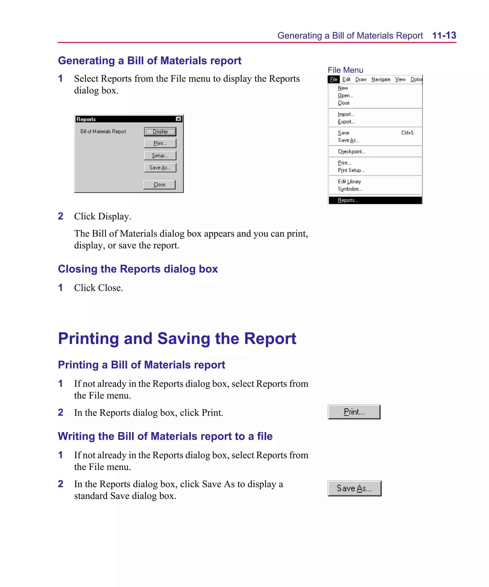
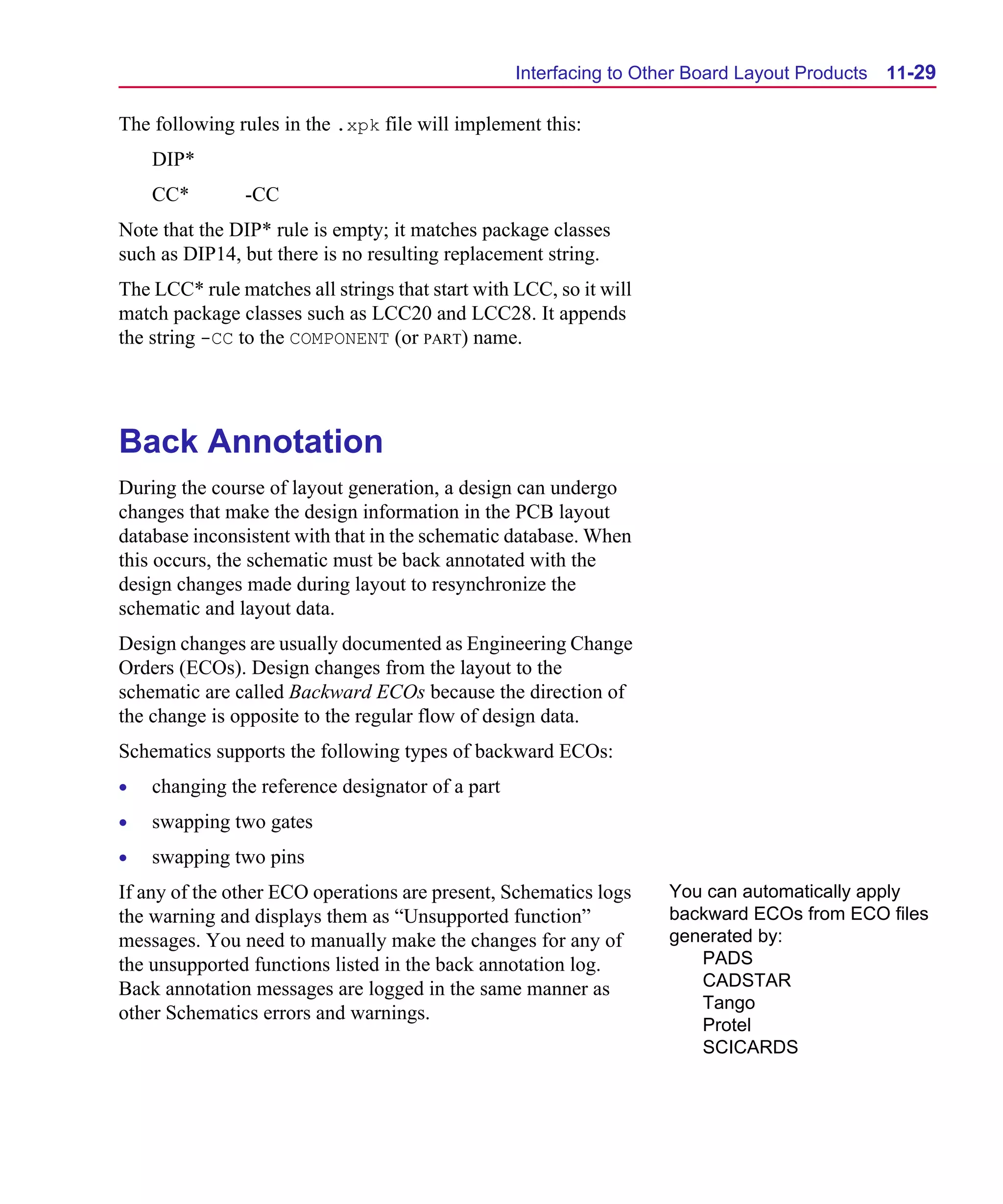
![Scug.bk : 11LAYOUT.FMK Page 14 Monday, June 16, 1997 10:10 AM
11-14 Preparing Your Design for Board Layout
Customizing the Format of the
Report
1 Click Setup to display the Report Setup dialog box.
2 In the Format text box, type the attributes to be displayed in
the report according to the following syntax:
[descriptive text]@<attribute name>
where the ‘@’ sign indicates value substitution for the
named attribute. Specify multiple attributes by using the
preceding syntax in a comma-separated list. For example,
you could specify that the part instance VALUE attribute, and
your own user defined attributes, COST and ADDR, be
reported by typing the following into the Format text box:
value = @VALUE, cost = @COST, address =
@ADDR
3 In the Component Description File text box, enter the name
of the component description file (.cdf) to be used.
4 Choose a Print Output format.
Choose Text to format the Bill of Materials report in ASCII
format with one entry per component type.
5 Click OK.](https://image.slidesharecdn.com/pspiceuserguideingles-121129031011-phpapp02/75/Pspice-userguide-ingles-305-2048.jpg)


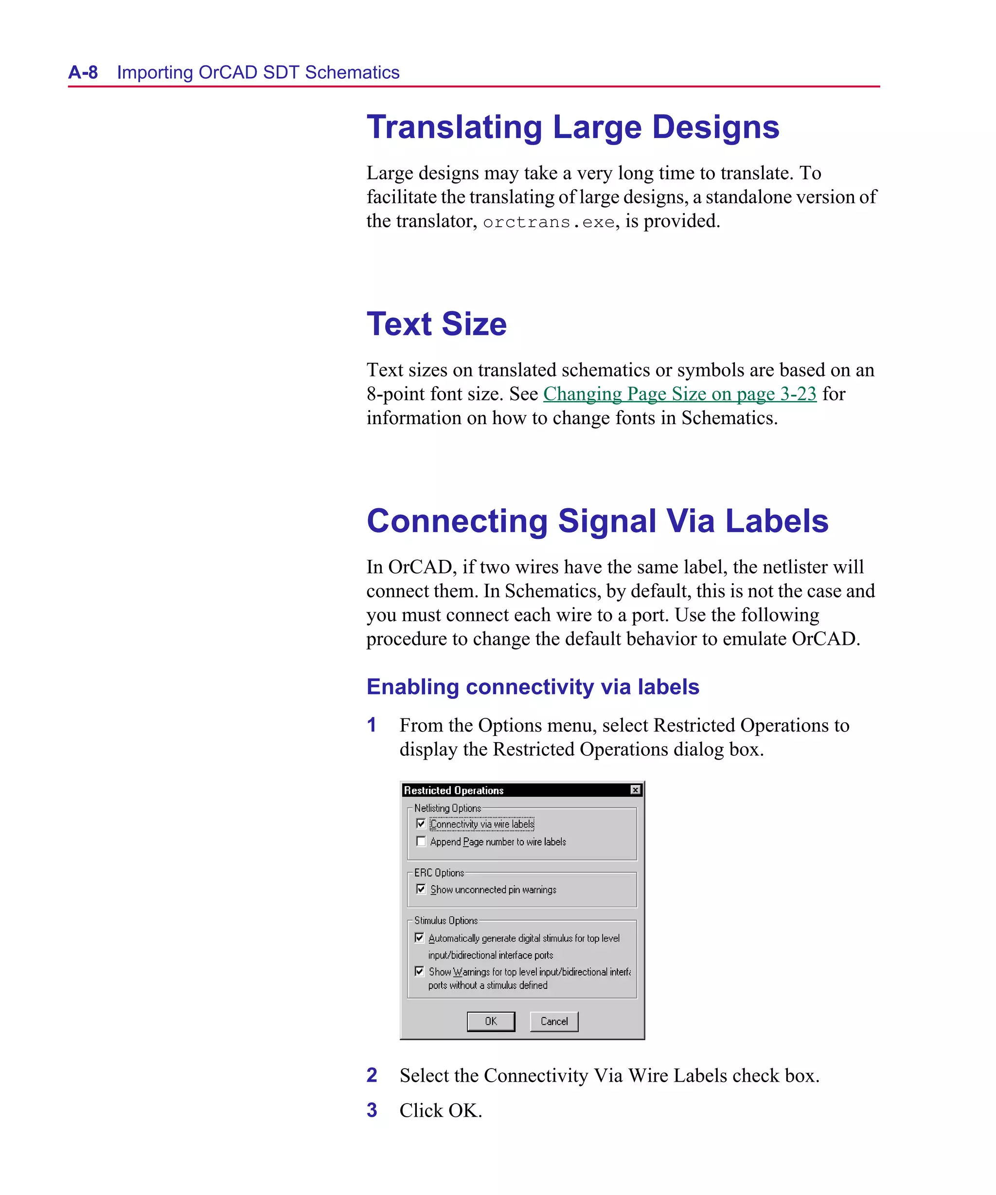
![Scug.bk : A-ORCAD.FMK Page 10 Monday, June 16, 1997 10:10 AM
A-10 Importing OrCAD SDT Schematics
• Wires that cross pins exactly at the pin hotspot are translated
as connected.
• Unlabeled wires connected to buses are translated as
unconnected wires, that is, they are not connected to the bus.
• Wires and buses in Schematics can only have a single label.
Any connections, bus mapping or splitting that use the
OrCAD multiple label feature will not translate correctly. In
Schematics, you will need to manually reconnect these
wires and buses.
In Schematics, you can split a bus directly by labeling the
subbus with a subset of the signals on the main bus. For
example, if the main bus is data[0..15], you can connect a
bus to it and label it data[0..7] and connect this directly to a
port or pin with a name of the same width, such as,
inputData[0..7]. (See Splitting buses on page 4-31.)
• By default, Schematics does not consider wires with the
same label to be connected unless they are drawn as
connected. You must connect them to offpage ports or
enable the Connectivity Via Labels option.
To change the default, see Enabling connectivity via labels
on page A-8.
Simulation
• Simulation attributes that are added to symbols are based on
information from the OrCAD SDT standard libraries.
Therefore, pin name references in these attributes can be
incorrect if a part (such as user-drawn) is being used that has
the same name as another part (from the standard libraries,
for example) on the schematic.](https://image.slidesharecdn.com/pspiceuserguideingles-121129031011-phpapp02/75/Pspice-userguide-ingles-331-2048.jpg)


![Scug.bk : D-ADNET.FMK Page 2 Monday, June 16, 1997 10:10 AM
D- 2 Advanced Netlisting Configuration Items
Specifying PSpice Node
Name Netlisting
Preferences
By default, the PSpice netlister assigns names such as $N_001
to nodes that are not explicitly labeled.
You can change the format that the netlister uses to create these
names by using a text editor and editing the msim.ini file in the
Windows directory. Add a line to the [SCHEMATICS] section
in the form:
nltemplate=<prefix>%[minimum width]ld
The default value is:
nltemplate=$N_%04ld
The term ld must be in lowercase.
If [minimum width] begins with a zero, leading 0’s are added if
the number of characters in the node number is less than the
minimum width. For example, N%ld would create node
numbers N1, N2, N3 instead of $N_001, $N_002, $N_003.](https://image.slidesharecdn.com/pspiceuserguideingles-121129031011-phpapp02/75/Pspice-userguide-ingles-344-2048.jpg)

![Scug.bk : D-ADNET.FMK Page 4 Monday, June 16, 1997 10:10 AM
D- 4 Advanced Netlisting Configuration Items
Customizing EDIF
Netlists
You can change the amount each level in the netlist is indented
by changing the EDIFINDENT item in the [SCHEMATICS]
section of the msim.ini initialization file. Use a text editor to
edit the msim.ini file in the Windows directory.
EDIFINDENT specifies the character to use to indent each level
in an EDIF netlist.
The default is:
EDIFINDENT=”” ““](https://image.slidesharecdn.com/pspiceuserguideingles-121129031011-phpapp02/75/Pspice-userguide-ingles-346-2048.jpg)


![2711e um006 -en-p[1]](https://cdn.slidesharecdn.com/ss_thumbnails/2711e-um006-en-p1-120514065850-phpapp02-thumbnail.jpg?width=640&height=640&fit=bounds)


