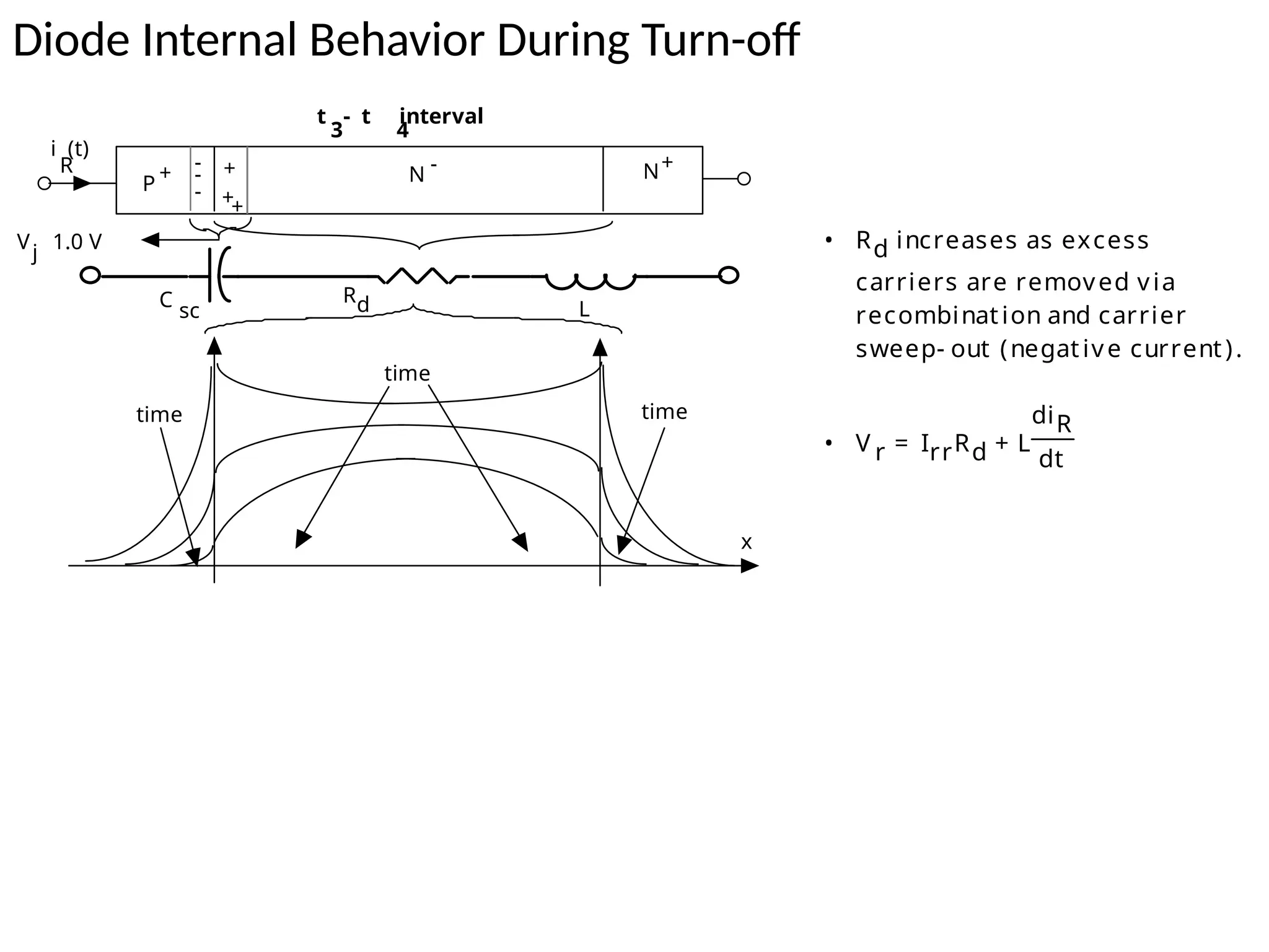
• Thyristor devices can convert and control large amounts of power in AC or DC systems while using
very low power for control.
• Thyristor family includes
1
Power Semiconductor Switches
Power Diodes
3 layer device
Power Transistors
4layer Device
Thyristors
4 layer Device
Thyristor Family
Sillicon Controlled
Rectifier Gate Turn off SCR Triac / Diac
SCS/MCT
Ideal and Practical Switch
• Ideal Switch Characteristics
 Zero on-state resistance – No
forward voltage drop when on
 Infinite off-state resistance –
No leakage current when off
 Current limitless when on-
either direction – Conduction
current a function of external
components only
 No limit on amount of voltage
across switch when off –
Blocking voltage infinite
(forward or reverse)
 Switch can transition from on-
off or off-on instantaneously
+ v -
Continue
• Practical Switch -real world”
switch is not ideal
 Limited conduction current when the
switch on, limited blocking voltage
when the switch is in the off
 Both are directional in practical
switch
 Limited switching speed that caused
by the finite turn on and turn-off
times
 Finite, nonzero on-state and off-state
resistances-There is a I2
R loss when
on and some leakage when off (very
small)
 Voltage and current transition is
not abrupt
Characteristics of Controllable Switch
4
Power diodes
Basic Features
• Large Breakdown volatge
• Low on state voltage and resistance
• Fast turn on and fast turn off ,
• Large power dissipation capabilities
6
Trade off
• Break down voltage and on state losses - width of drift region 
Break down voltage  on state resistance 
• On state losses and switching Frequency –on state losses 
temperature of device  Carrier life time (for high current device)

storage delay time limits switching frequency
• But larger Carrier life time reduces on state losses
Recombination
• Life time of carrier is constant ? Most of case considered as constant
for material
• Power Semiconductor Life time of carrier varies with device
operating condition , can be increase or decrease but it has impact
on on state losses and switching losses
• Life time increases with increase internal temperature of device This
will lead increase switching time of device – increase in storage
delay time (Mainly Bipolar devices )
• Larger excess carrier density cause to decreases carrier life time .
High current device carrier life time decreases which increases on
state losses
• On state drift region voltage drop
7
8
Structure of Power diode
Ref. Mohan, N. and T. Undeland, Power Electronics: Converters,
Applications, and Design, John Wiley & Sons,Newyork, 1995.
Types of Power Diode
The physical width of the drift region (W) can be either large
or smaller than the depletion layer width at the break down
voltage. Consequently two type of diodes exist, (i) non
punch through type, (ii) punch through type.
non-punch through: depletion layer boundary doesn’t reach the
end of the drift layer.
punch through: the depletion layer spans the entire drift
region and is in contact with the n+
cathode.
However, due to very large doping density of the cathode,
penetration of drift region inside cathode is negligible.
9
Electrical Field
10
Punch Trough
Non Punch Trough
Under the assumption of uniform electric field strength it can
be shown that for the same break down voltage, the “punch
through” construction will require approximately half the drift
region width of a comparable “ non - punch through”
construction.
reduced width of the drift region in punch through diodes lowers
the on-state voltage drop for the same forward current density
compared to a non-punch through diode.
Forward bias injects holes into drift
region from P+
layer. Electrons
attracted into drift region from N+
layer. So-called double injection.
 If Wd ≤ high level diffusion length
La , carrier distributions quite flat with
p(x) ≈ n(x) ≈ na.
For na >> drift region doping Nd,
the resistance of the drift region will
be reduced to quite small. So-called
conductivity modulation.
• On-state losses greatly reduced
below those estimated on basis of drift
region low-level (Nd) ohmic
conductivity.
P
+
N+
p (x)
n
x
n
po
x
-
+
N
-
n =
no 10
14
p =
no
10 6
p
no
p(x) = n(x)
= n = 10
a
16
n (x)
p
W
d
log scale
Conductive Modulation of Drift region
Drift Region On-State Voltage Estimate
• IF =

F
Q
=

na
A Wd
q ; Current needed
to maintain stored charge QF.
• IF =
q [µn + µp] na A Vd
Wd
;
Ohm’s Law (J = E)
• Vd =
Wd
2
[µn + µp] 
; Equate above
two equations and solve for Vd
• Conclusion: long lifetime  minimizes Vd.
Diode Switching Waveforms in Power Circuits
I F
I
t
d i / d t
F d i / d t
R
V
r r
t
t
t
1
2
3
t
5
V
FP
t
V on
0.25 I r r
t
rr
Q = I t / 2
rr
rr rr
t
5
t
4
S =
rr
V
R
t
4
•
diF
dt and
diR
dt determined
by external circuit.
• Inductances or power
semiconductor devices.
14
 Reverse bias voltage removed, Forward bias voltage
applied
 The space charge stored in the depletion region is
removed (discharged) because of the excess-carrier
injected from both ends of the device.
 Before the depletion layer is discharged to its thermal
equilibrium level, there is a large ohmic resistance
appears in the pn junction and produces a large voltage
drop.
 The inductance of the silicon wafer and the attached
wires also help to build up the voltage overshoot.
 Faster turn-on time can be achieved only by reducing
the carrier lifetime, which will produce a higher
forward voltage drop and higher on-state losses.
Turn On Mechanism
Diode Internal Behavior During Turn-on
P
+
N - N+
+
-
+
+
-
-
V ­1.0 V
j
time
time
time
x
t interval
2
i (t)
F
• Injection of excess
carriers into drift
region greatly
reduces Rd.
t interval
1
P
+ N
- N+
+
-
+
+
+
-
-
-
i (t)
F
Csc R d L
16
 The excess carriers stored in the drift region must be removed
before the metallurgical junction (pn junction) can become
reverse biased.
 The excess carriers are removed by the combined action of
recombination and sweep-out by negative diode current.
 The diode voltage will not change from its on-state voltage as
long as there are excess carriers at the drift region of pn
junctions.
 when the pn junction becomes reverse biased, there will be a
rapidly voltage drop on the diode voltage.
 Because of the negative diode voltage, the diode current can
not go negative further and reduced to zero. Or Insufficient
excess carriers remain to support Irr, so P+N- junction
becomes reverse-biased and current decreases to zero.
 Voltage drops from Vrr to VR as current decreases to zero
 Negative current integrated over its time duration removes a
total charge Qrr.
Turn Off Behaviour
17
When a diode is switched quickly from forward to
reverse bias, it continues to conduct due to the minority
carriers which remains in the p-n junction.
The minority carriers require finite time, i.e, trr (reverse
recovery time) to recombine with opposite charge and
neutralise.
Effects of reverse recovery are increase in switching
losses, increase in voltage rating, over-voltage (spikes) in
inductive loads
Diode Internal Behavior During Turn-off
• Rd increases as excess
carriers are removed via
recombination and carrier
sweep- out (negative current).
• V r = IrrRd + L
diR
dt
P
+ N - N+
+
-
++
-
-
V ­1.0 V
j
time
time time
x
i (t)
R
t - t interval
3 4
L
Rd
C
sc
Factors Effecting Reverse Recovery Time
• Irr =
diR
dt
t4 =
diR
dt
trr
(S + 1)
; Defined on
switching waveform diagram
• Qrr =
Irr trr
2
=
diR
dt
trr
2
2(S + 1)
; Defined
on waveform diagram
• Inverting Qrr equation to solve for trr yields
trr =
2Qrr(S+1)
diR
dt
and Irr =
2Qrr
diR
dt
(S + 1)
• If stored charge removed mostly
by sweep-out Qrr ≈ QF ≈ IF 
• Using this in eqs. for Irr and
trr and assuming S + 1 ≈ 1
gives
trr =
2 IF 
diR
dt
and
Irr = 2 IF 
diR
dt
S shapiness factor
21
Types of Power Diodes
Line frequency (general purpose):
On state voltage: very low (below 1V)
Large trr (about 25us) (very slow response)
Very high current ratings (up to 5kA)
Very high voltage ratings(5kV)
Used in line-frequency (50/60Hz) applications such as rectifiers
Fast recovery
Very low trr (<1us).
Power levels at several hundred volts and several hundred amps
Normally used in high frequency circuits inverter fed drives etc
Schottky
Very low forward voltage drop (typical 0.3V)
Limited blocking voltage (50-100V)
Used in low voltage, high current application such as switched mode
power supplies.
22
Types of Power Diodes
Line frequency (general purpose):
On state voltage: very low (below 1V)
Large trr (about 25us) (very slow response)
Very high current ratings (up to 5kA)
Very high voltage ratings(5kV)
Used in line-frequency (50/60Hz) applications such as rectifiers
Fast recovery
Very low trr (<1us).
Power levels at several hundred volts and several hundred amps
Normally used in high frequency circuits inverter fed drives etc
Schottky
Very low forward voltage drop (typical 0.3V)
Limited blocking voltage (50-100V)
Used in low voltage, high current application such as switched mode
power supplies.
24
References
1.Benjamin Streetman Semiconductor Physics
2. Ned Mohan, Tore M. Undeland, William P. Robbins, “Power Electronics,
Converters, Application and Design” John Wiley & Sons(Asia), Publishers.
Third Edition 2003.
3.P. C. Sen, “Power Electronics” Tata McGraw Hill Publishing Company
Limited, New Delhi, 1987
4http://ece- www.colorado.edu/~bart/book/book/title.htm11/10/2004 16:07:51
Power Diode
25
Three Layer devices , middle layer is drift region , lightly doped and break
down voltage depends on middle layer width

power diode operation static and dynamic characterstics.pptx

  • 1.
    • Thyristor devicescan convert and control large amounts of power in AC or DC systems while using very low power for control. • Thyristor family includes 1 Power Semiconductor Switches Power Diodes 3 layer device Power Transistors 4layer Device Thyristors 4 layer Device Thyristor Family Sillicon Controlled Rectifier Gate Turn off SCR Triac / Diac SCS/MCT
  • 2.
    Ideal and PracticalSwitch • Ideal Switch Characteristics  Zero on-state resistance – No forward voltage drop when on  Infinite off-state resistance – No leakage current when off  Current limitless when on- either direction – Conduction current a function of external components only  No limit on amount of voltage across switch when off – Blocking voltage infinite (forward or reverse)  Switch can transition from on- off or off-on instantaneously + v -
  • 3.
    Continue • Practical Switch-real world” switch is not ideal  Limited conduction current when the switch on, limited blocking voltage when the switch is in the off  Both are directional in practical switch  Limited switching speed that caused by the finite turn on and turn-off times  Finite, nonzero on-state and off-state resistances-There is a I2 R loss when on and some leakage when off (very small)  Voltage and current transition is not abrupt
  • 4.
  • 6.
    Power diodes Basic Features •Large Breakdown volatge • Low on state voltage and resistance • Fast turn on and fast turn off , • Large power dissipation capabilities 6 Trade off • Break down voltage and on state losses - width of drift region  Break down voltage  on state resistance  • On state losses and switching Frequency –on state losses  temperature of device  Carrier life time (for high current device)  storage delay time limits switching frequency • But larger Carrier life time reduces on state losses
  • 7.
    Recombination • Life timeof carrier is constant ? Most of case considered as constant for material • Power Semiconductor Life time of carrier varies with device operating condition , can be increase or decrease but it has impact on on state losses and switching losses • Life time increases with increase internal temperature of device This will lead increase switching time of device – increase in storage delay time (Mainly Bipolar devices ) • Larger excess carrier density cause to decreases carrier life time . High current device carrier life time decreases which increases on state losses • On state drift region voltage drop 7
  • 8.
    8 Structure of Powerdiode Ref. Mohan, N. and T. Undeland, Power Electronics: Converters, Applications, and Design, John Wiley & Sons,Newyork, 1995.
  • 9.
    Types of PowerDiode The physical width of the drift region (W) can be either large or smaller than the depletion layer width at the break down voltage. Consequently two type of diodes exist, (i) non punch through type, (ii) punch through type. non-punch through: depletion layer boundary doesn’t reach the end of the drift layer. punch through: the depletion layer spans the entire drift region and is in contact with the n+ cathode. However, due to very large doping density of the cathode, penetration of drift region inside cathode is negligible. 9
  • 10.
    Electrical Field 10 Punch Trough NonPunch Trough Under the assumption of uniform electric field strength it can be shown that for the same break down voltage, the “punch through” construction will require approximately half the drift region width of a comparable “ non - punch through” construction. reduced width of the drift region in punch through diodes lowers the on-state voltage drop for the same forward current density compared to a non-punch through diode.
  • 11.
    Forward bias injectsholes into drift region from P+ layer. Electrons attracted into drift region from N+ layer. So-called double injection.  If Wd ≤ high level diffusion length La , carrier distributions quite flat with p(x) ≈ n(x) ≈ na. For na >> drift region doping Nd, the resistance of the drift region will be reduced to quite small. So-called conductivity modulation. • On-state losses greatly reduced below those estimated on basis of drift region low-level (Nd) ohmic conductivity. P + N+ p (x) n x n po x - + N - n = no 10 14 p = no 10 6 p no p(x) = n(x) = n = 10 a 16 n (x) p W d log scale Conductive Modulation of Drift region
  • 12.
    Drift Region On-StateVoltage Estimate • IF =  F Q =  na A Wd q ; Current needed to maintain stored charge QF. • IF = q [µn + µp] na A Vd Wd ; Ohm’s Law (J = E) • Vd = Wd 2 [µn + µp]  ; Equate above two equations and solve for Vd • Conclusion: long lifetime  minimizes Vd.
  • 13.
    Diode Switching Waveformsin Power Circuits I F I t d i / d t F d i / d t R V r r t t t 1 2 3 t 5 V FP t V on 0.25 I r r t rr Q = I t / 2 rr rr rr t 5 t 4 S = rr V R t 4 • diF dt and diR dt determined by external circuit. • Inductances or power semiconductor devices.
  • 14.
    14  Reverse biasvoltage removed, Forward bias voltage applied  The space charge stored in the depletion region is removed (discharged) because of the excess-carrier injected from both ends of the device.  Before the depletion layer is discharged to its thermal equilibrium level, there is a large ohmic resistance appears in the pn junction and produces a large voltage drop.  The inductance of the silicon wafer and the attached wires also help to build up the voltage overshoot.  Faster turn-on time can be achieved only by reducing the carrier lifetime, which will produce a higher forward voltage drop and higher on-state losses. Turn On Mechanism
  • 15.
    Diode Internal BehaviorDuring Turn-on P + N - N+ + - + + - - V ­1.0 V j time time time x t interval 2 i (t) F • Injection of excess carriers into drift region greatly reduces Rd. t interval 1 P + N - N+ + - + + + - - - i (t) F Csc R d L
  • 16.
    16  The excesscarriers stored in the drift region must be removed before the metallurgical junction (pn junction) can become reverse biased.  The excess carriers are removed by the combined action of recombination and sweep-out by negative diode current.  The diode voltage will not change from its on-state voltage as long as there are excess carriers at the drift region of pn junctions.  when the pn junction becomes reverse biased, there will be a rapidly voltage drop on the diode voltage.  Because of the negative diode voltage, the diode current can not go negative further and reduced to zero. Or Insufficient excess carriers remain to support Irr, so P+N- junction becomes reverse-biased and current decreases to zero.  Voltage drops from Vrr to VR as current decreases to zero  Negative current integrated over its time duration removes a total charge Qrr. Turn Off Behaviour
  • 17.
    17 When a diodeis switched quickly from forward to reverse bias, it continues to conduct due to the minority carriers which remains in the p-n junction. The minority carriers require finite time, i.e, trr (reverse recovery time) to recombine with opposite charge and neutralise. Effects of reverse recovery are increase in switching losses, increase in voltage rating, over-voltage (spikes) in inductive loads
  • 18.
    Diode Internal BehaviorDuring Turn-off • Rd increases as excess carriers are removed via recombination and carrier sweep- out (negative current). • V r = IrrRd + L diR dt P + N - N+ + - ++ - - V ­1.0 V j time time time x i (t) R t - t interval 3 4 L Rd C sc
  • 19.
    Factors Effecting ReverseRecovery Time • Irr = diR dt t4 = diR dt trr (S + 1) ; Defined on switching waveform diagram • Qrr = Irr trr 2 = diR dt trr 2 2(S + 1) ; Defined on waveform diagram • Inverting Qrr equation to solve for trr yields trr = 2Qrr(S+1) diR dt and Irr = 2Qrr diR dt (S + 1) • If stored charge removed mostly by sweep-out Qrr ≈ QF ≈ IF  • Using this in eqs. for Irr and trr and assuming S + 1 ≈ 1 gives trr = 2 IF  diR dt and Irr = 2 IF  diR dt S shapiness factor
  • 21.
    21 Types of PowerDiodes Line frequency (general purpose): On state voltage: very low (below 1V) Large trr (about 25us) (very slow response) Very high current ratings (up to 5kA) Very high voltage ratings(5kV) Used in line-frequency (50/60Hz) applications such as rectifiers Fast recovery Very low trr (<1us). Power levels at several hundred volts and several hundred amps Normally used in high frequency circuits inverter fed drives etc Schottky Very low forward voltage drop (typical 0.3V) Limited blocking voltage (50-100V) Used in low voltage, high current application such as switched mode power supplies.
  • 22.
    22 Types of PowerDiodes Line frequency (general purpose): On state voltage: very low (below 1V) Large trr (about 25us) (very slow response) Very high current ratings (up to 5kA) Very high voltage ratings(5kV) Used in line-frequency (50/60Hz) applications such as rectifiers Fast recovery Very low trr (<1us). Power levels at several hundred volts and several hundred amps Normally used in high frequency circuits inverter fed drives etc Schottky Very low forward voltage drop (typical 0.3V) Limited blocking voltage (50-100V) Used in low voltage, high current application such as switched mode power supplies.
  • 24.
    24 References 1.Benjamin Streetman SemiconductorPhysics 2. Ned Mohan, Tore M. Undeland, William P. Robbins, “Power Electronics, Converters, Application and Design” John Wiley & Sons(Asia), Publishers. Third Edition 2003. 3.P. C. Sen, “Power Electronics” Tata McGraw Hill Publishing Company Limited, New Delhi, 1987 4http://ece- www.colorado.edu/~bart/book/book/title.htm11/10/2004 16:07:51
  • 25.
    Power Diode 25 Three Layerdevices , middle layer is drift region , lightly doped and break down voltage depends on middle layer width