Downloaded 35 times

![Delay optimization (Initial Cost Formulation): QM for PLA Hardware (H/W) + Delay Opt.
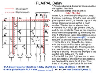
•PLA delay = max(delay from any input literal to an o/p)
•Each literal signal incurs a delay (D 1) that is proportional to the # of
transistors it drives. It is thus important to balance the # of transistors
driven by each literal min(max # of chosen PIs that each literal is in)
•Each PI signal’s delay on the AND line (D 2) is also similarly
proportional to the # of transistors in the OR array that it drives (i.e., on
the # of functions it belongs to). So this delay can be minimized by
min(max # of functions each PI is in). ). However, PI sharing is useful
for cost min. so we ignore this aspect of delay here. (Can we
augment QM to consider extra delay on AND line when PI is shared,
and tradeoff delay w/ cost as we do below for literal lines?)
•But either Rule 6 or Rule 7 followed by the sweep-up phase should be
used to reduce unnecessary sharing, as the latter can increase the PI
signal’s delay.
•Thus for combined h/w & delay (D 1 only) min., start w/ a PI cost = 1
(for h/w cost; this will min # of AND lines). After a PI g is chosen,
increase the cost of each PI h by w if g and h share at least 1 common
literal that currently is in the largest # of chosen PIs so far. Otherwise, f(A,B,C,D) = Σ m(1,3,5,7,9) + Σ d(2,6,12,13)
Ex:
there is no increase in g’s cost.
MSBs
AB
•This is done, since such literals in g will drive an additional transistor
CD
00
01
11
10
gate if g is subsequently chosen, thus increasing the D 1 delay. It is
4
12 x
8
should thus be “expensive” to choose a PI such as g.
00 0
LSBs
•w is the ``norm. weight’’ of the importance of delay compared to
5 1 13 x 9 1
01 1 1
hardware cost (AND lines). E.g., w = 0.2 we can sacrifice delay by
CD
3 1
7 1 15
11
up to (1/0.2)*a = 5α units in order to save 1 AND line, where α <= 1 is
the estimated fraction of the contribution of D 1 to the total PLA/PAL
11
AD
delay. On the other hand, w = 2 we can sacrifice a delay increase of
6 x
14
10
10 2 x
up to (1/2)*a = 0.5α units to save 1 AND line or conversely, we can
AC
sacrifice up to 1 AND line to not incur a delay increase of 0.5α units.
•
cost(C’D) = 1 + 0.2 = cost(A’D) = cost(A’C) (w =
•The covering rule can be applied taking this cost into consideration
0.2)
(e.g., for two PIs that cover each other, delete the higher-cost one, and • C’D is an EPI choose it cost(A’D) incr. to
1.2 + 0.2 (due to common literal D driving max
by not deleting a lower-cost covered PI—either PI-pair based covering
so far)
or least cost/MTs based heur. can be used to break such a “pseudo- • trans. [1] covers = 1.4A’D bad covers A’C
A’C good
A’D,
cyclic” table)
delete A’D A’C is a p-EPI choose A’C
•
Final soln: f = C’D + A’C has a smaller delay in a
PLA than the alternate soln. of C’D + A’D](https://image.slidesharecdn.com/pla-pal-and-pla-optimization-140101120645-phpapp01/85/Pla-pal-and-pla-optimization-12-320.jpg)
![Delay optimization (Initial Cost Formulation): QM for PLA Hardware (H/W) + Delay Opt.
•PLA delay = max(delay from any input literal to an o/p)
•Each literal signal incurs a delay (D 1) that is proportional to the # of
transistors it drives. It is thus important to balance the # of transistors
driven by each literal min(max # of chosen PIs that each literal is in)
•Each PI signal’s delay on the AND line (D 2) is also similarly
proportional to the # of transistors in the OR array that it drives (i.e., on
the # of functions it belongs to). So this delay can be minimized by
min(max # of functions each PI is in). However, PI sharing is useful for
cost min. so we ignore this aspect of delay here. (Can we augment
QM to consider extra delay on AND line when PI is shared, and
tradeoff delay w/ cost as we do below for literal lines?)
•But either Rule 6 or Rule 7 followed by the sweep-up phase should be
used to reduce unnecessary sharing, as the latter can increase the PI
signal’s delay.
•Thus for combined h/w & delay (D 1 only) min., start w/ a PI cost = 1
(for h/w cost; this will min # of AND lines). After a PI g is chosen,
increase the cost of each PI h by w if g and h share at least 1 common
literal that currently is in the largest # of chosen PIs so far. Otherwise, • An alternate cost is to have the cost grow
there is no increase in g’s cost.
slowly as opposed to being binary w/ a sharp
•This is done, since such literals in g will drive an additional transistor step (go from 0 to 1 as soon as a literal goes
gate if g is subsequently chosen, thus increasing the D 1 delay. It is
from being in max-1 to max # of PIs so far).
should thus be “expensive” to choose a PI such as g.
• So when PI g is selected, for every PI h that g
has common literal(s) with, determine among
•w is the ``norm. weight’’ of the importance of delay compared to
hardware cost (AND lines). E.g., w = 0.2 we can sacrifice delay by these literals, the max. # k of chosen PIs they
up to (1/0.2)*a = 5α units in order to save 1 AND line, where α <= 1 is occur in
the estimated fraction of the contribution of D 1 to the total PLA/PAL
• E.g., incr. cost by w*(e/(e-1))*(1-e-(k/kmax) )) OR
delay. On the other hand, w = 2 we can sacrifice a delay increase of w(e-(1-[k/kmax]) )) OR w*k/kmax, where kmax is the
up to (1/2)*a = 0.5α units to save 1 AND line or conversely, we can
globally max. # of chosen PIs that a literal (a
sacrifice up to 1 AND line to not incur a delay increase of 0.5α units.
critical literal) is currently present in.
• This allows us to “anticipate” and consider
•The covering rule can be applied taking this cost into consideration
(e.g., for two PIs that cover each other, delete the higher-cost one, and costs of literals that can get critical in the nearby not deleting a lower-cost covered PI—either PI-pair based covering future in the QM opt. process.
or least cost/MTs based heur. can be used to break such a “pseudo- • But this does not do “look-ahead” (check
cyclic” table)
what PIs are remaining and for each literal
estimate how many it belongs to will be
chosen. What is a good look-ahead estimate?](https://image.slidesharecdn.com/pla-pal-and-pla-optimization-140101120645-phpapp01/85/Pla-pal-and-pla-optimization-13-320.jpg)

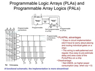
This document discusses programmable logic arrays (PLAs) and programmable array logics (PALs). It describes how PLAs and PALs are implemented using programmable connections and compares their advantages over traditional gate-based designs. The document also discusses optimizations for PLA/PAL hardware cost and delay, including minimizing the number of product terms and balancing the number of transistors driven by each literal to reduce delay. It proposes using a cost function that considers both hardware cost and delay during the optimization process.