PIC MICROCONTROLLER


              By : Osama Hasan
AN INTRODUCTION TO PIC MICROCONTROLLERS

- The name PIC was originally an acronym for "Programmable
Intelligent Computer".

- A PIC microcontroller is a processor with built in memory and
RAM and you can use it to control your projects.

- What this really means for you is that you have a very powerful
device that has many useful built in modules e.g.

* EEPROM.
* Timers.
* Analogue comparators.
* UART.
INTRODUCTION (CONT.)

Why PIC is popular?

   low cost ,wide availability with high clock speed
   availability of low cost or free development tools
   Only 37 instructions to remember
   serial programming and re-programming with flash
    memory capability
   Its code is extremely efficient, allowing the PIC to run
    with typically less program memory than its larger
    competitors
   PIC is very small and easy to implement for non-
    complex problems and usually accompanies to the
    microprocessors as an interface
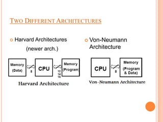
TWO DIFFERENT ARCHITECTURES

   Harvard Architectures    Von-Neumann

        (newer arch.)        Architecture
TWO DIFFERENT ARCHITECTURES

   Harvard Architectures                 Von-Neumann Architecture


   Used mostly in RISC CPUs
                                          Used in: 80X86 (CISC PCs)
   Separate program bus and data
    bus: can be of different widths       Only one bus between CPU and
                                           memory
   For example, PICs use:                RAM and program memory
     Data memory (RAM): a small           share the same bus and the
      number of 8bit registers             same memory, and so must have
     Program memory (ROM):                the same bit width.
      12bit, 14bit or 16bit wide (in
      EPROM, FLASH, or ROM)
RISC VS. CISC
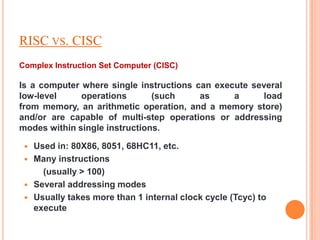
Complex Instruction Set Computer (CISC)

Is a computer where single instructions can execute several
low-level     operations       (such     as     a     load
from memory, an arithmetic operation, and a memory store)
and/or are capable of multi-step operations or addressing
modes within single instructions.

    Used in: 80X86, 8051, 68HC11, etc.
    Many instructions
       (usually > 100)
    Several addressing modes
    Usually takes more than 1 internal clock cycle (Tcyc) to
     execute
RISC VS. CISC
Reduced Instruction Set Computer (RISC)

Is a CPU design strategy based on the insight that simplified
instructions can provide higher performance if this simplicity enables
much faster execution of each instruction. A computer based on this
strategy is a reduced instruction set computer also called RISC.


      Used in: SPARC, ALPHA, Atmel AVR, etc.
      Few instructions
        (usually < 50)
      Only a few addressing modes
      Executes 1 instruction in 1 internal clock cycle (Tcyc)
FAMILY CORE ARCHITECTURE DIFFERENCES

 The     PIC Family: Cores

     12bit cores with 33 instructions: 12C50x, 16C5x

     14bit cores with 35 instructions: 12C67x,16Cxxx

     16bit cores with 58 instructions: 17C4x,17C7xx

     ‘Enhanced’ 16bit cores with 77 instructions: 18Cxxx
THE PIC FAMILY: SPEED
 Can use crystals, clock oscillators, or even an RC circuit.
 Some PICs have a built in 4MHz RC clock, Not very
  accurate, but requires no external components!
 Instruction speed = 1/4 clock speed (Tcyc = 4 * Tclk)
 All PICs can be run from DC to their maximum specified
  speed:
                      12C50x            4MHz


                      12C67x            10MHz
                      16Cxxx            20MHz
                      17C4x / 17C7xxx   33MHz
                      18Cxxx            40MHz
CLOCK AND INSTRUCTION CYCLES
 Instruction     Clock
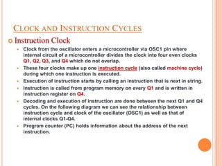
     Clock from the oscillator enters a microcontroller via OSC1 pin where
      internal circuit of a microcontroller divides the clock into four even clocks
      Q1, Q2, Q3, and Q4 which do not overlap.
     These four clocks make up one instruction cycle (also called machine cycle)
      during which one instruction is executed.
     Execution of instruction starts by calling an instruction that is next in string.
     Instruction is called from program memory on every Q1 and is written in
      instruction register on Q4.
     Decoding and execution of instruction are done between the next Q1 and Q4
      cycles. On the following diagram we can see the relationship between
      instruction cycle and clock of the oscillator (OSC1) as well as that of
      internal clocks Q1-Q4.
     Program counter (PC) holds information about the address of the next
      instruction.
CLOCK AND INSTRUCTION CYCLES (CONT.)
PIPELINING IN PIC
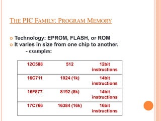
THE PIC FAMILY: PROGRAM MEMORY

 Technology: EPROM, FLASH, or ROM
 It varies in size from one chip to another.
       - examples:

       12C508          512            12bit
                                  instructions
       16C711       1024 (1k)         14bit
                                  instructions
       16F877       8192 (8k)         14bit
                                  instructions
       17C766      16384 (16k)        16bit
                                  instructions
MICROCHIP PIC 16F84 MICROCONTROLLER

High Performance RISC CPU:

Only 35 single word instructions to learn

All single cycle instructions except for program
branches, which are two-cycle

Operating speed: DC - 20 MHz clock input DC - 200
ns instruction cycle
MICROCHIP PIC 16F84 MICROCONTROLLER

Below is a diagram showing the pin-outs of the PIC 16F84. We will
go through each pin, explaining what each is used for.
MICROCHIP PIC 16F84 MICROCONTROLLER

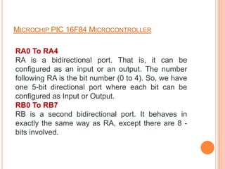
RA0 To RA4
RA is a bidirectional port. That is, it can be
configured as an input or an output. The number
following RA is the bit number (0 to 4). So, we have
one 5-bit directional port where each bit can be
configured as Input or Output.
RB0 To RB7
RB is a second bidirectional port. It behaves in
exactly the same way as RA, except there are 8 -
bits involved.
MICROCHIP PIC 16F84 MICROCONTROLLER

VSS And VDD
These are the power supply pins. VDD is the
positive supply, and VSS is the negative
supply, or 0V. The maximum supply voltage that
you can use is 6V, and the minimum is 2V.

OSC1/CLK IN And OSC2/CLKOUT
These pins is where we connect an external
clock, so that the microcontroller has some kind
of timing.
MICROCHIP PIC 16F84 MICROCONTROLLER

MCLR
This pin is used to erase the memory locations
inside the PIC (i.e. when we want to re-program
it. In normal use it is connected to the positive
supply rail.

T0CK1
This is another clock input, which operates an
internal timer. It operates in isolation to the main
clock.
MICROCHIP PIC 16F84 MICROCONTROLLER

Below is a diagram showing the pin-outs of the PIC 16F84. We will
go through each pin, explaining what each is used for.


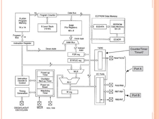
 PORT A


PORT B
PIC DATA MEMORY
The most
important
registers
have
addresses
in all the
four
banks


             The data memory is devided into 4 memory banks
THE REGISTERS
A register is a place inside the PIC that can be written to, read from
or both.

you will notice is that it is split into two - Bank 0 and Bank
1. Bank 1 is used to control the actual operation of the PIC, for
example to tell the PIC which bits of Port A are input and which
are output. Bank 0 is used to manipulate the data.


An example is as follows: Let us say we want to make one bit on
Port A high. First we need to go to Bank 1 to set the particular
bit, or pin, on Port A as an output. We then come back to Bank 0
and send a logic 1 (bit 1) to that pin.
THE REGISTERS

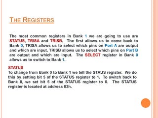
The most common registers in Bank 1 we are going to use are
STATUS, TRISA and TRISB. The first allows us to come back to
Bank 0, TRISA allows us to select which pins on Port A are output
and which are input, TRISB allows us to select which pins on Port B
are output and which are input. The SELECT register in Bank 0
allows us to switch to Bank 1.

STATUS
To change from Bank 0 to Bank 1 we tell the STAUS register. We do
this by setting bit 5 of the STATUS register to 1. To switch back to
Bank 0, we set bit 5 of the STATUS register to 0. The STATUS
register is located at address 03h.
THE REGISTERS

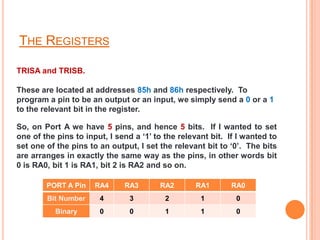
TRISA and TRISB.

These are located at addresses 85h and 86h respectively. To
program a pin to be an output or an input, we simply send a 0 or a 1
to the relevant bit in the register.

So, on Port A we have 5 pins, and hence 5 bits. If I wanted to set
one of the pins to input, I send a ‘1’ to the relevant bit. If I wanted to
set one of the pins to an output, I set the relevant bit to ‘0’. The bits
are arranges in exactly the same way as the pins, in other words bit
0 is RA0, bit 1 is RA1, bit 2 is RA2 and so on.

        PORT A Pin    RA4     RA3       RA2       RA1        RA0
        Bit Number     4        3         2         1         0
           Binary      0        0         1         1         0
THE REGISTERS
W ( working register )

The W register is a general register in which you can put any
value that you wish. Once you have assigned a value to W, you
can add it to another value, or move it. If you assign another
value to W, its contents are overwritten.
THE REGISTERS

Now what he have to do is turn an LED on. We do this by
making one of the pins (the one with the LED connected to it)
high. In other words, we send a ‘1’ to the pin.

movlw          02h
movwf          05h

So, now our LED is on, we now need to turn it off:

movlw          00h
movwf          05h
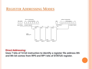
REGISTER ADDRESSING MODES


Direct Addressing:
Uses 7 bits of 14 bit instruction to identify a register file address 8th
and 9th bit comes from RP0 and RP1 bits of STATUS register.
PIC PERIPHERALS

The PIC microcontroller has many built
in peripherals and this can make using them
quite daunting at first which is why I have made
this introductory page with a summary of each
major peripheral block.
PIC PERIPHERALS

      PIC microcontroller     PIC microcontroller
           Feature            feature description
        Flash memory           Re-programmable
                               program storage.
             RAM              Memory storage for
                                 variables.
           EEPROM           Long term stable memory
                              : Electrically Erasable
                               Programmable Read
                                   Only Memory.
           I/O ports        High current Input/output
                                 ports (with pin
                               direction change).
           USART             Built in RS232 protocol
                                (only needs level
                                 translator chip).
PIC PERIPHERALS

Flash memory
This is the program storage area and gives you the most
important benefit for using a PIC microcontroller - You program
the device many times.


 PIC microcontroller RAM
 The PIC microcontroller RAM size is also important as it stores
 all your variables and intermediate data.

 Note: You can usually alter the program to use less RAM by
 choosing the right variable sizes or changing how your program
 works

 For example don't use floating point alter it to use a different
 variable type e.g. you can use long integers with fixed point
 operation to avoid floating point.
PIC PERIPHERALS

PIC microcontroller EEROM

Electrically Erasable ROM is used to store data that must be
saved between power up and power down.

This area is readable and writable and has a much longer life
than the main program store i.e. it has been designed for more
frequent use.
PIC PERIPHERALS

I/O Ports
Input / Output ports let you communicate with the outside world so
you can control leds, LCDs or just about anything with the right
interface. You can also set them as inputs to gather information.

Pin direction
Most PIC microcontroller pins can be set as an input or and output
and this can be done on the fly e.g. for a dallas 1 wire system a pin
can be written to generate data and read at a later stage. The TRIS
register controls the I/O direction and setting a bit in this register
to zero sets the pin as output while setting it as one sets the pin
as input.
Thanks for Attendance

PIC introduction + mapping

  • 1.
    PIC MICROCONTROLLER By : Osama Hasan
  • 2.
    AN INTRODUCTION TOPIC MICROCONTROLLERS - The name PIC was originally an acronym for "Programmable Intelligent Computer". - A PIC microcontroller is a processor with built in memory and RAM and you can use it to control your projects. - What this really means for you is that you have a very powerful device that has many useful built in modules e.g. * EEPROM. * Timers. * Analogue comparators. * UART.
  • 3.
    INTRODUCTION (CONT.) Why PICis popular?  low cost ,wide availability with high clock speed  availability of low cost or free development tools  Only 37 instructions to remember  serial programming and re-programming with flash memory capability  Its code is extremely efficient, allowing the PIC to run with typically less program memory than its larger competitors  PIC is very small and easy to implement for non- complex problems and usually accompanies to the microprocessors as an interface
  • 4.
    TWO DIFFERENT ARCHITECTURES  Harvard Architectures  Von-Neumann (newer arch.) Architecture
  • 5.
    TWO DIFFERENT ARCHITECTURES  Harvard Architectures  Von-Neumann Architecture  Used mostly in RISC CPUs  Used in: 80X86 (CISC PCs)  Separate program bus and data bus: can be of different widths  Only one bus between CPU and memory  For example, PICs use:  RAM and program memory  Data memory (RAM): a small share the same bus and the number of 8bit registers same memory, and so must have  Program memory (ROM): the same bit width. 12bit, 14bit or 16bit wide (in EPROM, FLASH, or ROM)
  • 6.
    RISC VS. CISC ComplexInstruction Set Computer (CISC) Is a computer where single instructions can execute several low-level operations (such as a load from memory, an arithmetic operation, and a memory store) and/or are capable of multi-step operations or addressing modes within single instructions.  Used in: 80X86, 8051, 68HC11, etc.  Many instructions (usually > 100)  Several addressing modes  Usually takes more than 1 internal clock cycle (Tcyc) to execute
  • 7.
    RISC VS. CISC ReducedInstruction Set Computer (RISC) Is a CPU design strategy based on the insight that simplified instructions can provide higher performance if this simplicity enables much faster execution of each instruction. A computer based on this strategy is a reduced instruction set computer also called RISC.  Used in: SPARC, ALPHA, Atmel AVR, etc.  Few instructions (usually < 50)  Only a few addressing modes  Executes 1 instruction in 1 internal clock cycle (Tcyc)
  • 8.
    FAMILY CORE ARCHITECTUREDIFFERENCES  The PIC Family: Cores  12bit cores with 33 instructions: 12C50x, 16C5x  14bit cores with 35 instructions: 12C67x,16Cxxx  16bit cores with 58 instructions: 17C4x,17C7xx  ‘Enhanced’ 16bit cores with 77 instructions: 18Cxxx
  • 9.
    THE PIC FAMILY:SPEED  Can use crystals, clock oscillators, or even an RC circuit.  Some PICs have a built in 4MHz RC clock, Not very accurate, but requires no external components!  Instruction speed = 1/4 clock speed (Tcyc = 4 * Tclk)  All PICs can be run from DC to their maximum specified speed: 12C50x 4MHz 12C67x 10MHz 16Cxxx 20MHz 17C4x / 17C7xxx 33MHz 18Cxxx 40MHz
  • 10.
    CLOCK AND INSTRUCTIONCYCLES  Instruction Clock  Clock from the oscillator enters a microcontroller via OSC1 pin where internal circuit of a microcontroller divides the clock into four even clocks Q1, Q2, Q3, and Q4 which do not overlap.  These four clocks make up one instruction cycle (also called machine cycle) during which one instruction is executed.  Execution of instruction starts by calling an instruction that is next in string.  Instruction is called from program memory on every Q1 and is written in instruction register on Q4.  Decoding and execution of instruction are done between the next Q1 and Q4 cycles. On the following diagram we can see the relationship between instruction cycle and clock of the oscillator (OSC1) as well as that of internal clocks Q1-Q4.  Program counter (PC) holds information about the address of the next instruction.
  • 11.
    CLOCK AND INSTRUCTIONCYCLES (CONT.)
  • 12.
  • 13.
    THE PIC FAMILY:PROGRAM MEMORY  Technology: EPROM, FLASH, or ROM  It varies in size from one chip to another. - examples: 12C508 512 12bit instructions 16C711 1024 (1k) 14bit instructions 16F877 8192 (8k) 14bit instructions 17C766 16384 (16k) 16bit instructions
  • 14.
    MICROCHIP PIC 16F84MICROCONTROLLER High Performance RISC CPU: Only 35 single word instructions to learn All single cycle instructions except for program branches, which are two-cycle Operating speed: DC - 20 MHz clock input DC - 200 ns instruction cycle
  • 15.
    MICROCHIP PIC 16F84MICROCONTROLLER Below is a diagram showing the pin-outs of the PIC 16F84. We will go through each pin, explaining what each is used for.
  • 16.
    MICROCHIP PIC 16F84MICROCONTROLLER RA0 To RA4 RA is a bidirectional port. That is, it can be configured as an input or an output. The number following RA is the bit number (0 to 4). So, we have one 5-bit directional port where each bit can be configured as Input or Output. RB0 To RB7 RB is a second bidirectional port. It behaves in exactly the same way as RA, except there are 8 - bits involved.
  • 17.
    MICROCHIP PIC 16F84MICROCONTROLLER VSS And VDD These are the power supply pins. VDD is the positive supply, and VSS is the negative supply, or 0V. The maximum supply voltage that you can use is 6V, and the minimum is 2V. OSC1/CLK IN And OSC2/CLKOUT These pins is where we connect an external clock, so that the microcontroller has some kind of timing.
  • 18.
    MICROCHIP PIC 16F84MICROCONTROLLER MCLR This pin is used to erase the memory locations inside the PIC (i.e. when we want to re-program it. In normal use it is connected to the positive supply rail. T0CK1 This is another clock input, which operates an internal timer. It operates in isolation to the main clock.
  • 19.
    MICROCHIP PIC 16F84MICROCONTROLLER Below is a diagram showing the pin-outs of the PIC 16F84. We will go through each pin, explaining what each is used for. PORT A PORT B
  • 20.
    PIC DATA MEMORY Themost important registers have addresses in all the four banks The data memory is devided into 4 memory banks
  • 21.
    THE REGISTERS A registeris a place inside the PIC that can be written to, read from or both. you will notice is that it is split into two - Bank 0 and Bank 1. Bank 1 is used to control the actual operation of the PIC, for example to tell the PIC which bits of Port A are input and which are output. Bank 0 is used to manipulate the data. An example is as follows: Let us say we want to make one bit on Port A high. First we need to go to Bank 1 to set the particular bit, or pin, on Port A as an output. We then come back to Bank 0 and send a logic 1 (bit 1) to that pin.
  • 23.
    THE REGISTERS The mostcommon registers in Bank 1 we are going to use are STATUS, TRISA and TRISB. The first allows us to come back to Bank 0, TRISA allows us to select which pins on Port A are output and which are input, TRISB allows us to select which pins on Port B are output and which are input. The SELECT register in Bank 0 allows us to switch to Bank 1. STATUS To change from Bank 0 to Bank 1 we tell the STAUS register. We do this by setting bit 5 of the STATUS register to 1. To switch back to Bank 0, we set bit 5 of the STATUS register to 0. The STATUS register is located at address 03h.
  • 24.
    THE REGISTERS TRISA andTRISB. These are located at addresses 85h and 86h respectively. To program a pin to be an output or an input, we simply send a 0 or a 1 to the relevant bit in the register. So, on Port A we have 5 pins, and hence 5 bits. If I wanted to set one of the pins to input, I send a ‘1’ to the relevant bit. If I wanted to set one of the pins to an output, I set the relevant bit to ‘0’. The bits are arranges in exactly the same way as the pins, in other words bit 0 is RA0, bit 1 is RA1, bit 2 is RA2 and so on. PORT A Pin RA4 RA3 RA2 RA1 RA0 Bit Number 4 3 2 1 0 Binary 0 0 1 1 0
  • 25.
    THE REGISTERS W (working register ) The W register is a general register in which you can put any value that you wish. Once you have assigned a value to W, you can add it to another value, or move it. If you assign another value to W, its contents are overwritten.
  • 27.
    THE REGISTERS Now whathe have to do is turn an LED on. We do this by making one of the pins (the one with the LED connected to it) high. In other words, we send a ‘1’ to the pin. movlw 02h movwf 05h So, now our LED is on, we now need to turn it off: movlw 00h movwf 05h
  • 28.
    REGISTER ADDRESSING MODES DirectAddressing: Uses 7 bits of 14 bit instruction to identify a register file address 8th and 9th bit comes from RP0 and RP1 bits of STATUS register.
  • 29.
    PIC PERIPHERALS The PICmicrocontroller has many built in peripherals and this can make using them quite daunting at first which is why I have made this introductory page with a summary of each major peripheral block.
  • 30.
    PIC PERIPHERALS PIC microcontroller PIC microcontroller Feature feature description Flash memory Re-programmable program storage. RAM Memory storage for variables. EEPROM Long term stable memory : Electrically Erasable Programmable Read Only Memory. I/O ports High current Input/output ports (with pin direction change). USART Built in RS232 protocol (only needs level translator chip).
  • 31.
    PIC PERIPHERALS Flash memory Thisis the program storage area and gives you the most important benefit for using a PIC microcontroller - You program the device many times. PIC microcontroller RAM The PIC microcontroller RAM size is also important as it stores all your variables and intermediate data. Note: You can usually alter the program to use less RAM by choosing the right variable sizes or changing how your program works For example don't use floating point alter it to use a different variable type e.g. you can use long integers with fixed point operation to avoid floating point.
  • 32.
    PIC PERIPHERALS PIC microcontrollerEEROM Electrically Erasable ROM is used to store data that must be saved between power up and power down. This area is readable and writable and has a much longer life than the main program store i.e. it has been designed for more frequent use.
  • 33.
    PIC PERIPHERALS I/O Ports Input/ Output ports let you communicate with the outside world so you can control leds, LCDs or just about anything with the right interface. You can also set them as inputs to gather information. Pin direction Most PIC microcontroller pins can be set as an input or and output and this can be done on the fly e.g. for a dallas 1 wire system a pin can be written to generate data and read at a later stage. The TRIS register controls the I/O direction and setting a bit in this register to zero sets the pin as output while setting it as one sets the pin as input.
  • 34.