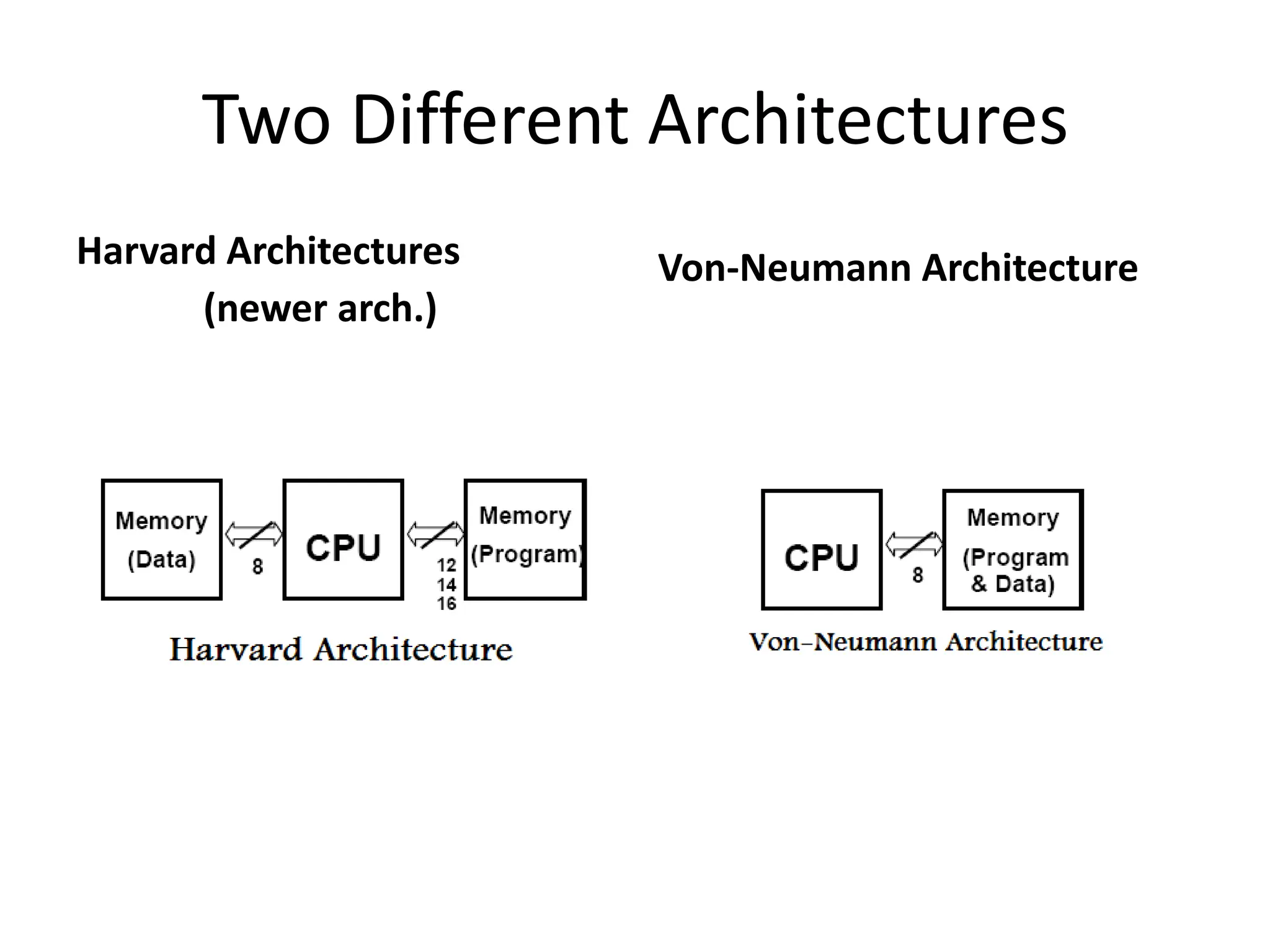
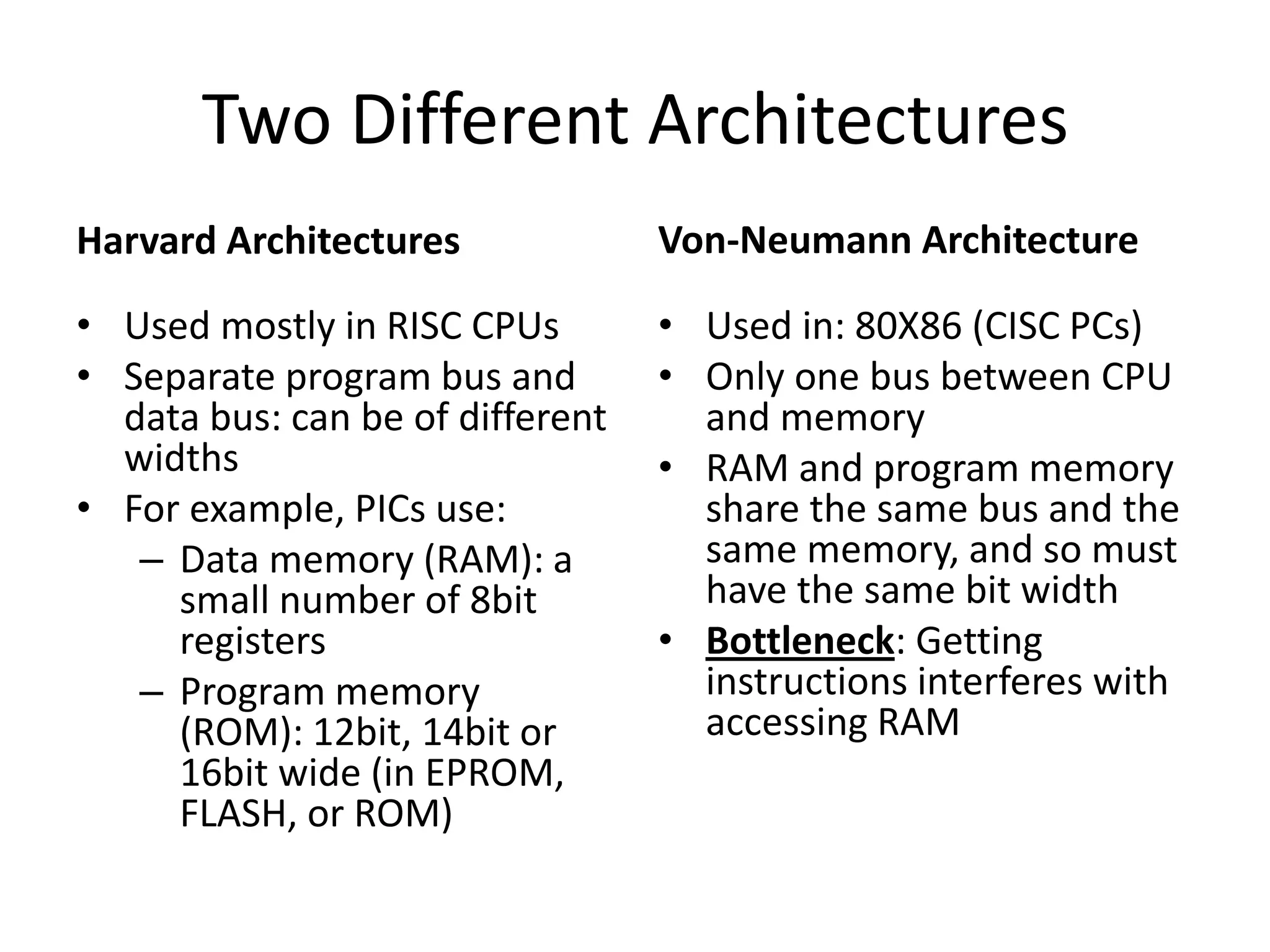
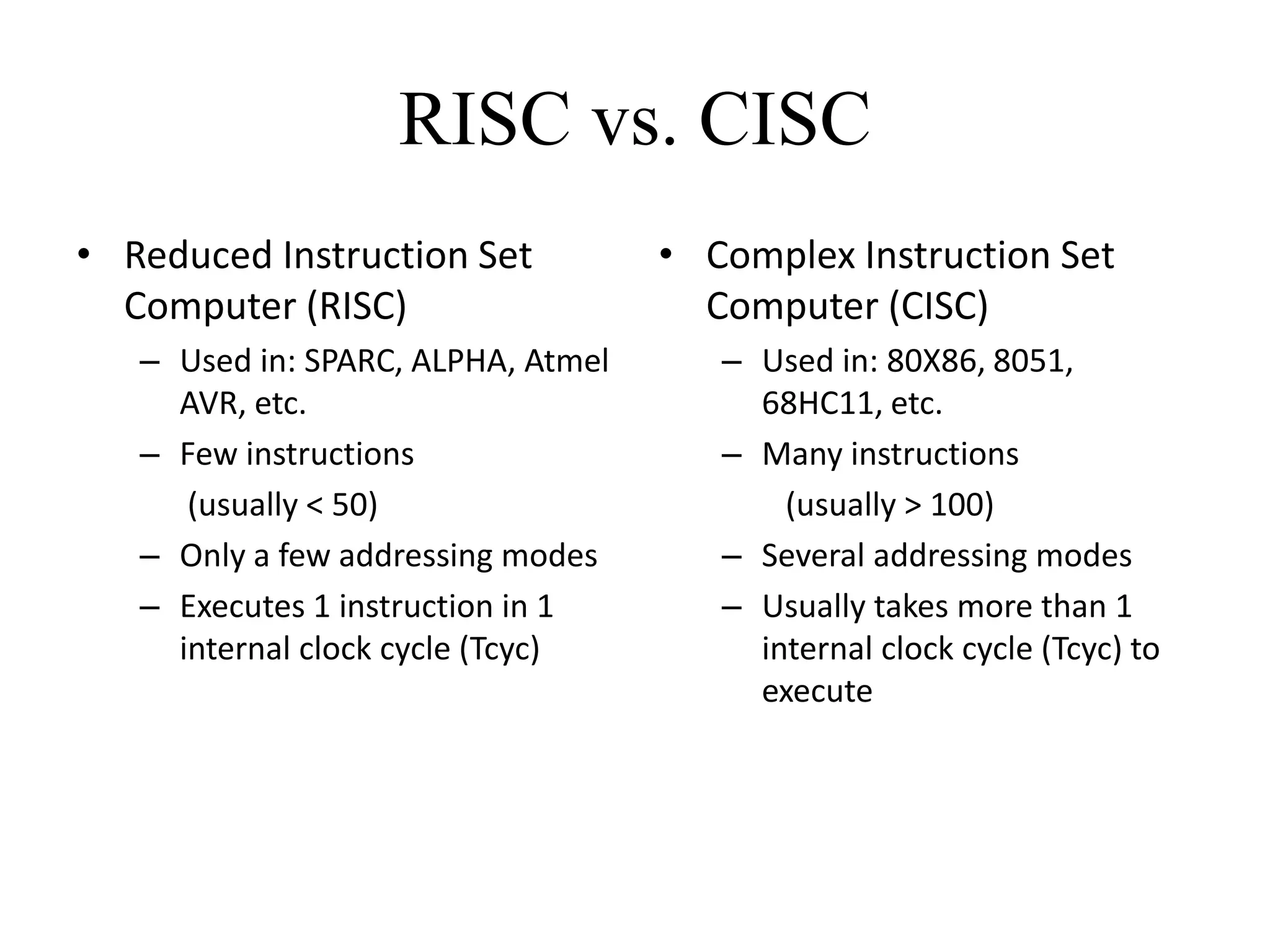
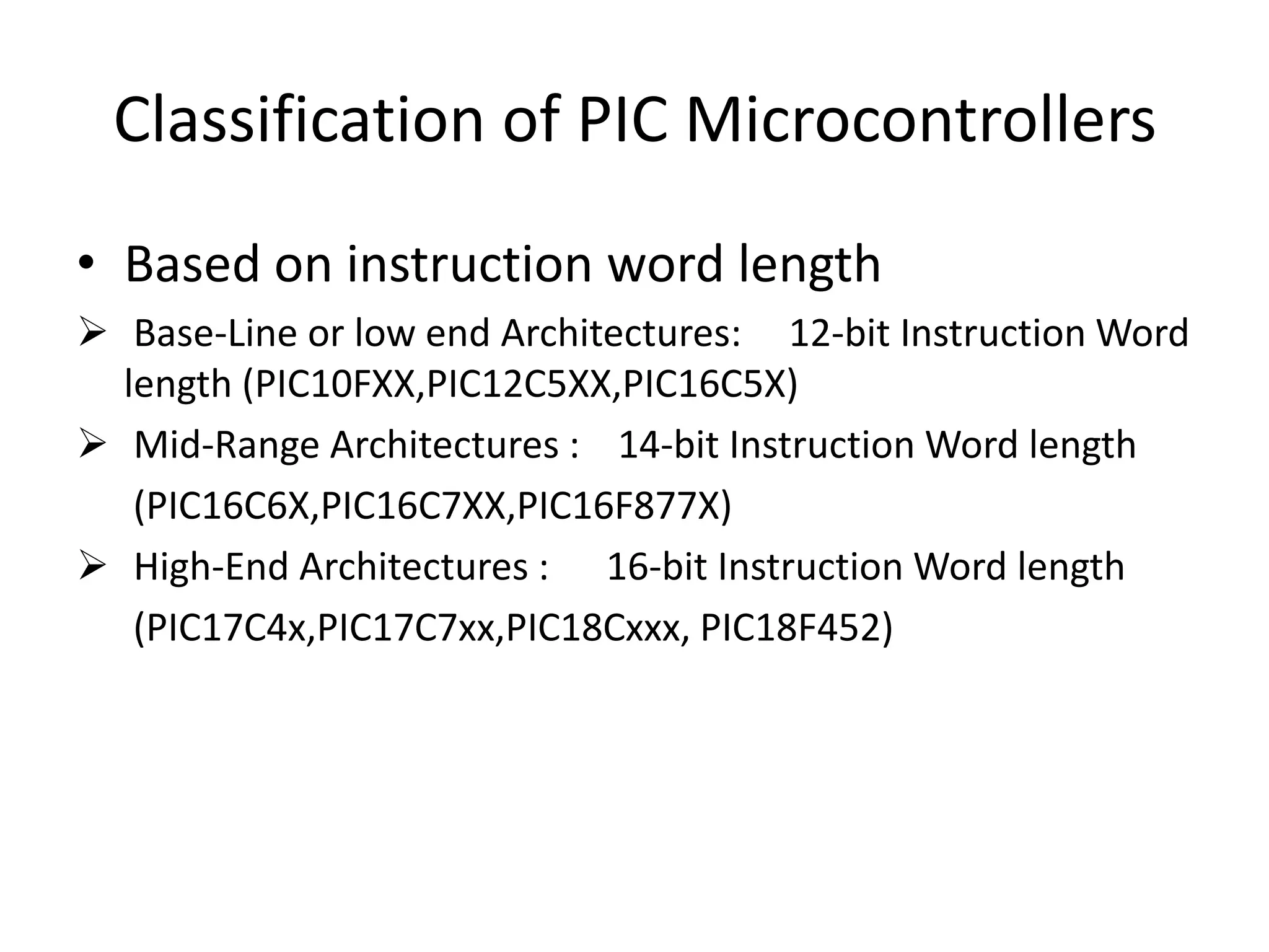
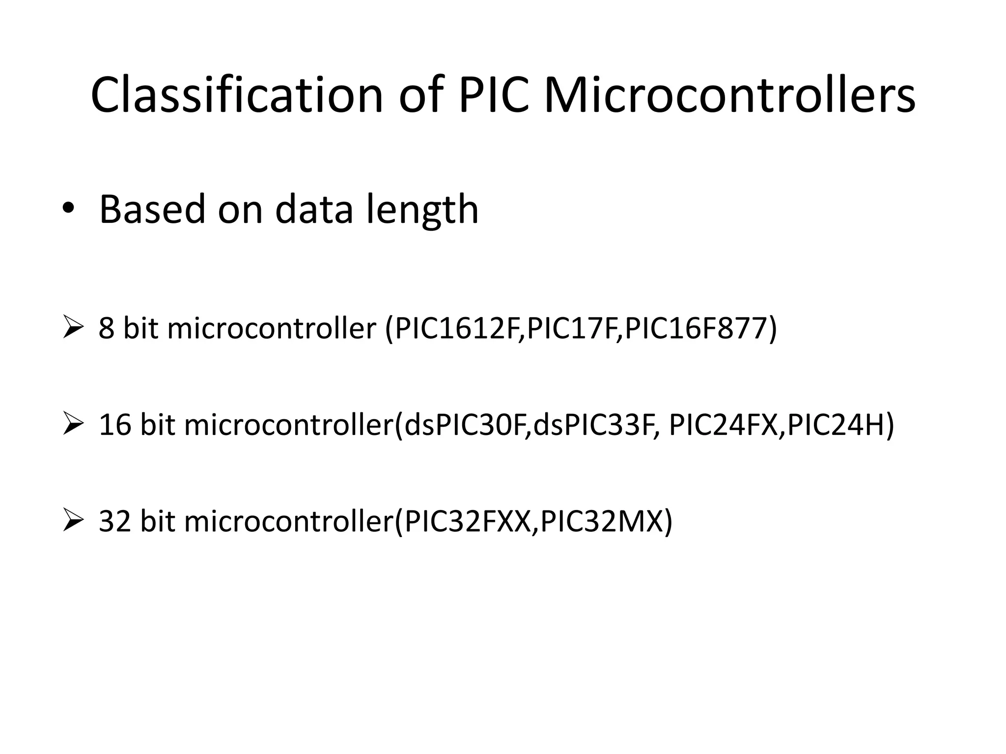
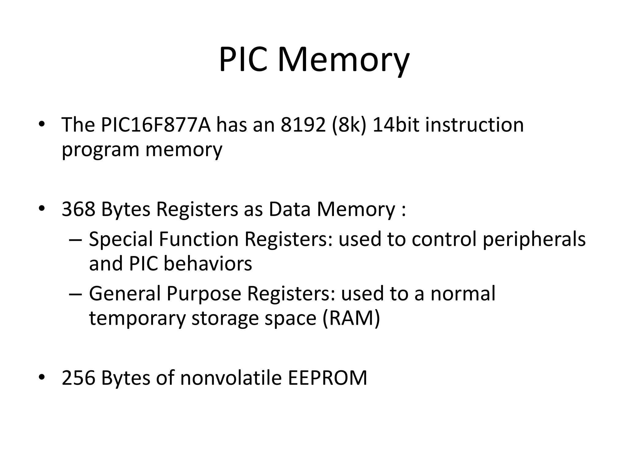
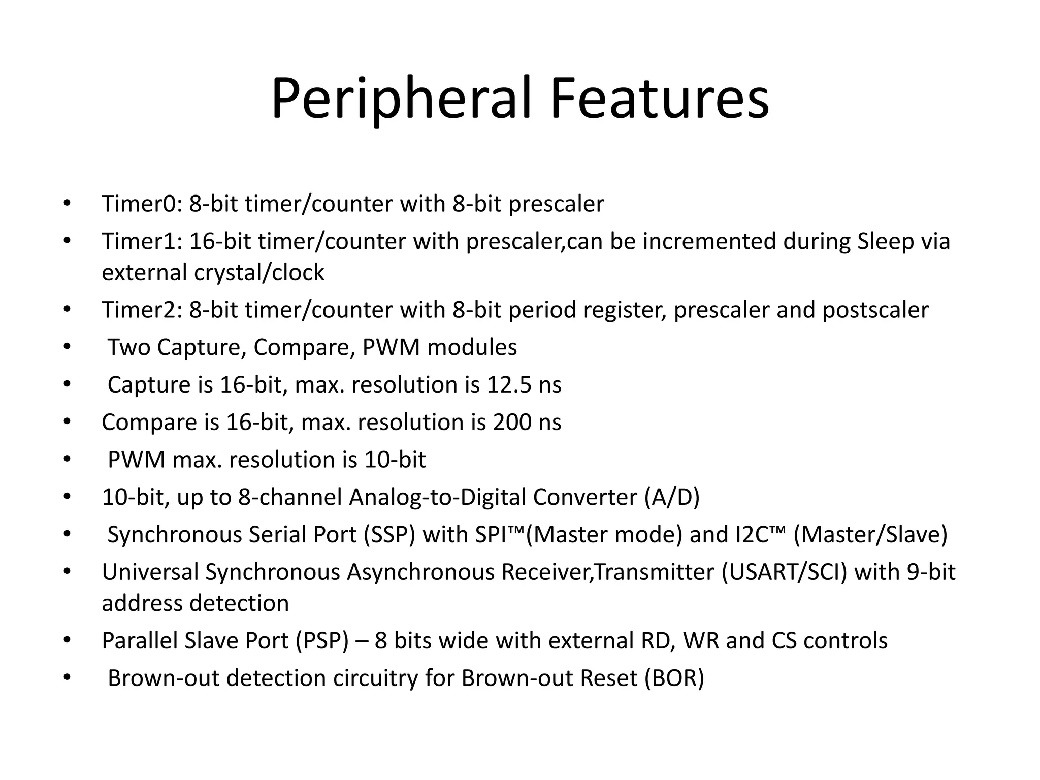
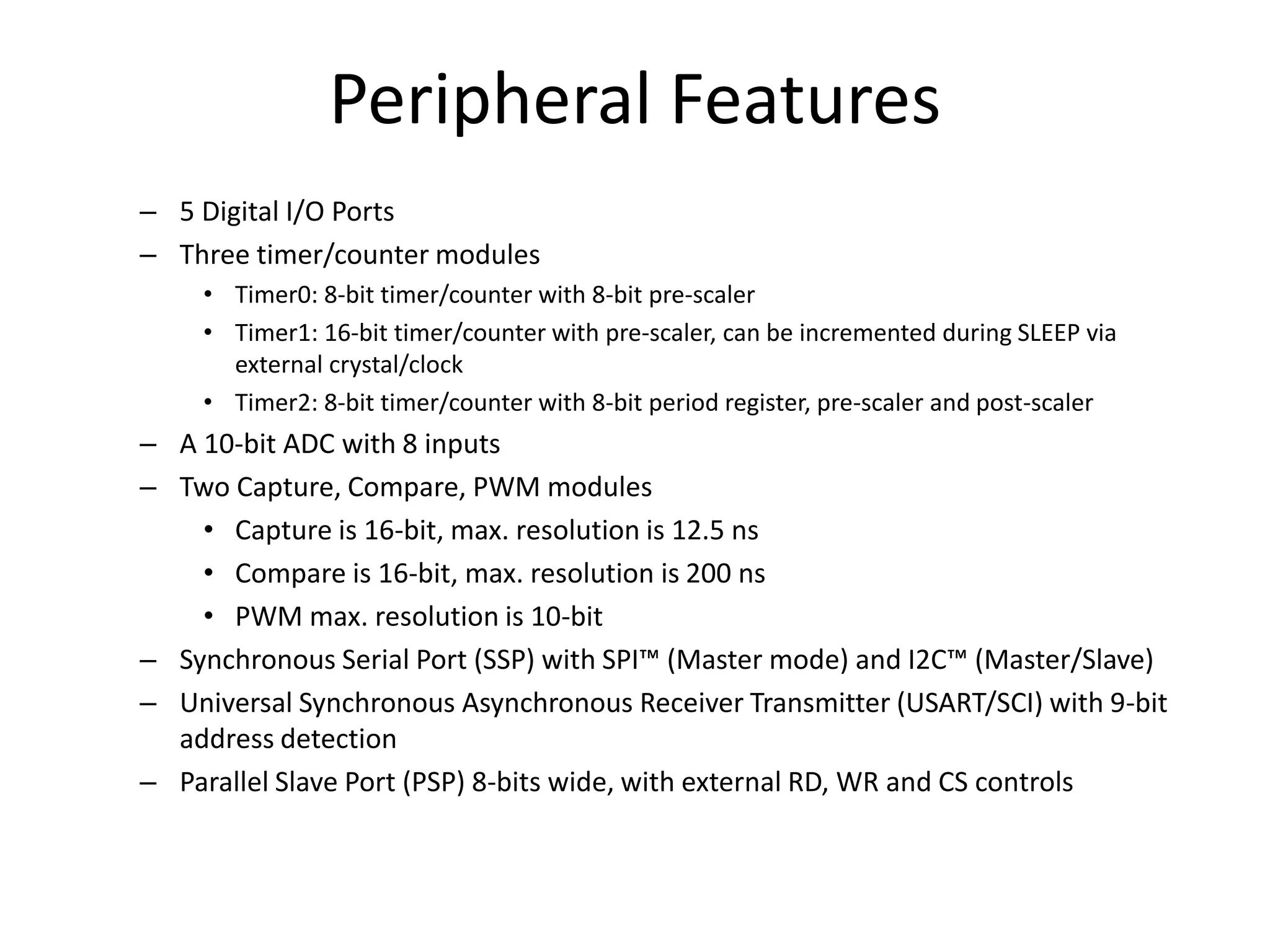
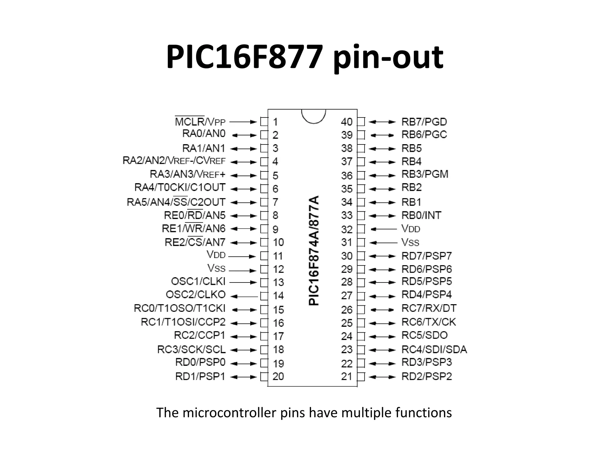
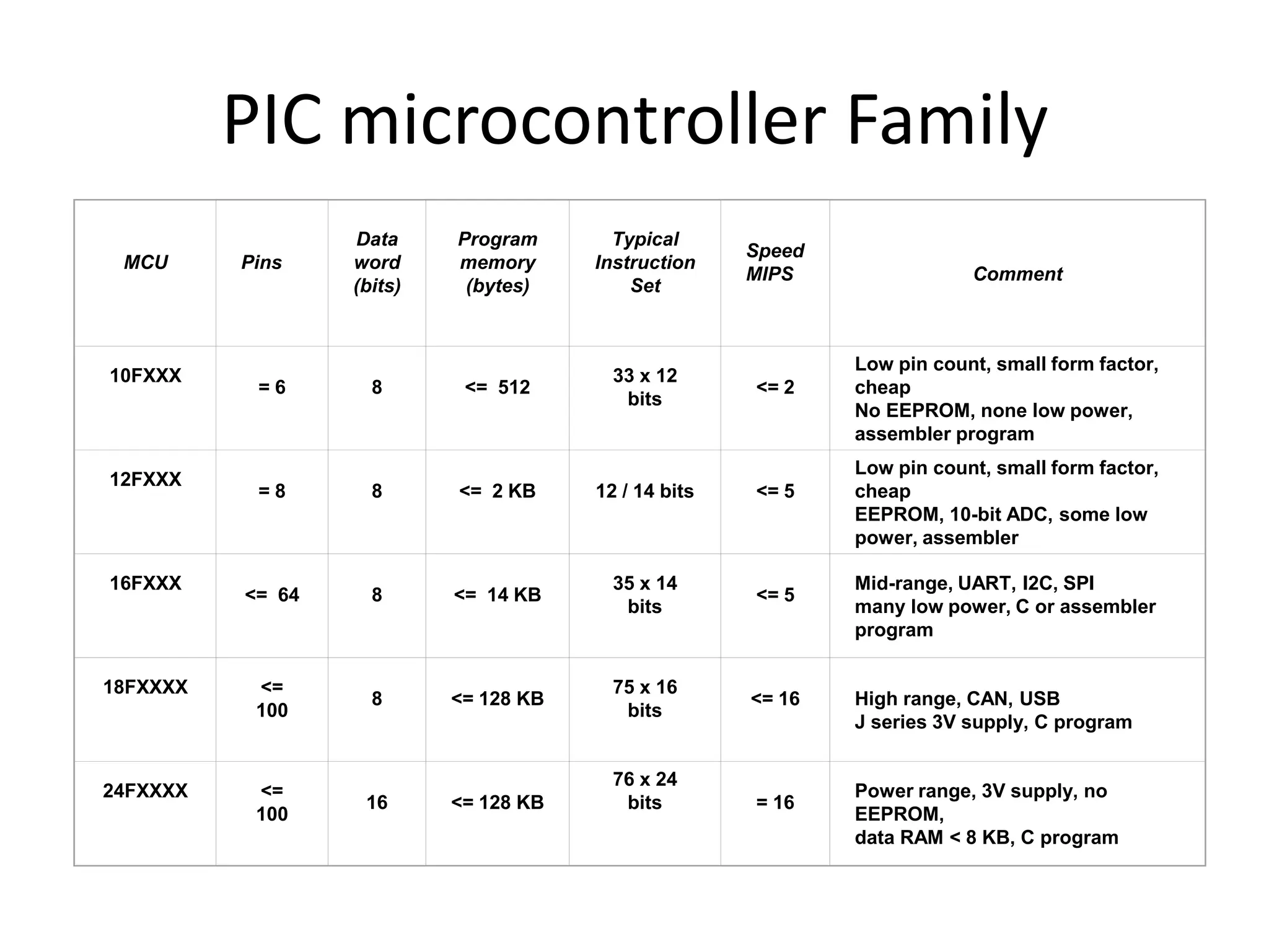
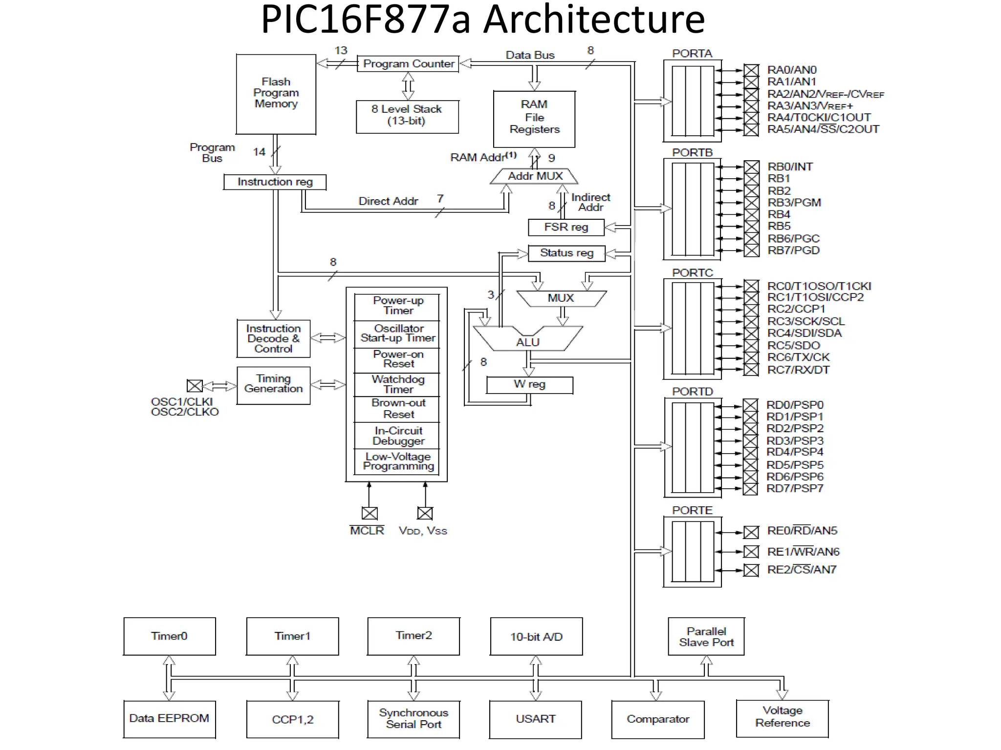
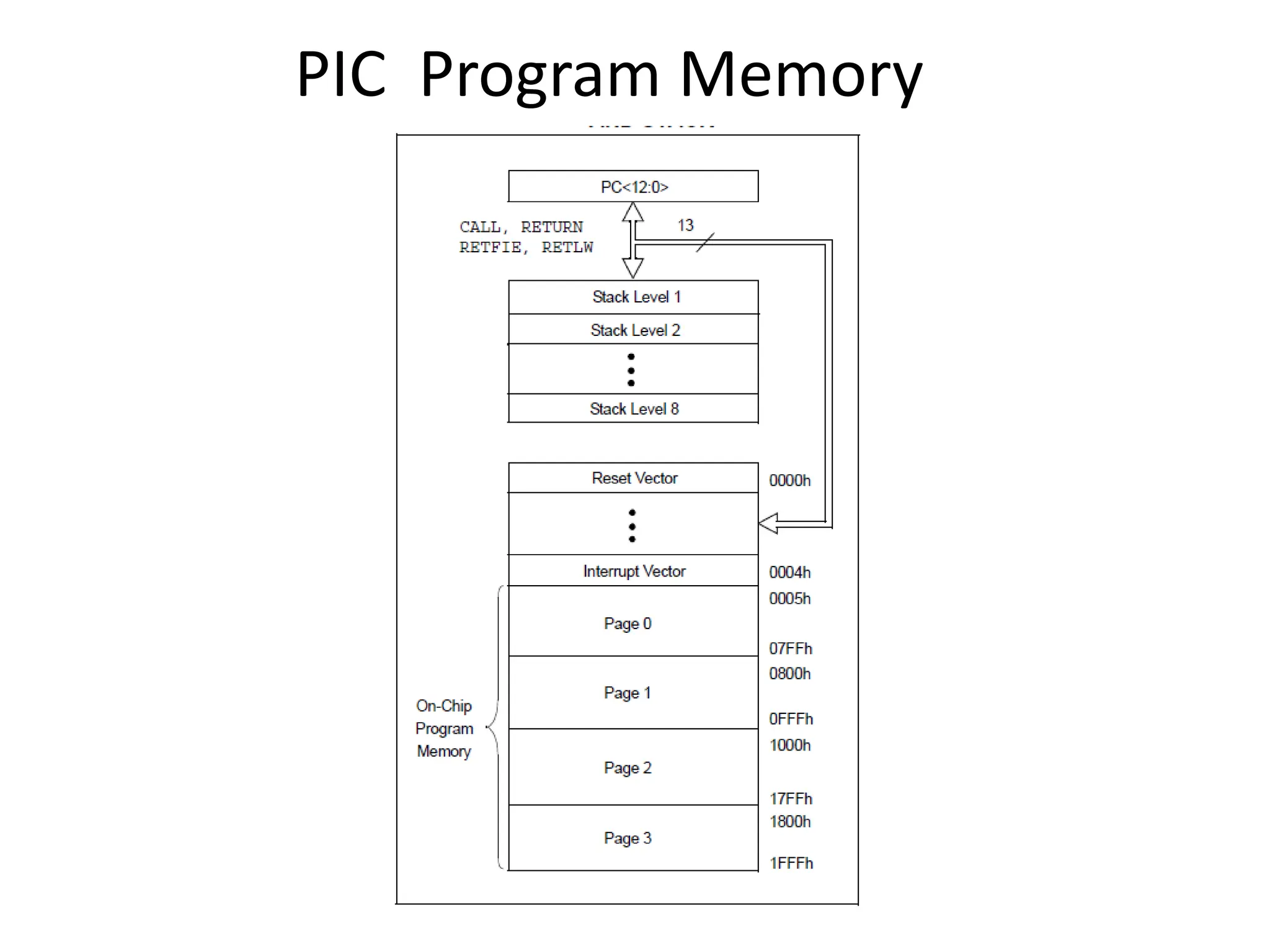
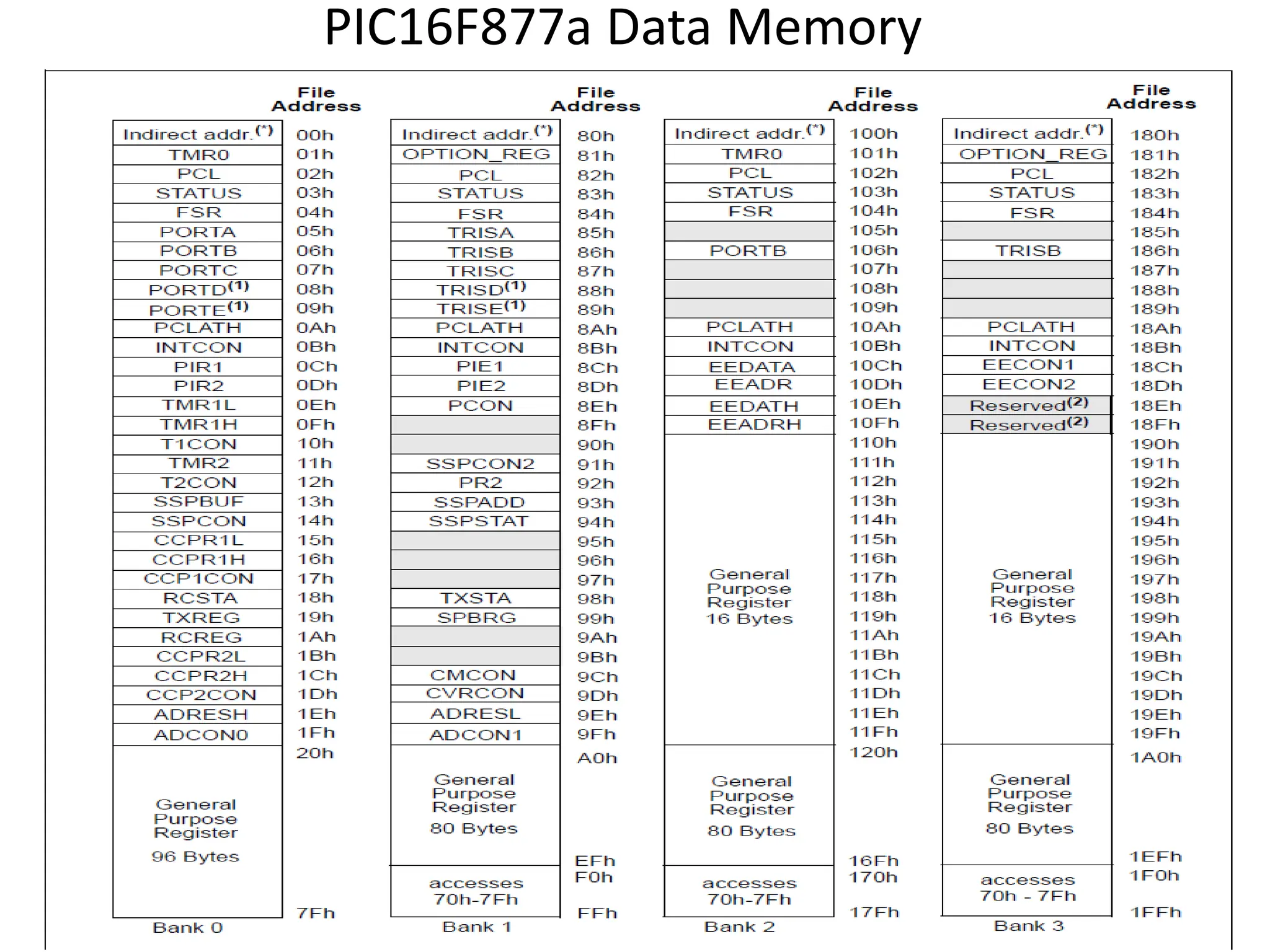
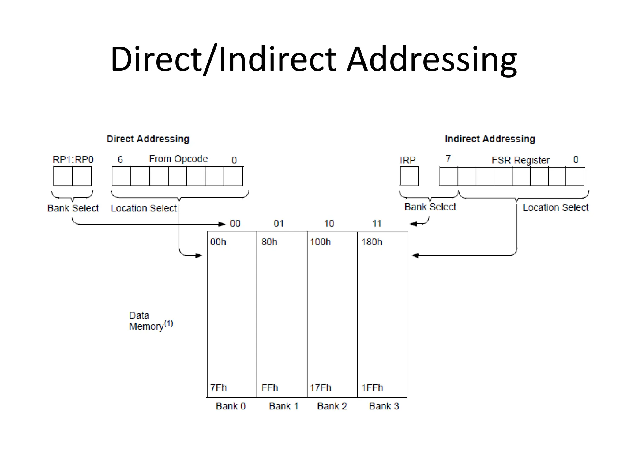
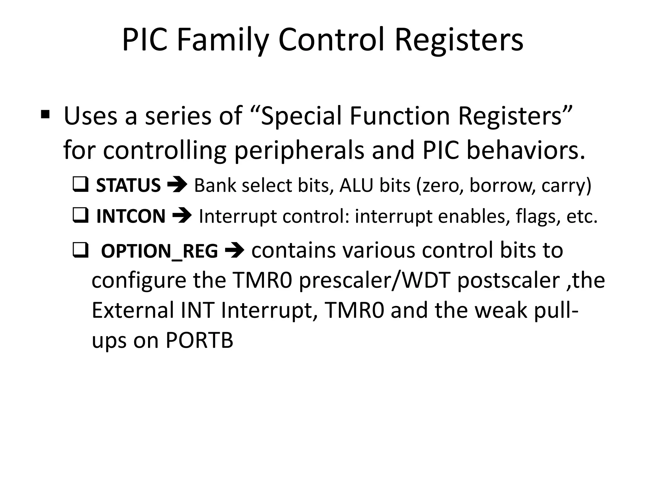
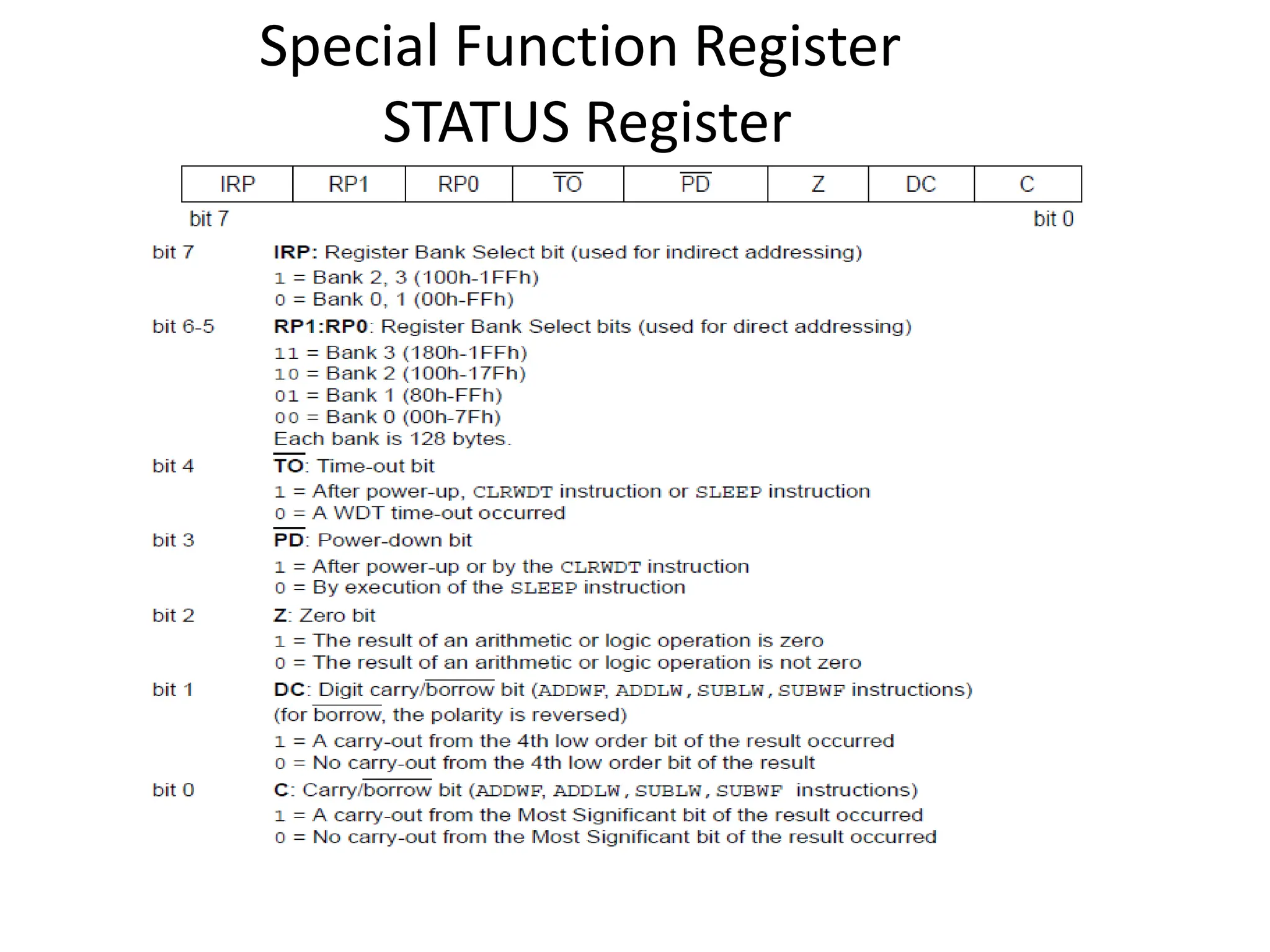
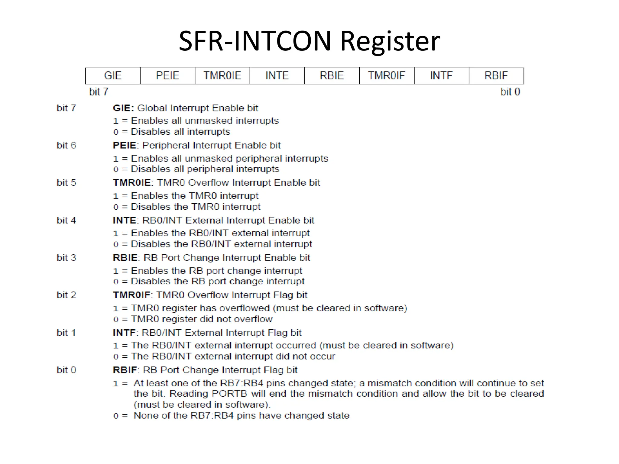
PIC Microcontrollers
PIC16F877a
A.Suyampulingam
Assistant Professor(Sr.Gr)
Introduction
 What is PIC?
• A family of Harvard architecture microcontrollers made by
Microchip Technology.
• Micro Controller : Micro Processor + Peripherals
• Derived from the PIC1650 originally developed by General
Instrument Microelectronics Division.
• The name PIC was originally an acronym for "Programmable
Intelligent Computer".
• The name PIC is referred to Peripheral Interface Controller.
• It shares some common features with RISC designs.
Introduction
 Why PIC is popular?
 low cost ,wide availability with high clock speed
 of low cost or free development tools
 Only 35 instructions to remember
 serial programming and re-programming with flash
memory capability
 Its code is extremely efficient, allowing the PIC to run
with typically less program memory than its larger
competitors
PIC is very small and easy to implement for non-complex
problems and usually accompanies to the microprocessors
as an interface
Two Different Architectures
Harvard Architectures
(newer arch.)
Von-Neumann Architecture
Two Different Architectures
Harvard Architectures
• Used mostly in RISC CPUs
• Separate program bus and
data bus: can be of different
widths
• For example, PICs use:
– Data memory (RAM): a
small number of 8bit
registers
– Program memory
(ROM): 12bit, 14bit or
16bit wide (in EPROM,
FLASH, or ROM)
Von-Neumann Architecture
• Used in: 80X86 (CISC PCs)
• Only one bus between CPU
and memory
• RAM and program memory
share the same bus and the
same memory, and so must
have the same bit width
• Bottleneck: Getting
instructions interferes with
accessing RAM
RISC vs. CISC
• Reduced Instruction Set
Computer (RISC)
– Used in: SPARC, ALPHA, Atmel
AVR, etc.
– Few instructions
(usually < 50)
– Only a few addressing modes
– Executes 1 instruction in 1
internal clock cycle (Tcyc)
• Complex Instruction Set
Computer (CISC)
– Used in: 80X86, 8051,
68HC11, etc.
– Many instructions
(usually > 100)
– Several addressing modes
– Usually takes more than 1
internal clock cycle (Tcyc) to
execute
Classification of PIC Microcontrollers
• Based on instruction word length
 Base-Line or low end Architectures: 12-bit Instruction Word
length (PIC10FXX,PIC12C5XX,PIC16C5X)
 Mid-Range Architectures : 14-bit Instruction Word length
(PIC16C6X,PIC16C7XX,PIC16F877X)
 High-End Architectures : 16-bit Instruction Word length
(PIC17C4x,PIC17C7xx,PIC18Cxxx, PIC18F452)
Classification of PIC Microcontrollers
• Based on data length
 8 bit microcontroller (PIC1612F,PIC17F,PIC16F877)
 16 bit microcontroller(dsPIC30F,dsPIC33F, PIC24FX,PIC24H)
 32 bit microcontroller(PIC32FXX,PIC32MX)
The PIC Family: Speed
12C50X 4MHz
12C67X 10MHz
16F877 20MHz
17C4X/17C7XXX 33MHz
18CXXX 40MHz
• Can use crystals, clock oscillators, or even an RC
circuit.
• Some PICs have a built in 4MHz RC clock, Not very
accurate, but requires no external components!
• Instruction speed = 1/4 clock speed (Tcyc = 4 * Tclk)
• All PICs can be run from DC to their maximum
specified speed:
Clock and Instruction Cycles
 Instruction Clock
– Clock from the oscillator enters a microcontroller via OSC1 pin where internal circuit of a
microcontroller divides the clock into four even clocks Q1, Q2, Q3, and Q4 which do not
overlap.
– These four clocks make up one instruction cycle (also called machine cycle) during which
one instruction is executed.
– Execution of instruction starts by calling an instruction that is next in string.
– Instruction is called from program memory on every Q1 and is written in instruction
register on Q4.
– Decoding and execution of instruction are done between the next Q1 and Q4 cycles. On
the following diagram we can see the relationship between instruction cycle and clock of
the oscillator (OSC1) as well as that of internal clocks Q1-Q4.
– Program counter (PC) holds information about the address of the next instruction.
The PIC Family: Program Memory
• Technology: EPROM, FLASH, or ROM
• It varies in size from one chip to another.
12C508 512 12bit
instructions
16C711 1024 (1k) 14bit
instructions
16F877 8192 (8k) 14bit
instructions
17C766 16384 (16k) 16bit
instructions
PIC16F877A Features
• High Performance RISC CPU:
Only 35 single word instructions to learn
Operating speed: DC - 20 MHz clock input DC -
200 ns instruction cycle
All single cycle instructions except for program
branches, which are two-cycle
PIC Memory
• The PIC16F877A has an 8192 (8k) 14bit instruction
program memory
• 368 Bytes Registers as Data Memory :
– Special Function Registers: used to control peripherals
and PIC behaviors
– General Purpose Registers: used to a normal
temporary storage space (RAM)
• 256 Bytes of nonvolatile EEPROM
Peripheral Features
• Timer0: 8-bit timer/counter with 8-bit prescaler
• Timer1: 16-bit timer/counter with prescaler,can be incremented during Sleep via
external crystal/clock
• Timer2: 8-bit timer/counter with 8-bit period register, prescaler and postscaler
• Two Capture, Compare, PWM modules
• Capture is 16-bit, max. resolution is 12.5 ns
• Compare is 16-bit, max. resolution is 200 ns
• PWM max. resolution is 10-bit
• 10-bit, up to 8-channel Analog-to-Digital Converter (A/D)
• Synchronous Serial Port (SSP) with SPI™(Master mode) and I2C™ (Master/Slave)
• Universal Synchronous Asynchronous Receiver,Transmitter (USART/SCI) with 9-bit
address detection
• Parallel Slave Port (PSP) – 8 bits wide with external RD, WR and CS controls
• Brown-out detection circuitry for Brown-out Reset (BOR)
Peripheral Features
– 5 Digital I/O Ports
– Three timer/counter modules
• Timer0: 8-bit timer/counter with 8-bit pre-scaler
• Timer1: 16-bit timer/counter with pre-scaler, can be incremented during SLEEP via
external crystal/clock
• Timer2: 8-bit timer/counter with 8-bit period register, pre-scaler and post-scaler
– A 10-bit ADC with 8 inputs
– Two Capture, Compare, PWM modules
• Capture is 16-bit, max. resolution is 12.5 ns
• Compare is 16-bit, max. resolution is 200 ns
• PWM max. resolution is 10-bit
– Synchronous Serial Port (SSP) with SPI™ (Master mode) and I2C™ (Master/Slave)
– Universal Synchronous Asynchronous Receiver Transmitter (USART/SCI) with 9-bit
address detection
– Parallel Slave Port (PSP) 8-bits wide, with external RD, WR and CS controls
PIC16F877 pin-out
The microcontroller pins have multiple functions
PIC microcontroller Family
MCU Pins
Data
word
(bits)
Program
memory
(bytes)
Typical
Instruction
Set
Speed
MIPS Comment
10FXXX
= 6 8 <= 512
33 x 12
bits
<= 2
Low pin count, small form factor,
cheap
No EEPROM, none low power,
assembler program
12FXXX
= 8 8 <= 2 KB 12 / 14 bits <= 5
Low pin count, small form factor,
cheap
EEPROM, 10-bit ADC, some low
power, assembler
16FXXX
<= 64 8 <= 14 KB
35 x 14
bits
<= 5
Mid-range, UART, I2C, SPI
many low power, C or assembler
program
18FXXXX <=
100
8 <= 128 KB
75 x 16
bits
<= 16 High range, CAN, USB
J series 3V supply, C program
24FXXXX <=
100
16 <= 128 KB
76 x 24
bits = 16
Power range, 3V supply, no
EEPROM,
data RAM < 8 KB, C program
PIC16F877a Architecture
PIC Program Memory
PIC16F877a Data Memory
Direct/Indirect Addressing
PIC Family Control Registers
 Uses a series of “Special Function Registers”
for controlling peripherals and PIC behaviors.
 STATUS  Bank select bits, ALU bits (zero, borrow, carry)
 INTCON  Interrupt control: interrupt enables, flags, etc.
 OPTION_REG  contains various control bits to
configure the TMR0 prescaler/WDT postscaler ,the
External INT Interrupt, TMR0 and the weak pull-
ups on PORTB
Special Function Register
STATUS Register
SFR-INTCON Register
PIC Peripherals
• Each peripheral has a set of SFRs to control its
operation.
• Different PICs have different on-board
peripherals
PIC Peripherals: Ports (Digital I/O)
• Ports are basically digital I/O pins which exist in all PICs
• The PIC16F877A have the following ports:
– PORT A has 6 bit wide, Bidirectional
– PORT B,C,D have 8 bit wide, Bidirectional
– PORT E has 3 bit wide, Bidirectional
• Ports have 2 control registers
– TRISx sets whether each pin is an input (1) or output (0)
– PORTx sets their output bit levels or contain their input bit levels
• Pin functionality “overloaded” with other features
• Most pins have 25mA source/sink thus it can drive LEDs directly
PIC16F877A Pin Layout
PORTA PORTB
PORTC PORTC
PORTD
PORTD
Interrupts sources in the PIC 16F877
Interrupt Source Interrupt trigger event CCS C Interrupt label
TIMERS
Timer 0 Timer 0 register overflow INT_TIMER0
Timer 1 Timer 1 register overflow INT_TIMER1
CCP 1 Timer 1 capture or compare detected INT_CCP1
Timer 2 Timer 2 register overflow INT_TIMER2
CCP2 Timer 2 capture or compare detected INT_CCP2
PORTS
RB0/INT pin Change on single pin RB0 INT_EXT
Port B pins Change on any of four pins RB4 – RB7 INT_RB
Parallel Slave Port Data received at PSP (write input active) INT_PSP
Analog Converter A/D conversion completed INT_AD
Analog Comparator Voltage compare true INT_COMP
SERIAL
UART Serial Port Received data available INT_RDA
UART Serial Port Transmit data buffer empty INT_TBE
SPI Serial Port Data transfer completed (read or write) INT_SSP
I2C Serial Port Interface activity detected INT_SSP
I2C Serial Port Bus collision detected INT_BUSCOL
MEMORY
EEPROM Non-volatile data memory write complete INT_EEPROM
PIC Peripherals: Timers
• Available in all PICs.
• generate interrupts on timer overflow.
• Some 8bits, some 16bits, some have prescalers
and/or postscalers
• Can use external pins as clock in/clock out
(ie, for counting events or using a different Fosc)
Timer Interrupt Process
Program Execution
Program Execution
1
Start counter
statement
2
Run
Counter
until
overflow
5
Time-out
Process
(Interrupt
Service
Routine)
7
Continue
3
Timeout
Interrupt
6
Return
from
Interrupt
Time-out forces the program to be suspended and the ISR executed
Timer0 features
• 8-bit timer/counter
• Readable and writable
• 8-bit software programmable prescaler
• Internal or external clock select
• Interrupt on overflow from FFh to 00h
• Edge select for external clock
Timer0 blockdiagram
OPTION_REG Register
Registers associated with Timer0
Timer1 Block Diagram
T1CON (SFR) control register
Registers associated with Timer1
Timer2 Block Diagram
T2CON control register
Registers associated with Timer2

PIC Microcontrollers: Powering Versatile Embedded Solutions"

  • 1.
  • 2.
    Introduction  What isPIC? • A family of Harvard architecture microcontrollers made by Microchip Technology. • Micro Controller : Micro Processor + Peripherals • Derived from the PIC1650 originally developed by General Instrument Microelectronics Division. • The name PIC was originally an acronym for "Programmable Intelligent Computer". • The name PIC is referred to Peripheral Interface Controller. • It shares some common features with RISC designs.
  • 3.
    Introduction  Why PICis popular?  low cost ,wide availability with high clock speed  of low cost or free development tools  Only 35 instructions to remember  serial programming and re-programming with flash memory capability  Its code is extremely efficient, allowing the PIC to run with typically less program memory than its larger competitors PIC is very small and easy to implement for non-complex problems and usually accompanies to the microprocessors as an interface
  • 4.
    Two Different Architectures HarvardArchitectures (newer arch.) Von-Neumann Architecture
  • 5.
    Two Different Architectures HarvardArchitectures • Used mostly in RISC CPUs • Separate program bus and data bus: can be of different widths • For example, PICs use: – Data memory (RAM): a small number of 8bit registers – Program memory (ROM): 12bit, 14bit or 16bit wide (in EPROM, FLASH, or ROM) Von-Neumann Architecture • Used in: 80X86 (CISC PCs) • Only one bus between CPU and memory • RAM and program memory share the same bus and the same memory, and so must have the same bit width • Bottleneck: Getting instructions interferes with accessing RAM
  • 6.
    RISC vs. CISC •Reduced Instruction Set Computer (RISC) – Used in: SPARC, ALPHA, Atmel AVR, etc. – Few instructions (usually < 50) – Only a few addressing modes – Executes 1 instruction in 1 internal clock cycle (Tcyc) • Complex Instruction Set Computer (CISC) – Used in: 80X86, 8051, 68HC11, etc. – Many instructions (usually > 100) – Several addressing modes – Usually takes more than 1 internal clock cycle (Tcyc) to execute
  • 7.
    Classification of PICMicrocontrollers • Based on instruction word length  Base-Line or low end Architectures: 12-bit Instruction Word length (PIC10FXX,PIC12C5XX,PIC16C5X)  Mid-Range Architectures : 14-bit Instruction Word length (PIC16C6X,PIC16C7XX,PIC16F877X)  High-End Architectures : 16-bit Instruction Word length (PIC17C4x,PIC17C7xx,PIC18Cxxx, PIC18F452)
  • 8.
    Classification of PICMicrocontrollers • Based on data length  8 bit microcontroller (PIC1612F,PIC17F,PIC16F877)  16 bit microcontroller(dsPIC30F,dsPIC33F, PIC24FX,PIC24H)  32 bit microcontroller(PIC32FXX,PIC32MX)
  • 9.
    The PIC Family:Speed 12C50X 4MHz 12C67X 10MHz 16F877 20MHz 17C4X/17C7XXX 33MHz 18CXXX 40MHz • Can use crystals, clock oscillators, or even an RC circuit. • Some PICs have a built in 4MHz RC clock, Not very accurate, but requires no external components! • Instruction speed = 1/4 clock speed (Tcyc = 4 * Tclk) • All PICs can be run from DC to their maximum specified speed:
  • 10.
    Clock and InstructionCycles  Instruction Clock – Clock from the oscillator enters a microcontroller via OSC1 pin where internal circuit of a microcontroller divides the clock into four even clocks Q1, Q2, Q3, and Q4 which do not overlap. – These four clocks make up one instruction cycle (also called machine cycle) during which one instruction is executed. – Execution of instruction starts by calling an instruction that is next in string. – Instruction is called from program memory on every Q1 and is written in instruction register on Q4. – Decoding and execution of instruction are done between the next Q1 and Q4 cycles. On the following diagram we can see the relationship between instruction cycle and clock of the oscillator (OSC1) as well as that of internal clocks Q1-Q4. – Program counter (PC) holds information about the address of the next instruction.
  • 11.
    The PIC Family:Program Memory • Technology: EPROM, FLASH, or ROM • It varies in size from one chip to another. 12C508 512 12bit instructions 16C711 1024 (1k) 14bit instructions 16F877 8192 (8k) 14bit instructions 17C766 16384 (16k) 16bit instructions
  • 12.
    PIC16F877A Features • HighPerformance RISC CPU: Only 35 single word instructions to learn Operating speed: DC - 20 MHz clock input DC - 200 ns instruction cycle All single cycle instructions except for program branches, which are two-cycle
  • 13.
    PIC Memory • ThePIC16F877A has an 8192 (8k) 14bit instruction program memory • 368 Bytes Registers as Data Memory : – Special Function Registers: used to control peripherals and PIC behaviors – General Purpose Registers: used to a normal temporary storage space (RAM) • 256 Bytes of nonvolatile EEPROM
  • 14.
    Peripheral Features • Timer0:8-bit timer/counter with 8-bit prescaler • Timer1: 16-bit timer/counter with prescaler,can be incremented during Sleep via external crystal/clock • Timer2: 8-bit timer/counter with 8-bit period register, prescaler and postscaler • Two Capture, Compare, PWM modules • Capture is 16-bit, max. resolution is 12.5 ns • Compare is 16-bit, max. resolution is 200 ns • PWM max. resolution is 10-bit • 10-bit, up to 8-channel Analog-to-Digital Converter (A/D) • Synchronous Serial Port (SSP) with SPI™(Master mode) and I2C™ (Master/Slave) • Universal Synchronous Asynchronous Receiver,Transmitter (USART/SCI) with 9-bit address detection • Parallel Slave Port (PSP) – 8 bits wide with external RD, WR and CS controls • Brown-out detection circuitry for Brown-out Reset (BOR)
  • 15.
    Peripheral Features – 5Digital I/O Ports – Three timer/counter modules • Timer0: 8-bit timer/counter with 8-bit pre-scaler • Timer1: 16-bit timer/counter with pre-scaler, can be incremented during SLEEP via external crystal/clock • Timer2: 8-bit timer/counter with 8-bit period register, pre-scaler and post-scaler – A 10-bit ADC with 8 inputs – Two Capture, Compare, PWM modules • Capture is 16-bit, max. resolution is 12.5 ns • Compare is 16-bit, max. resolution is 200 ns • PWM max. resolution is 10-bit – Synchronous Serial Port (SSP) with SPI™ (Master mode) and I2C™ (Master/Slave) – Universal Synchronous Asynchronous Receiver Transmitter (USART/SCI) with 9-bit address detection – Parallel Slave Port (PSP) 8-bits wide, with external RD, WR and CS controls
  • 16.
    PIC16F877 pin-out The microcontrollerpins have multiple functions
  • 17.
    PIC microcontroller Family MCUPins Data word (bits) Program memory (bytes) Typical Instruction Set Speed MIPS Comment 10FXXX = 6 8 <= 512 33 x 12 bits <= 2 Low pin count, small form factor, cheap No EEPROM, none low power, assembler program 12FXXX = 8 8 <= 2 KB 12 / 14 bits <= 5 Low pin count, small form factor, cheap EEPROM, 10-bit ADC, some low power, assembler 16FXXX <= 64 8 <= 14 KB 35 x 14 bits <= 5 Mid-range, UART, I2C, SPI many low power, C or assembler program 18FXXXX <= 100 8 <= 128 KB 75 x 16 bits <= 16 High range, CAN, USB J series 3V supply, C program 24FXXXX <= 100 16 <= 128 KB 76 x 24 bits = 16 Power range, 3V supply, no EEPROM, data RAM < 8 KB, C program
  • 18.
  • 19.
  • 20.
  • 21.
  • 22.
    PIC Family ControlRegisters  Uses a series of “Special Function Registers” for controlling peripherals and PIC behaviors.  STATUS  Bank select bits, ALU bits (zero, borrow, carry)  INTCON  Interrupt control: interrupt enables, flags, etc.  OPTION_REG  contains various control bits to configure the TMR0 prescaler/WDT postscaler ,the External INT Interrupt, TMR0 and the weak pull- ups on PORTB
  • 23.
  • 24.
  • 25.
    PIC Peripherals • Eachperipheral has a set of SFRs to control its operation. • Different PICs have different on-board peripherals
  • 26.
    PIC Peripherals: Ports(Digital I/O) • Ports are basically digital I/O pins which exist in all PICs • The PIC16F877A have the following ports: – PORT A has 6 bit wide, Bidirectional – PORT B,C,D have 8 bit wide, Bidirectional – PORT E has 3 bit wide, Bidirectional • Ports have 2 control registers – TRISx sets whether each pin is an input (1) or output (0) – PORTx sets their output bit levels or contain their input bit levels • Pin functionality “overloaded” with other features • Most pins have 25mA source/sink thus it can drive LEDs directly
  • 27.
    PIC16F877A Pin Layout PORTAPORTB PORTC PORTC PORTD PORTD
  • 28.
    Interrupts sources inthe PIC 16F877 Interrupt Source Interrupt trigger event CCS C Interrupt label TIMERS Timer 0 Timer 0 register overflow INT_TIMER0 Timer 1 Timer 1 register overflow INT_TIMER1 CCP 1 Timer 1 capture or compare detected INT_CCP1 Timer 2 Timer 2 register overflow INT_TIMER2 CCP2 Timer 2 capture or compare detected INT_CCP2 PORTS RB0/INT pin Change on single pin RB0 INT_EXT Port B pins Change on any of four pins RB4 – RB7 INT_RB Parallel Slave Port Data received at PSP (write input active) INT_PSP Analog Converter A/D conversion completed INT_AD Analog Comparator Voltage compare true INT_COMP SERIAL UART Serial Port Received data available INT_RDA UART Serial Port Transmit data buffer empty INT_TBE SPI Serial Port Data transfer completed (read or write) INT_SSP I2C Serial Port Interface activity detected INT_SSP I2C Serial Port Bus collision detected INT_BUSCOL MEMORY EEPROM Non-volatile data memory write complete INT_EEPROM
  • 29.
    PIC Peripherals: Timers •Available in all PICs. • generate interrupts on timer overflow. • Some 8bits, some 16bits, some have prescalers and/or postscalers • Can use external pins as clock in/clock out (ie, for counting events or using a different Fosc)
  • 30.
    Timer Interrupt Process ProgramExecution Program Execution 1 Start counter statement 2 Run Counter until overflow 5 Time-out Process (Interrupt Service Routine) 7 Continue 3 Timeout Interrupt 6 Return from Interrupt Time-out forces the program to be suspended and the ISR executed
  • 31.
    Timer0 features • 8-bittimer/counter • Readable and writable • 8-bit software programmable prescaler • Internal or external clock select • Interrupt on overflow from FFh to 00h • Edge select for external clock
  • 32.
  • 33.
  • 34.
  • 35.
  • 36.
  • 37.
  • 38.
  • 39.
  • 40.