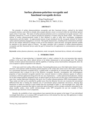
![Fig. 1. (a) A surface plasmon-polariton waveguide structure. (b) Front view and (c) side view with dimensions.
2. PRINCIPLES OF SPP WAVEGUIDES AND THEIR FUNCTIONAL DEVICES
SPP single-mode waveguides are sub-wavelength components in miniaturized opto-electronic circuits that may
either be used to guide plasmonic signals to various parts of the circuit or be used to actively control guided waves.
2.1 Waveguide geometry
SPP single-mode waveguides may be constructed with a thin lossy metal film-stripe of thickness h, length l and
finite width w embedded in a dielectric medium (Fig. 1). The symmetrically divided upper and lower dielectric media
have an equal thickness of d and the whole structure is placed on a substrate [Fig. 1(b)].
In view of functional waveguide devices, the metal-dielectric hybrid waveguide structure is used, where the
dielectric is treated as another waveguide. Thus, propagating modes in this dielectric can be controlled by SPP modes, or
vice versa.
2.2 Nature of SPP modes
A SPP mode may be excited by the end-coupling or pig-tailing method, where a light-wave is fed onto the polished
or cleaved metallic waveguide end-face, with the input light-wave profile matching closely to that of the guided-wave.
This light, having a frequency of ω, then interacts with mobile surface electron-charges that have a frequency of ωp to
give rise to the electromagnetic SPP mode with an enhanced field strength that is confined to the nano-scale dimension
of the metal surface. This confined SPP mode, with ω<ωp, is thus tightly bound to the planar metal surface, is guided by
this surface and propagates with its energy dissipating as heat as a result of electron-lattice imperfection collisions in the
metal. These ohmic losses consequently limit the propagation distance, z, of SPP modes; on the other hand, the mode-
field decays exponentially in the surrounding upper and lower dielectric media, away from the surface, in the x-direction
normal to metal-dielectric interfaces (Fig. 2). Thus, the dielectric media must be sufficiently thick to include all the fields
inside; on the other hand, the metal film-stripe must be sufficiently thin so that the two SPP electric mode-fields
associated with the upper and the lower interfaces overlap and couple with each other efficiently to form two
fundamental SPP stripe-modes, of which the lower-energy tangential, or symmetric, mode (upper and lower SPP mode-
fields in-phase with one another) is considered here for applications purposes. By varying the thickness of the metal
film-stripe, the frequency and the wavelength, λ, of this stripe-mode can be varied.
The use of a dielectric gain medium can compensate for metal losses, allowing SPP modes to propagate along the
metallic nano-structure without loss. In the metal-dielectric hybrid waveguide structure, energy can be transferred from
the dielectric gain medium to the propagating SPP mode, localizing it in the metal surface; while the thin metal film-
stripe confines the lasing mode to the dielectric gain medium, with the SPP mode guiding the lasing mode. Other
methods of realizing functional SPP waveguide devices may be found in [2,15].](data:image/gif;base64,R0lGODlhAQABAIAAAAAAAP///yH5BAEAAAAALAAAAAABAAEAAAIBRAA7)
More Related Content
What's hot
What's hot (20)
Viewers also liked
Similar to Paper 7218 52
Similar to Paper 7218 52 (20)
Recently uploaded
Recently uploaded (20)
Paper 7218 52
- 1. Surface plasmon-polariton waveguide and functional waveguide devices Wing-Ying Kwong* P.O. Box 3115, Spring Hill, FL 34611, U.S.A. ABSTRACT The principle of surface plasmon-polariton waveguides and their functional devices, realized by the hybrid waveguide structure, used within an already ultra-compact photonic circuit is reviewed within the mid-infrared spectral region at the 2-5 µm range. The nature of surface plasmon-polaritons exist in a symmetrical waveguide structure is first described, followed by a review of optical and physical properties of metals using the Drude model. The dispersion relation of surface plasmon-polariton modes is then obtained in order to study their wavelengths, propagation characteristics and skin depths. An approximated amount of gain introduced into the waveguide structure for lossless surface plasmon-polariton propagation is reviewed. Waveguide characteristics, including losses minimization and trade- offs are also studied, followed by looking at some of low-loss dielectric, metal and meta- waveguide materials suitable for operation in the spectral region of interest. The paper concludes with a summary of surface plasmon-polariton waveguides and their functional devices under the goal of minimal loss for applications in communications and signal processing. Keywords: surface plasmon, plasmonic, nano-photonic, metal, waveguide, functional device, infrared, sub-wavelength 1. INTRODUCTION The influence of nano-technology in integrated optics is today’s solution for the ever-increasing data capacity problem; at the same time, allows optical devices to be further miniaturized to sub-wavelength sizes. The reduced number of electro-optical interconnections and the capability of realizing various functionalities subsequently allow the cost of expensive optical components to be reduced. At the nano-scale level, surface effects take place. Fascinating phenomena occur when light-matter interact in nano- structures, with materials exhibit fascinating optical properties at the surface that cannot exist in their bulk counterpart. In a conventional functional waveguide device, a guided mode is controlled by an external input signal applied to the control-electrode that is placed on top of the dielectric waveguide. Recently, investigations into electromagnetic properties of nano-structured waveguide materials have renewed interests in surface plasmons (quanta of collective excitations), with their applications being led to the new area of plasmonics surface-plasmon-based photonics. Indeed, for an ultra-compact photonic integrated circuit, an optical signal can also be sent over this active control-electrode at the same time, causing light-metal interaction that gives rise to surface plasmon-polariton (SPP) electromagnetic modes. These modes not only can be controlled by guided waves from the dielectric but also can overcome the conventional diffraction-limit that is limiting the minimum size of conventional optical components and devices, allowing their dimensions to further be reduced to much smaller than the wavelength of light; i.e. sub-wavelength sizes. These SPP modes have greater momentum than light at a particular optical frequency and are strongly confined to and guided by the planar metallic surface, where mobile electron-charges reside. SPP waveguides are just one example of these miniaturized opto-electronic circuit components. Recently, the availability of new semiconductor laser materials that can operate in the longer 2-5 µm mid-infrared wavelength band allows us to construct SPP waveguide devices with minimal loss that may find applications in (data) communication and signal processing industries. *kwong_wing_ying@email.com
- 2. Fig. 1. (a) A surface plasmon-polariton waveguide structure. (b) Front view and (c) side view with dimensions. 2. PRINCIPLES OF SPP WAVEGUIDES AND THEIR FUNCTIONAL DEVICES SPP single-mode waveguides are sub-wavelength components in miniaturized opto-electronic circuits that may either be used to guide plasmonic signals to various parts of the circuit or be used to actively control guided waves. 2.1 Waveguide geometry SPP single-mode waveguides may be constructed with a thin lossy metal film-stripe of thickness h, length l and finite width w embedded in a dielectric medium (Fig. 1). The symmetrically divided upper and lower dielectric media have an equal thickness of d and the whole structure is placed on a substrate [Fig. 1(b)]. In view of functional waveguide devices, the metal-dielectric hybrid waveguide structure is used, where the dielectric is treated as another waveguide. Thus, propagating modes in this dielectric can be controlled by SPP modes, or vice versa. 2.2 Nature of SPP modes A SPP mode may be excited by the end-coupling or pig-tailing method, where a light-wave is fed onto the polished or cleaved metallic waveguide end-face, with the input light-wave profile matching closely to that of the guided-wave. This light, having a frequency of ω, then interacts with mobile surface electron-charges that have a frequency of ωp to give rise to the electromagnetic SPP mode with an enhanced field strength that is confined to the nano-scale dimension of the metal surface. This confined SPP mode, with ω<ωp, is thus tightly bound to the planar metal surface, is guided by this surface and propagates with its energy dissipating as heat as a result of electron-lattice imperfection collisions in the metal. These ohmic losses consequently limit the propagation distance, z, of SPP modes; on the other hand, the mode- field decays exponentially in the surrounding upper and lower dielectric media, away from the surface, in the x-direction normal to metal-dielectric interfaces (Fig. 2). Thus, the dielectric media must be sufficiently thick to include all the fields inside; on the other hand, the metal film-stripe must be sufficiently thin so that the two SPP electric mode-fields associated with the upper and the lower interfaces overlap and couple with each other efficiently to form two fundamental SPP stripe-modes, of which the lower-energy tangential, or symmetric, mode (upper and lower SPP mode- fields in-phase with one another) is considered here for applications purposes. By varying the thickness of the metal film-stripe, the frequency and the wavelength, λ, of this stripe-mode can be varied. The use of a dielectric gain medium can compensate for metal losses, allowing SPP modes to propagate along the metallic nano-structure without loss. In the metal-dielectric hybrid waveguide structure, energy can be transferred from the dielectric gain medium to the propagating SPP mode, localizing it in the metal surface; while the thin metal film- stripe confines the lasing mode to the dielectric gain medium, with the SPP mode guiding the lasing mode. Other methods of realizing functional SPP waveguide devices may be found in [2,15].
- 3. Fig. 2. Field amplitudes of a surface plasmon-polariton wave normal to metal-dielectric interfaces. 2.3 Properties of metals Because metals play a major role in SPP waveguides and their devices, it is worthwhile to review some of the properties of metals separately. The theory of optical properties of metals may be deduced from the Drude model that treats free electrons in metals as oscillators. Initially, the metal consists of stationary positive ions and a gas of free electrons that are in equilibrium with one another; the total charge within such a plasma volume is zero and there is no force acting on any conduction electrons. When an external field is applied, the free electrons experience a force and accelerate, drifting with a steady velocity in the direction of the applied field. These drifting electrons collide with heavy ions that are located at irregular- lattice points and transfer their energy and momentum to these lattice imperfections. Consequently, thermal vibrations of ions about their equilibrium positions and damping of the electron motion are resulted. The electrons then re-start the acceleration, drifting in the direction generally opposite to the applied field. The Drude model solves the equation of motion under an applied electric field, E, to give the displacement of an electron from its initial position or from an ion; this displacement gives rise to an electric dipole moment. For a volume of electrons, a volume density of electric dipole moments is obtained; thus, the expression for this induced electric polarization, P, in the metal may be written as P (ω ) = ε 0 χ e (ω ) E (ω ) , (1) where χe is the electric susceptibility. Applying Eq. (1) to the electric displacement relation, D, one obtains D (ω ) = ε 0 E (ω ) + P (ω ) = ε 0ε m (ω ) E (ω ) , (2) where εm(ω) is the dielectric function or relative permittivity of the metal and is given as 2 ωp ε m (ω ) = 1 + χ e (ω ) = 1 − 2 , (3) ω − jΓ ω where ωp is the angular plasma frequency that characterizes the metal and Γ is the mean time between electron collisions with lattice thermal vibrations or the scattering rate of the electron. The equivalent permittivity of the plasma, εp(ω), may then be defined as ε p (ω ) = ε 0ε m (ω ) . (4)
- 4. Based on Eq. (3), one may also obtain the intrinsic impedance of the plasma, ηp(ω); thus, η0 η0 η p (ω ) = = ε m (ω ) ωp 2 , (5) 1− 2 ω − jΓ ω where η0 is the free space intrinsic impedance. The Drude model assumes that the metal is a good or an ideal conductor. Predictions from this model quite agree with reported experimental data for most metals at wavelengths of 1 µm and longer, which covers nearly the whole infrared spectrum. Optical properties of metals are characterized by the complex refractive index, nm, of an absorbing medium, n m = n ′ − jκ , m (6) where nm′ is the index of refraction and κ is the extinction coefficient that is responsible for the evanescence of an optical wave. Both optical constants, nm′ and κ, are wavelength- and temperature- dependent. At optical frequencies, εp is a complex number and is related to nm by ε0nm2. Matching this relation with that in Eq. (4), one obtains 2 ε m = nm , (7) 2 2 2 ε m − j ε m = ( n ′ − jκ ) = ( n m − κ ) − j 2 n ′ κ . ′ ′′ m ′ m (8) Matching dielectric constants with optical constants, one obtains 2 2 ′ ′ ε m = nm − κ and (9a) ′′ ′ ε m = 2 nm κ , (9b) where εm″ is responsible for the absorption and scattering losses in the metal. From Eq. (8), one may also solve for optical constants in terms of dielectric constants, yielding n′ = 1 [ ε m + ε m + ε m ] and 2 ′2 ′′ 2 ′ (10a) m 2 κ = 1 [ εm + εm − εm] , 2 ′2 ′′ 2 ′ (10b) 2 where εm′ and εm″ may be obtained from Eq. (3) as 2 ωp ′ εm = 1− 2 2 and (11a) ω +Γ 2 ω pΓ ′′ εm = 2 2 . (11b) ω (ω + Γ ) For nm′<<κ, reflectivities of light from metal surfaces are nearly 100%, particularly at the end-coupling excitation type of incidence. For an ideal metal, nm′=0, nm2=-κ2<0 and εm=εm′<0; propagating light-wave is always evanescent and the reflectivity of light from such a metal surface is always 100%. Such metal provides the total reflection for well-confined mode propagation. In addition, if the metal surface is an ideal surface, incident light cannot excite surface plasmons on
- 5. such a surface; however, mechanisms must be used in order to couple these non-radiative surface plasmons with external electromagnetic radiations, such as the use of surface roughness or a grating and the attenuated total reflection method15. One of the physical properties of interest for metals is the crystal structure, which is important when stability comes into concern. Crystals with cubic and hexagonal structures exhibit anisotropies (structure-type dependent) that do not appear in the polycrystalline structure. Polycrystalline metals are of random texture that may be induced by growth and processing conditions. Nearly all common metals are polycrystalline. For wavelengths between 2 to 5 µm, nm′<<κ or εm has a large negative εm′ and a small positive εm″ at room temperature. Table 1 lists calculated refractive indices and relative permittivities of selected polycrystalline metals at λ=3.10 µm at room temperature. Table 1. Calculated refractive indices and relative permittivities. Metal nm εm Beryllium 2.07-j12.6 -154.48-j52.16 Copper 1.59-j16.5 -269.72-j52.47 Gold 1.73-j19.2 -365.65-j66.43 Tungsten 1.94-j13.2 -170.48-j51.22 2.4 SPP waveguide parameters The metal surface of interest in this paper is of the continuous planar metal surface type having a refractive index of nm embedded in a dielectric that has a refractive index of n d [Fig. 1(b)]. From optical waveguide theory, the propagation constant, β, may be found by solving the mode condition for TM SPP mode and is given as 2 2 nm n d β = k0 2 2 , (12) nm + n d where k0=ω/c is the free space wave-number of a light-wave. (TE SPP modes were proven non-existent at the metal- dielectric interface7.) As this fundamental SPP mode propagates along the metal-dielectric interface, the mode-power attenuation causes β to become complex; i.e. β = β′− j α , (13) 2 where β′ is the real propagation constant and α is the power attenuation coefficient. By substituting Eq. (6) into Eq. (12) and using the binomial approximation, one obtains 2 2 nd ( n′ − κ ) m 2 n′ κnd m 2 β ≈ k0 2 2 2 1− j 2 2 2 2 2 . (14) ′ nm + n d − κ ( n′ − κ )( n′ + nd − κ ) m m In order to evaluate dispersion characteristics of SPP modes, one re-writes Eq. (12) using n d2=εd, where εd is the relative permittivity of the dielectric and Eq. (7) to give the dispersion relation for the SPP propagation, ω ε mε d k spp = ; (15) c εm + εd where kspp is the wave-vector component of SPP modes that is parallel to the interface. Confined SPP mode propagation requires that εmεd<0 and εm+εd<0, so that kspp is real. For the spectral region of interest, one may assume |εm′|>>|εm″| and | εm′|>>|εd|. The dielectric medium should not be significantly dispersive, so that k spp/k0 is always slightly larger than unity for |εm|>>|εd|; i.e. kspp>k0, which implies the momentum (ħk) of SPP modes is always slightly greater than that of light in free space.
- 6. Since εm is complex, this implies kspp is also complex. Using Eqs. (9) to re-write Eq. (14) in terms of dielectric constants, one obtains the complex kspp as ε dε m ′ ′′ ε mε d ′ ′′ k spp = k spp − jk spp ≈ k 0 1 − j ′ . (16) ′ εd + εm ′ 2ε m (ε d + ε m ) Matching the real and the imaginary parts of this equation with those of Eq. (13), one obtains ′ εdεm k spp ≡ β ′ = k 0 ′ and (17a) ′ εd + εm 3 α k0 ′′ ε mε d 3/ 2 ε mε d ′′ k0 ε m ′ 2 ′′ k spp ≡ ≈ = 2 (17b) 2 2 ′ ′ ε m (ε d + ε m ) 3 ′ ′ 2 εm εm + εd respectively. kspp′ gives the wavelength of the SPP mode, λspp and kspp″ gives the propagation length of the SPP mode, δspp the distance that the SPP propagates before its power or intensity is reduced by 1/e=0.368. Using the relation k=2π/λ on Eq. (17a), one obtains 2π ′ εm + εd λspp = = λ0 . (18) ′ k spp ′ ε mε d For |εm′|>>|εd|, λspp is slightly less than λ0; i.e. λspp<λ0, which suggests possible applications in sub-wavelength electromagnetic waveguiding. The SPP propagation length may be found by using the relation δ=1/α with Eq. (17b), yielding 3 λ0 ε m ε m + ε d 2 1 ′2 ′ δ spp = = . (19) ′′ 2k spp 2π ε m ε mε d ′′ ′ Comparing this equation with Eq. (18), one can see that δspp>>λspp, implying that one may use periodic surface structures (such as gratings) to manipulate SPPs, allowing these modes to interact with such structures over several periods. In a plasmonic circuit, an optical signal faded away during transmission in the SPP waveguide, before reaching the destination, because of the conventional short propagation length. To increase the propagation length, one may choose a low-loss or a high plasmonic resonance (εm′2/εm″>>1) metal, such as copper, gold or silver, or may decrease the metal film thickness in order to decrease the attenuation of the SPP mode, but with the mode-field extends further into the dielectric. Sufficiently thin metal film thickness should be on the order of 50 nm for most metals at optical frequencies in order to support the single stripe SPP-mode propagation. From ray optics, the propagation constant in the wave-normal direction may be written as 2 2 2 2 k i = ε i k 0 = k x ,i + k spp , i=d,m, (20) where 2 2 2 εi k x ,i = k 0 (21a) εm + εd is the mode-field attenuation constant in the x-direction and
- 7. 2 2 ε mε d k spp = k 0 (21b) εm + εd is the propagation constant in the z-direction. Since kspp2>ki2=εik02, kx,i must be imaginary, which explains the evanescent tails of mode-fields extended into the two media in the x-direction. Penetration depths, or attenuation lengths, of SPP mode-field into the dielectric, δd and into the metal, δm, may be found by taking the inverse of their respective attenuation constant; i.e. δi=1/kx,i, i=d,m the distance at which the mode-field strength attenuated by 1/e and is given as 1 1 εm + εd δd = = 2 , (22a) k x,d k0 εd 1 1 εm + εd δm = = 2 . (22b) k x,m k0 εm For k0=2π/λ0, as the free space wavelength increases, δi also increases. In addition, for |εm|>>|εd|, δd is proportional to √| εm|; by inspection, as |εm| increases, δd increases, implying that the field penetrates deeper into the dielectric. Typically, δd>100 nm. If metallic nano-particles are used instead of continuous planar metal surfaces, δd can be reduced considerably. Structures constructed with an array of metallic nano-particles may be found in [6,11]. Similarly, δm is inversely proportional to √|εm|; by inspection, as |εm| increases, δm decreases, implying the minimum metal film thickness to be used. In SPP-based nano-circuits, δm≈10 nm, which is a much shorter length-scale than 50 nm. Thus, the metal thin-film can no longer simply be described by a relative permittivity; rather, there are two factors to be considered when describing the optical response of such ultra-thin metal-films: (1) a non-local or spatially dispersive response of a nearby object, such as a molecule, must be included (due to the possibility that the molecule may lose its energy to the SPP mode) in order to define such a small δm, over which an impedance mismatch occurs and (2) for fields that penetrate from the dielectric into the metal, this impedance mismatch at the metal-dielectric interface can significantly reduce the penetrated field-strength in the metal, resulting in a length scale much less than δm. This new description of an ultra-thin metal-film had given us the idea that the metal-dielectric boundary is not definitive. 2.5 SPP propagation in the presence of gain In order to compensate for ohmic losses in the metal, gain is introduced into the dielectric medium to improve the propagation length or to achieve lossless propagation. This causes the relative permittivity of the dielectric to become complex; i.e. εd=εd′+jεd″ and dispersion relations in Eqs. (21) becomes 2 2 2 (ε i′ − jε i′′) k x ,i = k 0 , i=d,m and (23a) (ε m + ε d ) − j (ε m − ε d′ ) ′ ′ ′′ ′ 2 2 (ε m − jε m )(ε d + jε d′ ) ′ ′′ ′ ′ k spp = k 0 , (23b) (ε m + ε d ) − j (ε m − ε d′ ) ′ ′ ′′ ′ where εi″>0 for a lossy metal and εi″<0 for a gain dielectric. Because εm′ is negative and |εm′|>>|εd|, one may assume that | εm′|>>|εd′|,|εd″|. Separating Eq. (23b) into real and imaginary parts, assuming a high plasmonic resonance metal is used, one obtains 2 ( ) 2 εm 2 2 k0 2 2 k spp ≈ ε′ ε 2 d m ′ + εm εd + j ( −ε m ) ε ′′ − ′′ ε ′′ + ε ′ 2 , (24) ′ ′ (ε m + ε d ) d ε ′′ d d m
- 8. where |εi|2=(εi′)2+(εi″)2, i=d,m. To find the amount of gain that fully compensates metal losses for lossless propagation, one sets the imaginary part of Eq. (24) to zero and solves for εd″, yielding 2 ′′ ′ ε mε d ε d′ ≈ ′ 2 ; (25) εm thus, the complex εd becomes εd′+j[(εm″εd′2)/|εm|2]. By inspection, higher plasmonic resonance implies lesser gain is required for lossless propagation. The power gain coefficient, g, may be obtained by interchanging the subscripts d and m in Eq. (17b), followed by linearly transforming α via a sign change (g=-α). Under the condition that |εm|>>|εd′|, one obtains ε d′ ′ g = − k0 . (26) ′ εd Substituting Eq. (25) into Eq. (26) for lossless propagation and using the definition of k0, one obtains the required gain, g0, to compensate for metal losses as ′′ ′ 3 / 2 2π ε m (ε d ) g0 = − 2 . (27) λ0 εm Thus, as gain is added into the dielectric, the propagation length begins to increase; until |g|=|g0|, lossless SPP propagation is achieved. As gain represents a loss in the dielectric, gain requirements should be as low as possible. By inspection of Eq. (27), the wavelength-band of interest clearly has a lower gain requirement than shorter wavelengths in the mid-infrared band, such as the telecommunication wavelength of 1.55 µm, because of the λ0-1 dependence; also, as εd′ decreases, g0 decreases, suggesting that a lower refractive index for the dielectric may be used to reduce the gain requirement. 2.6 SPP waveguide characteristics In practice, besides absorption losses in metals, one should take into account additional losses, such as scattering losses (due to surface roughness and metal-stripe edges) and grain boundaries, which can increase the gain requirement. Advanced deposition techniques, such as nano-fabrication, and good surface quality may improve the gain requirement and should be carefully considered when preparing samples. Furthermore, scattering and absorption in the dielectric also contribute to propagation losses. The insertion loss associated with metal electrodes should also be reduced. By using a buffer layer of low refractive index (e.g. a layer very similar to the dielectric gain layer in chemical composition) to relax the metal’s effect on guided modes, propagation loss due to the metal-dielectric interface can be reduced to an insignificance; i.e. propagation loss decreases abruptly as the buffer layer thickness increases. The symmetrical SPP waveguide structure offers the lowest SPP propagation loss among SPP waveguide structures having proper dimensions. For a functional SPP waveguide device, where another guided wave, excited by an external optical excitation or a temperature change in the dielectric medium, interacts with the SPP mode, the waveguide structure becomes asymmetric as a consequence of the refractive index change. SPP modes then suffer an additional radiative loss that decreases the propagation length. Since the SPP propagation loss depends on the refractive-index difference between top and bottom dielectric layers, the larger the asymmetry, the higher the propagation loss. This asymmetry causes the SPP mode depth profile (depth mode-field diameter, DMFD) to change from a symmetric profile to an asymmetric profile as well. When the asymmetry increases beyond some limit, the SPP mode-character is lost and the SPP waveguide then becomes a conventional slab waveguide. The DMFD, depending on the thickness of the metal stripe, determines the tightness of the SPP mode that is bound to the metal-surface and can be tuned by the thickness of the dielectric. Reducing the dielectric thickness increases the propagation loss; so does reducing the metal film thickness, but it allows the mode to become better confined. Thus, there is a trade-off between mode size and propagation loss.
- 9. A metal film-stripe with a finite width, w [Fig. 1(c)], is treated as a core surrounded by a dielectric. Generally, the propagation loss decreases as w decreases, indicating a very low propagation loss may be achieved by reducing w. However, when w becomes much narrower than a wavelength, no guided modes can exist in the metal stripe, limiting the propagation on the stripe. Nevertheless, for micrometer-wide stripes, the lateral MFD, LMFD, depending on w, determines the confinement of the SPP mode. Reducing w causes the LMFD to decrease at the beginning but at some w, starts to increase, showing a poor light confinement with too-narrow metal stripes; while the DMFD increases, decreasing the propagation length. From these features of SPP-mode depth and lateral profiles, one may conclude that coupling losses at one end of the metal stripe waveguide will increase as w decreases. Therefore, by choosing a proper metal film-stripe dimension, one can reduce the coupling loss, with SPP mode profiles matching closely with those of the incident mode. Besides introducing gain into the dielectric medium to compensate for ohmic losses in metals, the volume of the metal itself can be reduced to its smallest possible dimension in order to reduce ohmic losses. On the other hand, the high reflection from metals can be compensated by matching impedances on metals. 3. SPP WAVEGUIDE MATERIALS For high efficient functional waveguide devices, careful selection of practical materials not only minimizes losses, such as propagation loss and transmission loss (induced by the internal damping of the SPP mode due to the resistive heating in the metal), but also facilitates fabrication processes. An optimally low propagation loss requires an optically transparent material with a minimal surface roughness and guided-wave scattering; this material should also be highly purified after fabrication processes in order to avoid unnecessary absorption by impurities. 3.1 Dielectric gain materials In an effort to offer a structure for SPP propagation comparable to an optical fiber, the SPP waveguide structure can be obtained by spin-coating solutions of laser dye molecules or π-conjugated polymers before and after the metal thin- film-stripe deposition. Laser gain materials can compensate metal losses; while polymers are known for meeting low- cost, easy fabrication, flexibility and high performance requirements. For wavelengths in the 2-5 µm spectral region, the operative low-loss dielectric gain material system includes fluorides, chalcogenides, halides and III-V compound semiconductor nano-crystals. Because of the λ-4 dependence of the Rayleigh scattering loss in these materials, it is possible to obtain an extremely low transmission loss. The lowest loss for fluorides occurs at wavelengths in the 2-4 µm region, which has a loss value 10-100 times lower than that for the traditional silicide materials. Silicides have their lowest loss occurs at λ=1.55 µm. Some of the superior optical characteristics of fluorides include very low index of refraction, scattering and absorption. Chalcogenides, compounds include chalcogen (S, Se, Te), exhibit a large acousto-optic figure-of-merit (FOM) and a changeable refractive index by light, which are advantageous to functional waveguide devices; however, the index change is strongly dependent on the fabrication method and thermal history. Optical constants of chalcogenides can be tailored by material composition and transmission losses are wavelength-, composition- and substrate- dependent. An example of chalcogenides is the lead sulphide, which can operate at a wavelength in the neighborhood of 3 µm at room temperature. Halide crystals, compose of CaF2, can be used to manufacture HF laser gain materials that operate at λ=3 µm. The InAs- and GaSb- based III-V compound semiconductors possess superior electrical, thermal and optical characteristics, strong chemical bonds and low dielectric constants; these semiconductors can be processed at high- temperatures and grown into high-quality thin-films. Examples of III-V quaternary semiconductors are GaInAsSb and InPAsSb.
- 10. 3.2 Metals At optical frequencies, the choice of a metal for the SPP waveguide structure becomes crucial. To find a metal with low losses, one may use the FOM to measure; i.e. FOM=-(nm′/κ). Among polycrystalline metals, the three candidate metals for lowest losses at 2-5 µm wavelength band were found to be silver, gold and copper, respectively, with silver exhibits the lowest loss. In addition, these three face-centered cubic metals have the lowest resistivities and the highest conductivities, with silver having the highest electrical and thermal conductivities among all metals, followed by copper. Silver also has a high reflectivity. In general, pure metals have their resistivities increased with increasing amounts of alloying elements. For a metal thin-film, a deposited coating almost always has a higher reflectance than a polished or electroplated surface; if optical properties are varied, reflectance and absorptance also vary, which may cause measurements of scattering from polished surfaces to be off-scaled with wavelengths, compare to those from surface roughness. 3.3 Metamaterials Discovered in less than a decade ago, this artificial negative-index material was found to have the capability of mimicking the response of a metal to electromagnetic waves when ω<ωp, i.e. the negative εm. An early example of a metamaterial is one that has its negative εm obtained by arranging long and thin wires in a simple cubic lattice and its negative permeability obtained from the split-ring resonator14. Metamaterials, having pre-designed properties, allow both electric- and magnetic- field components of light to be coupled with meta- atoms and molecules; i.e. inclusions smaller than a wavelength. The shape and size of these engineered materials can be tailored and their composition, morphology and resonances can be artificially and separately tuned. Meta- atoms and molecules can be designed and replace atoms and molecules in a conventional material at desired locations to achieve new functionalities. In addition, metamaterials offer nearly no reflectance. These fascinating unprecedented electromagnetic properties and functionalities promise to open up a new prospect in manipulating light, revolutionizing today’s optical technologies. 4. CONCLUSION For an efficient optical data communication, the most important factor is to minimize propagation losses and transmission losses. At wavelengths in the 2-5 µm mid-infrared region, SPP waveguides, with a structure of a nanometer thin polycrystalline metal embedded in a dielectric gain medium, offer the possibility to transmit plasmonic signals with negligible, or without, losses; the SPP mode is excited by the end-coupling method. Active control of SPP signals in functional SPP waveguide devices of the metal-dielectric hybrid waveguide structure is implemented by guided-wave control from the dielectric. By optimizing the SPP waveguide geometry and careful selection of waveguide materials, one can further reduce the gain requirement for a lossless SPP transmission and further minimize other losses, enabling SPP-based functional waveguide devices to operate with a supreme efficiency. With the development of the state-of-the- art nano-scale fabrication techniques such as nano-lithography, low-cost sub-wavelength nano-photonic components can be mass-produced, evolving to the efficiency of semiconductor fabrication.
- 11. REFERENCES [1] Bozhevolnyi, S. I. and Shalaev, V. M., "Nanophotonics with surface plasmons - Part I," Photonics Spectra 40(1), 58-66 (2006). [2] Ozbay, E., "Plasmonics: merging photonics and electronics at nanoscale dimensions," Science 311, 189-193 (2006). [3] Boltasseva, A., Nikolajsen, T., Leosson, K., Kjaer, K., Larsen, M. S. and Bozhevolnyi, S. I., “Integrated optical components utilizing long-range surface plasmon polaritons," J. Lightwave Technol. 23(1), 413-422 (2005). [4] Bass, M., editor-in-chief, [Handbook of Optics], 2nd ed., McGraw-Hill, Inc., New York (1995). [5] Barnes, W. L., "Surface plasmon-polariton length scales: a route to sub-wavelength optics," J. Opt. A: Pure Appl. Opt. 8, S87-S93 (2006). [6] Atwater, H., “Guiding light,” Oe magazine 2(7), 42-44 (2002). [7] Yariv, A. and Yeh, P., [Optical Waves in Crystals], John Wiley & Sons, Inc., New York, 405-503 (1984). [8] Nezhad, M., Tetz, K. and Fainman, Y., "Gain assisted propagation of surface plasmon polaritons on planar metallic waveguides," Opt. Express 12(17), 4072-4079 (2004). [9] Nishihara, H., Haruna, M. and Suhara, T., [Optical Integrated Circuits], McGraw-Hill Book Co., New York (1989). [10] Su, P. S., compiled, [Materials Advanced Technology], Fu Han Publishers, Tainan, 4-7 (1994). [11] Lal, S., Link, S. and Halas, N. J., “Nano-optics from sensing to waveguiding,” Nature Photonics 1, 641-648 (2007). [12] Wu, J. W., “Long-wavelength optical semiconductor materials,” <http://ykuo.ncue.edu.tw/report/017-Long- Wavelength%20Optical%20Semiconductor%20Materials.doc> (2007). [13] Shalaev, V. M., “Optical negative-index metamaterials,” Nature Photonics 1, 41-48 (2007). [14] Soukoulis, C. M., Linden, S. and Wegener, M., “Negative refractive index at optical wavelengths,” Science 315, 47-49 (2007). [15] Pitarke, J. M., Silkin, V. M., Chulkov, E. V. and Echenique, P. M., “Theory of surface plasmons and surface- plasmon polaritons,” Rep. Prog. Phys. 70, 1-87 (2007). [16] A. Lakhtakia (private communication).