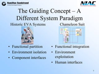
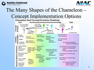
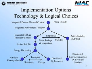
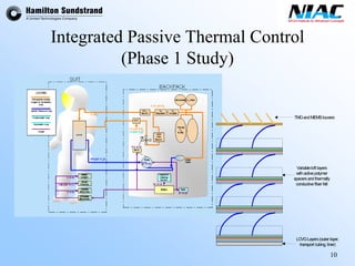
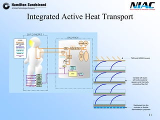
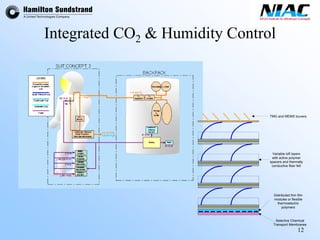
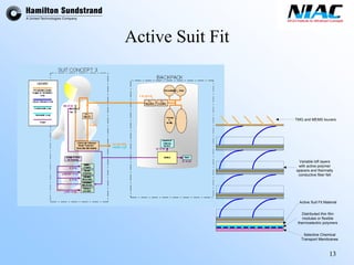
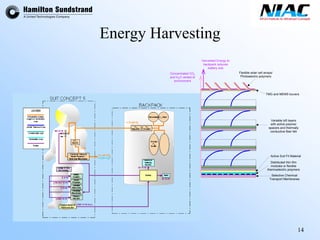
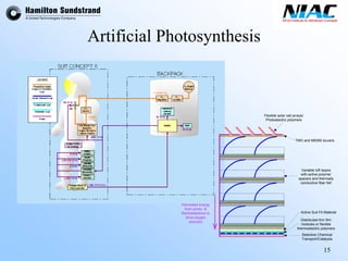
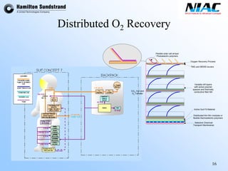
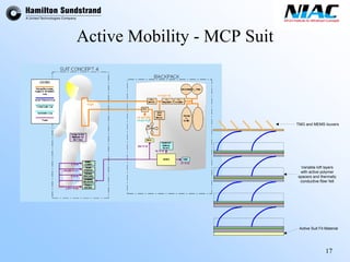
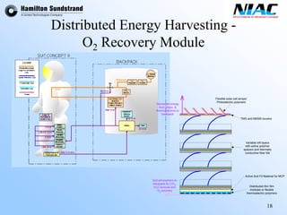
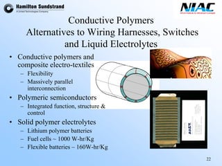
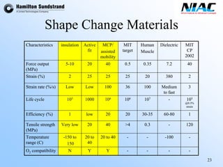
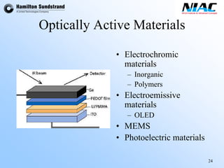
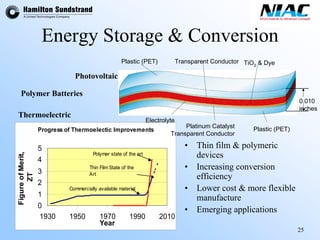
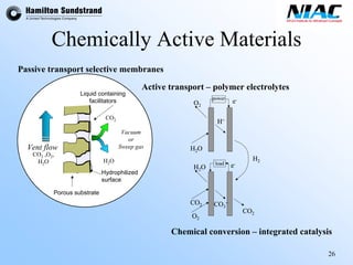
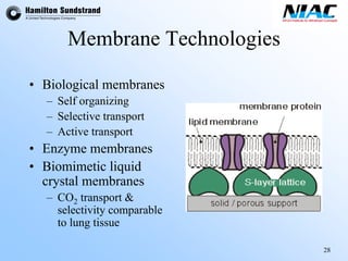
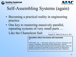
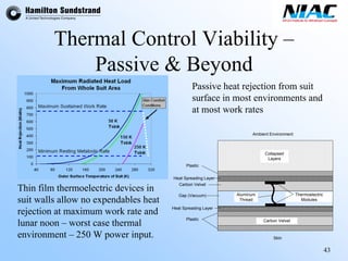
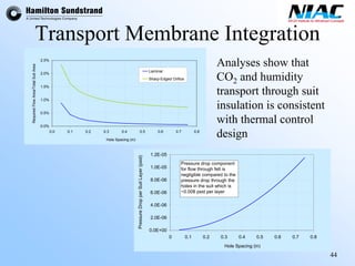
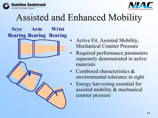
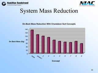
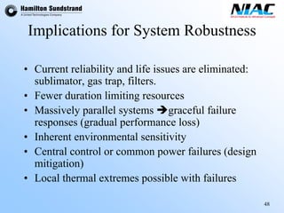
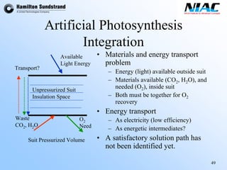
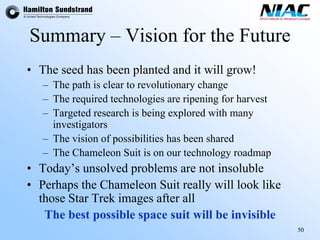
The document discusses the concept of a "Chameleon Suit" that aims to revolutionize extra-vehicular activity (EVA) systems through an integrated, multi-functional design approach. It outlines some of the key challenges with current EVA systems and opportunities emerging technologies provide to address issues like mobility, thermal control, life support and energy needs. The concept integrates functions like thermal regulation, gas transport and power generation directly into the suit material through the use of advanced materials like conductive polymers, shape memory alloys and thin film devices. While challenges remain around issues like artificial photosynthesis integration, the document argues the required technologies are advancing and a fully-integrated, lightweight suit that improves upon current systems is achievable.
This lecture discusses nanotechnology applications in aerospace, focusing on carbon nanotubes. Carbon nanotubes have excellent mechanical and electrical properties and are being investigated for use in high-strength, lightweight composites for aircraft. The lecture will cover the properties of carbon nanotubes and their current and potential uses in aerospace composites, sensors, coatings and other applications. It will also discuss challenges in dispersing carbon nanotubes uniformly in composite matrices.
Aml series piezoelectric materials green energy and sensing - crossing pointMariya Aleksandrova
The document discusses piezoelectric materials for energy harvesting and sensing applications. It outlines current trends toward developing flexible thin-film piezoelectric devices that can efficiently convert small vibrations or forces into electrical energy. Several lead-free piezoelectric materials are investigated for these applications including potassium niobate, gallium-doped zinc oxide, and barium strontium titanate. The document evaluates the performance of thin films of these materials for energy harvesting and sensing when deposited under different conditions. Flexible devices using these materials show potential for applications that require compact, lightweight, and battery-free operation.
This PhD thesis investigates the integration of YBa2Cu3O7-x (YBCO) superconducting films with silicon substrates using buffer layers. Cerium oxide (CeO2) and yttria-stabilized zirconia (YSZ) are chosen as buffer layers due to their structural compatibility with silicon and YBCO. Various multilayer structures including CeO2/Si, YSZ/Si, CeO2/YSZ/Si, YBCO/CeO2/Si and YBCO/CeO2/YSZ/Si are grown using magnetron sputtering and characterized structurally and electrically. The goal is to optimize the structural properties at the interfaces and
The document discusses recent trends in photonic devices. It begins by defining optics and photonics, and describes some applications of photonics including information technology, healthcare, sensing, lighting and displays. It then explains that photonic devices manipulate or detect light, providing examples like lasers, LEDs and solar cells. The document goes on to discuss latest trends like nanophotonics using graphene, carbon nanotubes and photonic crystals. It also covers silicon photonic devices using silicon-germanium transistors and germanium-tin phototransistors. In conclusion, it predicts future applications of photonics in areas like e-paper, solar panels and light-emitting fabrics.
Dr. Gernot S. Pomrenke presents an overview of his program, Photonics and Optoelectronics, at the AFOSR 2013 Spring Review. At this review, Program Officers from AFOSR Technical Divisions will present briefings that highlight basic research programs beneficial to the Air Force.
Micro-electro-mechanical systems (MEMS) integrate sensors, actuators and electronics onto a silicon chip through microfabrication. Silicon is commonly used due to its availability and ability to incorporate electronics. MEMS fabrication uses processes like deposition, lithography, etching and bonding. They are used in applications like switches and tunable devices. MOEMS merges MEMS with micro-optics to sense and manipulate optical signals on a small scale. SOI technology uses a layered silicon-insulator-silicon substrate to improve device performance over conventional silicon substrates. Optical switching provides high switching capacity needed for high bit rate transmission.
A review study of mechanical fatigue testing methods for small scale metal ma...Alexander Decker
This document reviews mechanical fatigue testing techniques for small-scale metal materials. It begins by discussing the increased focus on materials behavior at the micro and nano scales due to growing MEMS/NEMS applications. It then classifies fatigue testing techniques for small-scale materials, including uniaxial tension-tension, dynamic bending, and uniaxial tension-compression. Specific techniques are described in more detail, such as using piezoelectric actuators to enable load-controlled uniaxial cyclic loading of thin films. The document also examines fatigue properties of materials tested with these techniques, like studying crack growth rates in nickel alloy cantilever beams under dynamic bending.
This document summarizes research on colloidal CIGS and CZTS nanocrystals for printed photovoltaics. Spray deposition techniques like airbrushing and robotic spraying allow precise control of film thickness and deposition of nanocrystal inks onto flexible plastic substrates. The document describes the synthesis of CIGS nanocrystal inks and how converting the inks to Cu(In,Ga)(S,Se)2 via high-temperature selenization can increase power conversion efficiencies to over 12%. While efficiencies of spray-deposited films are still relatively low for commercialization, the techniques allow for thin-film deposition of inorganic materials under ambient conditions and fabrication of plastic photovol
Nanotechnology is enabling technologies and products at the nanoscale. It is estimated that nanotechnology will generate $4 trillion by 2015. Some key applications discussed include consumer products using silver nanoparticles, flexible solar cells using zinc oxide nanowires and carbon nanotubes, and energy storage devices like supercapacitors using nanocarbons. Research at Cambridge University is exploring new nanocomposite materials for applications in photovoltaics, lighting, batteries, and flexible electronics.
One-Dimensional Carbon Nanostructures—From Synthesis to Nano-electromechanica...Mariana Amorim Fraga
The fundamental properties of one-dimensional (1D) carbon nanostructures and their promising technological applications have stimulated significant research in different areas. Because of their outstanding electrical and mechanical properties, these nanostructures have emerged as a new class of sensor material with real potential for a variety of nano-electromechanical systems (NEMS). Several studies have shown that the performance of a NEMS device is significantly affected by the material properties of the nanostructures used to build it. For this reason, a section of this review is devoted to the synthesis and properties of 1D carbon nanostructures including nanotubes, nanofibers, and nanowires. Thereafter, some NEMS-based sensors using 1D carbon nanostructures are introduced and issues related to their fabrication processes are addressed. The goal of this brief review is to outline the benefits of the use of 1D carbon nanostructures, the current status of development and challenges to enable their widespread application as sensing elements in NEMS devices.
pp. 39-56
S&M1299
http://dx.doi.org/10.18494/SAM.2017.1366
Online Published: January 25, 2017
This document discusses the transfer of micro and nano-photonic silicon nanomembrane waveguide devices onto flexible substrates. It demonstrates transferring optical devices without extra un-patterned silicon onto low-cost, flexible plastic substrates using single-crystal silicon nanomembranes. Specifically, it shows stacking two layers of silicon nanomembranes, with a photonic crystal waveguide in the first layer and multi-mode interference couplers in the second layer, respectively, onto a flexible substrate. This technique promises high density integration of multilayer hybrid structures on flexible substrates.
Nanotechnology involves controlling and manipulating matter at the atomic and molecular scale (typically 1-100 nanometers). It can be used to deal with problems across many fields by exploiting properties that emerge at the nanoscale. Some potential applications of nanotechnology include more effective drug delivery systems, new diagnostic tools in medicine, more efficient energy production and storage, and stronger/lighter materials for vehicles and aerospace uses. The document provides examples of current and potential future uses of nanotechnology in fields like medicine, energy, information technology, and heavy industry.
Micro-electro-mechanical systems (MEMS) are tiny devices that convert electrical energy to mechanical motion and vice versa. There are three key steps to fabricating MEMS: deposition of thin films, patterning of the films, and etching to remove unwanted material. MEMS are commonly used in sensors and actuators due to their small size, low power consumption, and ability to integrate electronics and mechanical elements on a single chip. Common applications include accelerometers in smartphones, pressure sensors in cars, and medical devices.
The document proposes a "Chameleon Suit" concept that would liberate human space exploration by developing a more adaptive spacesuit. It envisions a suit that integrates life support, environmental protection, and mobility functions through emerging technologies. A multi-phase study is outlined to develop the concept through technology exploration, system design, and establishing a roadmap. The goal is a suit that can adapt to environmental conditions, harvest energy from the environment, and potentially regenerate oxygen through artificial photosynthesis.
I hope You all like it. I hope It is very beneficial for you all. I really thought that you all get enough knowledge from this presentation. This presentation is about materials and their classifications. After you read this presentation you knowledge is not as before.
The new IMI Labs service bridges this gap,
opening up the IMI high-throughput
experimentation platform, materials expertise
and analytics to the industry to accelerate and
de-risk the exploration, discovery,
characterization and selection of advanced
materials
The new IMI Labs service bridges this gap,
opening up the IMI high-throughput
experimentation platform, materials expertise
and analytics to the industry to accelerate and
de-risk the exploration, discovery,
characterization and selection of advanced
materials
Nanotechnology involves engineering materials at the nanoscale, around 1 to 100 nanometers. Richard Feynman is considered the father of nanotechnology. Nanotechnology has applications in many fields including electronics, computing, medicine, cosmetics, foods, the military, and energy. By 2020, products with nanotechnology components could be worth $1 trillion. Materials behave differently at the nanoscale compared to larger scales due to statistical mechanics and quantum effects. Nanotechnology is approached through top-down methods like lithography or bottom-up methods like self-assembly.
This document provides an introduction to microelectromechanical systems (MEMS). It defines MEMS as systems that combine electrical and mechanical components on the micrometer scale to sense and control the physical world. MEMS components include microsensors to detect environmental changes, an intelligent component to make decisions based on sensor input, and microactuators to change the environment based on the decisions. Common MEMS applications include accelerometers, inkjet printer heads, medical devices, and sensors in automobiles. The document discusses fabrication techniques like deposition, patterning, and etching used to create MEMS, as well as their advantages like low cost, small size, and high functionality.
Charlotte Lelieveld - Smart Material Systems for Architectural ApplicationsMerford
Een presentatie van Charlotte Lelieveld. Zij is promovendus aan de TU Delft, faculteit Building Technology & Architectural Engineering met een specialiteit in "smart materials". Het onderwerp van deze lezing was slimme materialen. Wat verstaat men onder deze term? Aan de hand van welke eigenschappen kun je deze materialen onderscheiden? Er bestaan passieve en actieve slimme materialen. Voor welke toepassingen zijn deze geschikt? Charlotte schetste tijdens deze presentatie een toekomstbeeld van het gebruik van deze materialen in de architectuur.
Gegeven op dag 7 van Soundbites by Merford met als thema: Slimme Materialen.
http://www.merford.nl/soundbites
Here are the key steps in the Czochralski crystal growth process:
1. High purity silicon is melted in a quartz crucible within a furnace.
2. A small silicon crystal (seed) is lowered into contact with the melt and slowly withdrawn, causing silicon from the melt to solidify onto the seed.
3. The seed crystal is precisely rotated and raised at a controlled rate, forming a solid cylindrical ingot of single crystal silicon.
4. The crystal grows as the seed is pulled upwards, maintaining a solid-liquid interface in thermal equilibrium between the melt and the growing crystal.
5. After growth is complete, the crystal ingot is cooled and processed further for wafer production
This document discusses applications of nanotechnology in electronics and mechanical engineering. It outlines several key areas where nanotechnology can have impact, such as semiconductors, passive components, display materials, and packaging/interconnection. For semiconductors, it describes potential applications like doping carbon nanotubes and creating quantum dots. It also discusses using nanoparticles to fabricate nanowire structures for uses like sensors. For packaging, it notes nanotubes and diamond films can improve thermal performance. The document concludes that over the next five years, significant new nanomaterials and processes will address important industry issues, and longer-term nanotechnology will extend or replace technologies to meet customer needs.
This document discusses applications of nanotechnology in electronics and mechanical engineering. It outlines several key areas where nanotechnology can have impact, such as semiconductors, packaging, boards/substrates, and passive components. For semiconductors, nanotechnology allows for doping of nanotubes and creation of quantum dots. It also discusses using nanotubes for quantum computing. For packaging, nanotubes and diamond films can improve thermal conductivity. The document also outlines several developing applications of nanotechnology in nanoelectronics, such as flexible displays, high-density memory chips, smaller transistors, and novel transistors using graphene and nanoparticles.
The document summarizes discussions from the 25th anniversary conference of the Foresight Nanotechnology Institute. Key topics included the progress and commercialization of nanotechnology over the past 25 years, challenges in the field like cross-disciplinary training and funding high-risk long-term research, and applications of nanotechnology in various industries from aerospace to biomedical. New areas discussed included using synthetic proteins and viral capsids for drug delivery, molecular computing, and mining operations on the moon.
MEMS (micro-electro-mechanical systems) are microscopic devices and integrated systems that combine electrical and mechanical components between 1-100 micrometers in size. They integrate sensors, actuators and electronics on a common silicon substrate through microfabrication technology. MEMS originated in the 1980s and are now used in automotive, biomedical, industrial and consumer applications. Some key advantages of MEMS include lower manufacturing costs, reduced size, and lower power consumption compared to macro-scale devices. Challenges include developing robust packaging and manufacturing processes for commercialization.
This document discusses microelectromechanical systems (MEMS) fabrication methods. It covers common MEMS fabrication processes like deposition, lithography, and etching. Deposition methods include chemical vapor deposition and physical vapor deposition to deposit thin films. Lithography involves transferring patterns to photosensitive materials using masks and radiation exposure. Etching is used to selectively remove materials, including wet etching using chemicals and dry etching using reactive ions. The document also discusses challenges with MEMS packaging, limited prototyping and manufacturing options, and the need for improved design tools.
Purdue University Energetic Materials and Additive ManufacturingMike Dodd
This document discusses research into additive manufacturing techniques for energetic and reactive materials. It outlines three main research areas: (1) ink-based additive manufacturing using nanothermite inks, (2) additive manufacturing of high-viscosity energetic materials, and (3) filament-based additive manufacturing of energetic materials compatible with fused deposition modeling printers. The research is supported by the US Department of Defense and aims to develop methods for precisely depositing energetic materials for applications like small-scale propulsion and electronics destruction.
MEMS (Micro Electro Mechanical Systems) are micrometer-scale devices that integrate mechanical and electrical components using microfabrication techniques. They are fabricated using deposition, patterning, and etching processes on silicon substrates. Common MEMS fabrication methods include bulk micromachining, surface micromachining, and HAR (high aspect ratio) fabrication. MEMS devices contain microsensors, microactuators, and microelectronics that allow them to convert between electrical and mechanical signals. Due to their small size, MEMS provide benefits like low power consumption, fast response times, and system integration. MEMS find applications in areas like consumer electronics, automotive, biomedical, and more.
MEMS (Micro-Electro-Mechanical Systems) technology involves building microelectronic elements, actuators, sensors and mechanical structures onto a silicon substrate using microfabrication techniques. Common MEMS fabrication methods include bulk micromachining, surface micromachining and HAR (High Aspect Ratio) fabrication. MEMS devices are typically integrated with electronic circuitry and are used for sensing, actuation or as passive micro-structures in a wide range of applications.
“Improving the sustainability of photovoltaic materials” – Dr Patrick Isherw...Kyungeun Sung
“Improving the sustainability of photovoltaic materials” – Dr Patrick Isherwood, Loughborough University, presenting at the Net Zero Conference 2022, ‘Research Journeys in/to Net Zero: Current and Future Research Leaders in the Midlands, UK’ (on Friday 24th June 2022 at De Montfort University)
The document discusses opportunities and challenges in the field of nanotechnology. It describes how nanotechnology involves controlling matter at the nanoscale and exploiting novel properties. The director notes that nanotechnology will likely produce major breakthroughs. Potential benefits are discussed in areas like computing, materials, health, energy, transportation, security and space exploration. Challenges include developing nanotechnology into useful products and ensuring its safe and responsible development.
The document provides an overview of microelectromechanical systems (MEMS) including a brief history and applications. MEMS combine mechanical and electrical components on the microscale to produce sensors, actuators and other devices. Common fabrication techniques for MEMS include deposition, photolithography and etching of thin films. Example applications discussed are biosensors, microfluidics, accelerometers and pressure sensors. The document outlines advantages like lower costs and improved accuracy but also challenges like complex design and high investment costs. Future trends may include more integration across fields like bio MEMS and higher functionality electro-mechanical products.
The document discusses the design of magnetic sail (magsail) systems for spacecraft propulsion. It describes a proposed demonstrator magsail with a 200m radius and 25.7kg mass, and an operational magsail with 20,000m radius and 7,060 metric tonne mass. The operational design could accelerate at 0.003185 m/s^2 and deliver over 100,000kg payloads to Mars or Saturn. Future advances in superconductors could enable magsails to deliver payloads of over 400,000kg to Jupiter and millions of kilograms to the outer planets.
I. X-ray astronomy will play an increasingly important role in studies of the early universe and large scale structure, but these studies are ultimately limited by sparse photon numbers. There is a need to develop progressively larger collecting area telescopes under increasingly severe mass constraints.
II. The challenge is greater in the X-ray band than optical, as X-ray telescopes reflect X-rays twice, requiring reflectors two orders of magnitude larger than the effective aperture. Large mass is currently problematic for Constellation-X mission.
III. Looking beyond Constellation, a radically different approach is needed based on super lightweight reflectors and perhaps in situ assembly of the telescope. This could enable an ultra high throughput X-
This document discusses the concept of an X-ray interferometer called MAXIM that could achieve micro-arcsecond resolution. It would consist of an optics spacecraft holding multiple flat mirrors in formation with a detector spacecraft to form interference patterns. The goal is to image phenomena like black hole accretion disks and supernovae with much higher resolution than current telescopes. A pathfinder mission is proposed with 100 microarcsecond resolution using two spacecraft separated by 1.4 meters as a technology demonstration.
USAF intercepted a report of a Cuban pilot's encounter with a UFO. In the 1970s, reliable military personnel sighted unidentified aerial objects near nuclear weapons facilities. Though the Air Force said these were isolated incidents, an Air Force document revealed they implemented increased security measures. Newly declassified documents from the CIA, FBI and other agencies indicate unidentified flying objects exist and some pose a threat to national security by demonstrating technologies beyond present human capability. However, the government has misled the public about the true nature and implications of the UFO phenomenon.
This document summarizes the agenda for the NIAC Phase I Fellows Meeting held on October 23-24, 2002. It provides an overview of the presentations and speakers, including status reports on various advanced aerospace concepts from NIAC fellows, as well as keynote speeches from experts in the fields of aerial robotics and the search for extraterrestrial intelligence.
The document discusses the possibility of controlling global weather through small, precise perturbations to the atmosphere. It describes how the chaotic nature of the atmosphere implies sensitivity to small changes and suggests a series of small perturbations may control weather evolution. It outlines components a global weather control system may have, including advanced numerical weather prediction, satellite sensing, and methods to introduce perturbations. It also presents an experiment using data assimilation to calculate perturbations needed to slightly alter a hurricane's track as a proof of concept.
The document discusses observations of various amphibian and reptile species' behavior in microgravity during a flight experiment. It was found that none of the animals vomited, possibly because they did not eat before the flight or because amphibians and reptiles have a weaker vomiting response than mammals. Different species reacted variably based on their ecology and phylogeny. Flexible limbed lizards tended to roll more, while geckos commonly displayed a "skydiving posture" related to their arboreal ancestry. Overall reactions to microgravity varied significantly between species based on both ecology and evolutionary history.
The document discusses the benefits of exercise for mental health. Regular physical activity can help reduce anxiety and depression and improve mood and cognitive functioning. Exercise has also been shown to boost self-esteem and can serve as a healthy way to manage stress.
This document describes an operational analysis conducted as part of the Air Force 2025 study to identify
high-value future air and space system concepts and their enabling technologies. A value model called
Foundations 2025 was developed to quantify and compare different system concepts. Various futuristic
systems and technologies were identified, described, and scored using the model. The analysis determined
the most valuable system concepts and technologies that could enhance future air and space capabilities.
This document discusses a research paper presented to Air Force 2025 that argues the US Air Force should transition from being an atmospheric force to an infospheric force focused on controlling information and the battlespace. It proposes three new missions for the Air Force in the 21st century: extended information dominance to empower allies, global transparency to deter potential adversaries, and strategic defense. The paper advocates for the Air Force to develop a "metasystem" to integrate information and capabilities from all services and envisions the Air Force guiding the development and maintenance of this system.
This document summarizes potential paths to the extinction of the US Air Force by 2025. Externally, extinction could occur through the ascendancy of other military services, economic constraints, changes in strategic environment/policy, technological changes, or the rise of jointness. Internally, extinction could result from losing its vision/mission, mismanaging people/programs, choosing wrong future paths, being too effective at strategic war, or failing to adapt. The document argues the USAF risks becoming extinct unless it reverses trends threatening its viability and ability to evolve appropriately on external and internal challenges.
This document presents a research paper on Planetary Defense, which proposes establishing a system to protect Earth from catastrophic impacts by asteroids and comets. It discusses the threat posed by near-Earth objects, the social, economic and political implications of impacts, and recommends developing a three-tiered Planetary Defense System. The system would include detection subsystems to find threats, command and control systems, and mitigation subsystems to deflect objects, including kinetic impactors, mass drivers, solar sails and nuclear devices. It argues such a system could help ensure humanity's survival and have dual-use benefits from related technologies.
This document presents a research paper on space operations and a potential future system called the Global Area Strike System (GASS). It discusses issues around space operations in 2025, including manned vs unmanned systems and military vs cooperative operations. It then outlines the required capabilities for GASS, including timeliness, responsiveness, flexibility, and precision. It proposes an integrated system-of-systems for GASS using various weapon platforms and classes, including directed energy weapons, projectile weapons, and a transatmospheric vehicle. It concludes with concept of operations and recommendations.
This document provides a historical overview of unmanned aerial vehicles (UAVs) and their use by various militaries. It discusses early UAV development in the 1950s-1960s for reconnaissance and weapons delivery missions. During the Vietnam War, UAVs conducted thousands of reconnaissance missions with a high recovery rate. Experimental armed UAVs were also tested. Later, UAVs were used effectively by Israel in the 1970s-1980s and by the US during the Gulf War for reconnaissance. Following the Gulf War, the US began developing longer endurance UAVs like the Predator and Global Hawk to address reconnaissance needs. The document suggests expanding UAVs' role beyond reconnaissance to include lethal strike missions.
This document proposes an integrated hypersonic weapons platform called the S3 concept to fulfill three broad missions for US air and space forces in 2025: deliver decisive early blows, provide cost-effective in-theater dominance, and maintain access to space. The S3 concept involves three vehicles: the SHAAFT hypersonic attack aircraft, the SHMAC standoff hypersonic missile, and the SCREMAR reusable spaceplane. The SHAAFT would use a zero-stage flying wing to stage to Mach 3.5 and then cruise at Mach 12, able to launch the SHMAC missile or SCREMAR spaceplane. Together these vehicles aim to provide global reach, in-theater dominance, and access to space with
This document summarizes a research paper presented to Air Force 2025 that outlines special operations forces capabilities needed to conduct precision operations against weapons of mass destruction, high-value targets, and assets in the hypothetical world of 2025. The paper identifies communications, mobility, and destruction/neutralization as the top three enabling capabilities required for these missions. It then proposes various futuristic technologies that could fulfill requirements for these capabilities by 2025, such as stealth airlifters, extraction rockets, and targeting systems, to allow special operations forces to accomplish their missions with zero tolerance for error.
This document proposes a concept for Special Operations Regional Engagement (SORE) forces in 2025. The core capability of SORE forces would be engaging in less developed, first- and second-wave nations while not disrupting their evolution. SORE forces would exploit third-wave technology to operate effectively in these environments without introducing advanced technology prematurely. The proposed concept of operations involves SORE forces conducting defensive and offensive operations like training, advising, and assisting host nations. To enable these operations, the document outlines key tasks for SORE forces including recruitment, training, observation, communication, decision-making, countermeasures, and sustainment. It argues that SORE forces will need systems and technologies to complete these tasks while
This document proposes concepts and technologies for counterspace operations in 2025, including space detection, anti-satellite weapons, space interdiction nets, miniaturized satellites, satellite cloaking, kinetic and directed energy weapons. It outlines offensive and defensive counterspace architectures and recommends further analysis of miniaturization, stealth, detection and targeting concepts as well as kinetic and directed energy weapons. The goal is to maintain US space superiority as space becomes increasingly vital to national security and more countries and commercial entities access space.
1. 1
Chameleon Suit –Changing the Outlook for EVA
November 7, 2003
Ed Hodgson
Hamilton Sundstrand
2. 2
Project Basics
•Advanced Extra-Vehicular Activity System Concept
•Phase 2 Study
–March 2002 –January 2004
•Contract #NAS5-03110 Grant #07605-003-001
•HS Project Team –Gail Baker, Allison Bender, JoelGoldfarb, Edward Hodgson, Gregory Quinn, FredSribnik, CatherineThibaud-Erkey
•External Support –NIAC, NASA JSC, NASA HQ, and many, many more.
6. 6
Technology Opportunities –The Shape of Things to Come
•Recursive system evolution•Atomic scale design & manufacture•The imitation of lifeActive, optimal multi-functional materials – unconstrained design integration.
7. 7
The Guiding Concept –A Different System Paradigm
Historic EVA Systems•Functional partition•Environment isolation•Component interfacesChameleon Suit•Functional integration•Environment exploitation•Human interfaces
8. 8
The Many Shapes of the Chameleon – Concept Implementation Options
9. 9
Implementation Options
Technology & Logical Choices
Phase 1 Study
Integrated Passive Thermal Control
Integrated Active Heat TransportEmphasize
Integrated CO2&
Humidity Control
Active Mobility
MCP Suit
Mobility
Mass Savings
& Integration
Active Suit FitTransportArtificialPhotosynthesisEnergy HarvestingDistributed Energy HarvestingO2RecoveryModule
Distributed
O2Recovery
Reactants
Energy
10. 10
Integrated Passive Thermal Control
(Phase 1 Study) LCVG Layers (outer layer, transport tubing, liner) TMG and MEMS louversVariable loft layerswith active polymerspacers and thermallyconductive fiber felt
11. 11
Integrated Active Heat TransportDistributed thin filmmodules or flexiblethermoelectric polymersTMG and MEMS louversVariable loft layerswith active polymerspacers and thermallyconductive fiber felt
12. 12
Integrated CO2& Humidity ControlDistributed thin filmmodules or flexiblethermoelectricpolymersTMG and MEMS louversSelective ChemicalTransport MembranesVariable loft layerswith active polymerspacers and thermallyconductive fiber felt
13. 13
Active Suit FitDistributed thin filmmodules or flexiblethermoelectric polymersTMG and MEMS louversSelective ChemicalTransport MembranesActive Suit Fit MaterialVariable loft layerswith active polymerspacers and thermallyconductive fiber felt
14. 14
Energy HarvestingDistributed thin filmmodules or flexiblethermoelectric polymersTMG and MEMS louversSelective ChemicalTransport MembranesActive Suit Fit MaterialFlexible solar cell arrays/ Photoelectric polymersConcentrated CO2and H2O vented toenvironmentHarvested Energy tobackpack reducesbattery sizeVariable loft layerswith active polymerspacers and thermallyconductive fiber felt
15. 15
Artificial PhotosynthesisDistributed thin filmmodules or flexiblethermoelectric polymersTMG and MEMS louversVariable loft layerswith active polymerspacers and thermallyconductive fiber feltSelective ChemicalTransport/CatalysisActive Suit Fit MaterialFlexible solar cell arrays/ Photoelectric polymersHarvested energyfrom photo- & thermoelectrics todrive oxygenrecovery
16. 16
Distributed O2RecoveryDistributed thin film modules orflexible thermoelectric polymersTMG and MEMS louversSelective ChemicalTransport MembranesActive Suit Fit MaterialFlexible solar cell arrays/ Photoelectric polymersOxygen Recovery ProcessVariable loft layerswith active polymerspacers and thermallyconductive fiber feltCO2, H20 andO2 Transfer
17. 17
Active Mobility -MCP SuitTMG and MEMS louversActive Suit Fit MaterialVariable loft layerswith active polymerspacers and thermallyconductive fiber felt
18. 18
Distributed Energy Harvesting -
O2Recovery ModuleDistributed thin filmmodules or flexiblethermoelectric polymersTMG and MEMS louversActive Suit Fit Material for MCPFlexible solar cell arrays/ Photoelectric polymersHarvested energyfrom photo- & thermoelectrics tobackpackVariable loft layerswith active polymerspacers and thermallyconductive fiber feltSuit atmosphere tobackpack for CO2, H2O removal andO2 recovery
23. 23
Shape Change Materials
- -100- 60-80- Medium to fast3807.2Dielectric---20 to 40 20 to 40-150 to150 Temperature range (C) - 0.3 30-35107100200.35 HumanMuscle- 1201105@0.3% strain3240MIT CP 2002NVery low1105Low25-10insulation- >42010636250.5MIT targetY 40201061002540MCP/ assisted mobility20Tensile strength (MPa) Ylow1000Low2520Active fitO2compatibilityEfficiency (%) Life cycleStrain rate (%/s) Strain (%) Force output (MPa) Characteristics- Characteristics
24. 24
Optically Active Materials
•Electrochromicmaterials–Inorganic–Polymers•Electroemissivematerials–OLED•MEMS•Photoelectric materials
25. 25
Energy Storage & Conversion
•Thin film & polymeric devices•Increasing conversion efficiency•Lower cost & more flexible manufacture•Emerging applicationsProgress of Thermoelectic Improvements01234519301950197019902010Year Figure of Merit, ZT Thin Film State of the ArtPolymer state of the artCommercially available materialElectrolytePlastic (PET)Platinum CatalystTransparent Conductor0.010 inchesPlastic (PET)TiO2& DyeTransparent ConductorPhotovoltaicPolymer Batteries
Thermoelectric
26. 26
Chemically Active MaterialsO2CO2H2OCO2e-loadH2OO2H2e-powerH+ CO3= O2CO2H2OCO2e-Porous substrateLiquid containing facilitatorsHydrophilized surfaceVent flowCO2,O2, H2OH2OCO2Vacuumor Sweep gasPassive transport selective membranesActive transport –polymer electrolytes
Chemical conversion –integrated catalysis
27. 27
Bio-mimetic Processes
•Membranes
•Bio-catalysts
•Artificial Photosynthesis
•Self-Assembling Systems
28. 28
Membrane Technologies
•Biological membranes
–Self organizing
–Selective transport
–Active transport
•Enzyme membranes
•Biomimeticliquid crystal membranes
–CO2 transport & selectivity comparable to lung tissue
29. 29
Bio-catalysts
BiocatalyticProcesses
•Efficient reactions at useful rates and modest temperatures
•High specificity
•Enzymes -organic - stereochemical
Historical Processes
•Efficient reactions at high rates , high temperatures
•Limited specificity
•Inorganic metals & salts
30. 30
Artificial Photosynthesis
•Find alternate chemicals / chemical sequences to achieve photosynthetic functions recognizing photosynthesis specificity of–Fast kinetics–Highly specific pathways–Molecular level assembly •For example, mimicking chlorophyll’s light conversion process (PSII) –Carotene/Porphyrin/Fullerene sequence (Arizona State University) –Development of Ru-Mncomplexes (Uppsala University, Sweden)
31. 31
Self-Assembling Systems•The essence of biology•Complexity (apparently) without cost•Genetic codes –molecular templates•Understanding ÎPractice–Natural systems ÎModes of operation ÎEngineered analogs
32. 32
Advanced Manufacturing Technologies
•Photo-Lithography
•Stereo-Lithography
•Self-Assembling Systems
33. 33
Photolithographic Processes
Keys to Practical Complexity at Any Scale
•Design and manufacturing approaches are proven
•Extension to multi- disciplinary systems has been made
•Extension to large scale planar structures
•Further growth in scale and range of materials
34. 34
Stereo-Lithography
•Photo-lithographic process extended to 3D•Direct computer control–Design flexibility–Responsiveness–Small lot economics•Increasing materials possibilities
35. 35
Self-Assembling Systems (again)
•Becoming a practical reality in engineering practice
•One key to mastering massively parallel, repeating systems of very small parts …
Like the Chameleon Suit
Nanolithoeffort harnesses self-assembly PORTLAND, Ore. —Nanoscalepatterning of silicon substrates with regular, repeatable, atomically perfect application-specific templates could enablemanufacturable nanoscalechips within the decade, according to scientists at the University of Wisconsin'sMaterials Research Science and Engineering Center (Madison). By R. Colin Johnson
EE Times
August 5, 2003 (2:54 p.m. ET)
37. 37
Underlying Technology Base
•Silicon as a designer material
–Flexible, easily controlled functionality
–Consistent continuous structure
•Photolithographic manufacturing
–Progressive evolution to smaller scales
–Consistent, local control ofmicroscalecomposition
•Automated design, manufacturing processes
38. 38
Information Processing
•Dealing with massive complexity essential for and enabled by information revolution enables:
–Design of complex structures and networks
–Complex control algorithms and networks
–Practical coordinated interaction of large numbers of sensors and effectors
–Analysis and understanding of complex natural systems –designer molecules &biomimeticdesign
ÎChameleon Suit practicality
39. 39
Connectivity
•Data bus structures and approaches to enable flow of information among large numbers of cooperating devices with practical overhead
–Data bus ÎEthernetÎInternet
•Wireless adaptations Îflexible geometry and topology
•Smaller, lower power access devices Γsmart dust”
40. 40
Recursive & Extensible Processes•N-1th generation capabilities enable Nth generation design•Progressive change in scale (smaller), complexity (greater) •Extensible to additional degrees of freedom & new domains–MEMS–Microchannelsystems
41. 41
Advanced Information Interfaces – Toward Thought Controlled Systems
•Progress in sensors and signal processing Î
Robust research in thought controlled systems
–Military systems &assistivesystems and devices
•Complex spatial and temporal patterns of very low level signals
–Noise, individual variability
•Extensive training, user concentration
•Limited channel bandwidth < 10 Hz
•Continued progress and research interest Î Chameleon Suit applications potential
42. 42
Application Analyses and Results –Is the Concept Real?
•Thermal Control
•Transport
•Mobility
•Mass Reduction
•System Energy Balance
•Implications for System Robustness
•Artificial Photosynthesis Integration
43. 43
Thermal Control Viability – Passive & BeyondCollapsedLayersThermoelectricModulesHeat Spreading LayerCarbon VelvetPlasticHeat Spreading LayerPlasticCarbon VelvetGap (Vacuum)AluminumThreadSkinAmbient EnvironmentPassive heat rejection from suit surface in most environments and at most work rates
Thin film thermoelectric devices in suit walls allow no expendables heat rejection at maximum work rate and lunar noon –worst case thermal environment –250 W power input.
44. 44
Transport Membrane Integration0.0% 0.5% 1.0% 1.5% 2.0% 2.5% 0.00.10.20.30.40.50.60.70.8Hole Spacing (in) Required Flow Area/Total Suit Area LaminarSharp-Edged Orifice
Analyses show that CO2and humidity transport through suit insulation is consistent with thermal control design0.0E+002.0E-064.0E-066.0E-068.0E-061.0E-051.2E-0500.10.20.30.40.50.60.70.8Hole Spacing (in) Pressure Drop per Suit Layer (psid) Pressure drop component for flow through felt is negligible compared to the pressure drop through the holes in the suit which is ~0.008 psid per layer
45. 45
Assisted and Enhanced Mobility
•Active Fit, Assisted Mobility, Mechanical Counter Pressure•Required performance parameters separately demonstrated in active materials•Combined characteristics & environmental tolerance in sight•Energy harvesting essential for assisted mobility & mechanical counter pressureWristBearing
Scye
BearingBearing
Arm
46. 46
System Mass Reduction020406080100120140On Back Mass (Kg) basephase123456789 ConceptOn-Back Mass Reduction With Chameleon Suit Concepts
47. 47
System Energy Balance CurrentPhase 1SuitConcept12345678(W-hr)(W-hr)(W-hr)(W-hr)(W-hr)(W-hr)(W-hr)(W-hr)(W-hr)(W-hr) DCM/CWS80808080808080808080Radio90909090909090909090Pump4020N/AN/AN/AN/AN/AN/AN/AN/AFan/Separator Motor Ass'y304304254N/AN/A254N/AN/AN/A254Circulation FanN/AN/AN/A125125N/A125125125N/AElectrochromicsN/A222222222ActuatorsN/A150-300150-300150-300150-300150-300150-300150-300150-300150-300MEMS LouversN/A555555555ThermoelectricsN/AN/A122-80122-81122-82122-83122-84122-85122-86122-87PhotovoltaicsN/AN/AN/AN/AN/AN/A0 to 34560 to 34560 to TBD0 to 3456Oxygen RecoveryN/AN/AN/AN/AN/AN/AN/A2350N/A2350Net Energy Balance - MAX51480185372472485372430747243203Net Energy Balance - MIN5146515013723725013084734TBD605Phase 2 ConceptsENERGY BALANCES FOR CHAMELEON SUIT CONCEPTS
48. 48
Implications for System Robustness
•Current reliability and life issues are eliminated: sublimator, gas trap, filters.
•Fewer duration limiting resources
•Massively parallel systems Îgraceful failure responses (gradual performance loss)
•Inherent environmental sensitivity
•Central control or common power failures (design mitigation)
•Local thermal extremes possible with failures
49. 49
Artificial Photosynthesis Integration•Materials and energy transport problem–Energy (light) available outside suit–Materials available (CO2, H2O), and needed (O2), inside suit–Both must be together for O2recovery•Energy transport–As electricity (low efficiency) –As energetic intermediates? •A satisfactory solution path has not been identified yet. Suit Pressurized VolumeUnpressurizedSuitInsulation SpaceWasteCO2, H2OO2NeedAvailableLight EnergyTransport?
50. 50
Summary –Vision for the Future
•The seed has been planted and it will grow!
–The path is clear to revolutionary change
–The required technologies are ripening for harvest
–Targeted research is being explored with many investigators
–The vision of possibilities has been shared
–The Chameleon Suit is on our technology roadmap
•Today’s unsolved problems are not insoluble
•Perhaps the Chameleon Suit really will look like those Star Trek images after all
The best possible space suit will be invisible