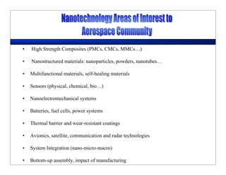
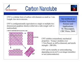
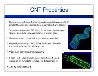
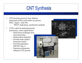
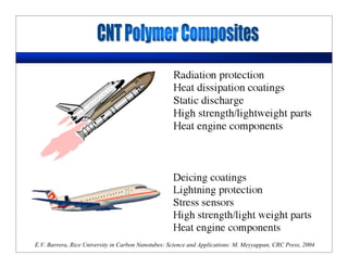
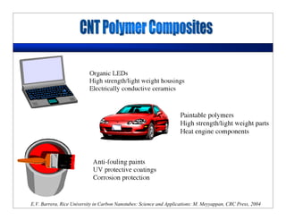
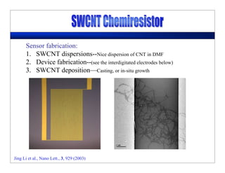
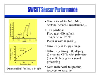
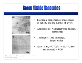
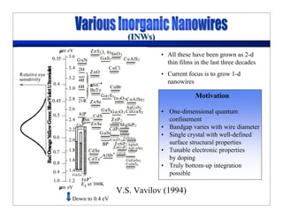
NATO LECTURES
M. Meyyappan
Nanotechnology in Aerospace Applications
Abstract
The aerospace applications for nanotechnology include high strength, low weight
composites, improved electronics and displays with low power consumption, variety of
physical sensors, multifunctional materials with embedded sensors, large surface area
materials and novel filters and membranes for air purification, nanomaterials in tires
and brakes and numerous others. This lecture will introduce nanomaterials particularly
carbon nanotubes, and discuss their properties. The status of composite preparation –
polymer matrix, ceramic matrix and metal matrix – will be presented. Examples of
current developments in the above application areas, particularly physical sensors,
actuators, nanoelectromechanical systems etc. will be presented to show what the
aerospace industry can expect from the field of nanotechnology.
Of all the nanoscale materials, carbon nanotubes (CNTs) have received the most attention
across the world. These are configurationally equivalent to a two-dimensional graphene
sheet rolled up into a tubular structure. With only one wall in the cylinder, the structure
is called a single-walled carbon nanotube (SWCNT). The structure that looks like a
concentric set of cylinders with a constant interlayer separation of 0.34 A is called a
multiwalled carbon nanotube (MWCNT).
The CNT’s structure is characterized by a chiral vector (m, n). When m-n/3 is an integer,
the resulting structure is metallic; otherwise, it is a semiconducting nanotube. This is a
very unique electronic property that has excited the physics and device community
RTO-EN-AVT-129bis 7 - 1
Meyyappan, M. (2007) Nanotechnology in Aerospace Applications. In Nanotechnology Aerospace Applications – 2006 (pp. 7-1 – 7-2).
Educational Notes RTO-EN-AVT-129bis, Paper 7. Neuilly-sur-Seine, France: RTO. Available from: http://www.rto.nato.int/abstracts.asp.
Click here to view PowerPoint presentation; Press Esc to exit
Report Documentation Page
Form Approved
OMB No. 0704-0188
Public reporting burden for the collection of information is estimated to average 1 hour per response, including the time for reviewing instructions, searching existing data sources, gathering and
maintaining the data needed, and completing and reviewing the collection of information. Send comments regarding this burden estimate or any other aspect of this collection of information,
including suggestions for reducing this burden, to Washington Headquarters Services, Directorate for Information Operations and Reports, 1215 Jefferson Davis Highway, Suite 1204, Arlington
VA 22202-4302. Respondents should be aware that notwithstanding any other provision of law, no person shall be subject to a penalty for failing to comply with a collection of information if it
does not display a currently valid OMB control number.
1. REPORT DATE
01 MAR 2007
2. REPORT TYPE
N/A
3. DATES COVERED
-
4. TITLE AND SUBTITLE
Nanotechnology in Aerospace Applications
5a. CONTRACT NUMBER
5b. GRANT NUMBER
5c. PROGRAM ELEMENT NUMBER
6. AUTHOR(S) 5d. PROJECT NUMBER
5e. TASK NUMBER
5f. WORK UNIT NUMBER
7. PERFORMING ORGANIZATION NAME(S) AND ADDRESS(ES)
MM Associates Mail stop 229-3 Bldg 229, Room 214 Moffett Field, CA
94035 UNITED STATES
8. PERFORMING ORGANIZATION
REPORT NUMBER
9. SPONSORING/MONITORING AGENCY NAME(S) AND ADDRESS(ES) 10. SPONSOR/MONITOR’S ACRONYM(S)
11. SPONSOR/MONITOR’S REPORT
NUMBER(S)
12. DISTRIBUTION/AVAILABILITY STATEMENT
Approved for public release, distribution unlimited
13. SUPPLEMENTARY NOTES
See also ADM002060., The original document contains color images.
14. ABSTRACT
15. SUBJECT TERMS
16. SECURITY CLASSIFICATION OF: 17. LIMITATION OF
ABSTRACT
UU
18. NUMBER
OF PAGES
37
19a. NAME OF
RESPONSIBLE PERSON
a. REPORT
unclassified
b. ABSTRACT
unclassified
c. THIS PAGE
unclassified
Standard Form 298 (Rev. 8-98)
Prescribed by ANSI Std Z39-18
leading to numerous possibilities in nanoelectronics. CNTs also exhibit extraordinary
mechanical properties. The Young’s modulus is over 1 TPa and the tensile strength is
about 200 GPa. The thermal conductivity can be as high as 3000 W/mK. With an ideal
aspect ratio, small tip radius of curvature and good emission properties, CNTs also have
proved to be excellent candidates for field emission. CNTs can be chemically
functionalized, i.e. it is possible to attach a variety of atomic and molecular groups to the
ends of sidewalls of the nanotubes.
The impressive properties alluded above have led to investigations of various
applications. The most important aerospace application is high strength, low weight
composites. Investigation of metal and ceramic matrix composites with CNTs as a
constituent materials is in its infancy. A status update will be provided. CNTs have been
shown to provide desirable electrical properties for polymer matrix composites. In many
cases, the current problem is the inability to disperse the nanotubes homogeneously
across the host matrix.
Other applications for CNTs include electronic components, logic and memory chips,
sensors, catalyst support, adsorption media, actuators, etc. All early works in
nanoelectronics use CNTs as a conducting channel in an otherwise silicon CMOS
configuration. This approach may not really have a future as the use of CNTs, while
inherently not solving any of the serious problems of CMOS downscaling (such as
lithography, heat dissipation, etc.), it doesn’t show an order of magnitude performance
improvement either. The critical issue now is to develop alternative architectures in
addition to novel materials. In contrast, the opportunities for CNTs in sensors – both
physical and chemical sensors – are better and near-term.
The opportunities for aerospace industry are through thermal barrier and wear resistant
coatings, sensors that can perform at high temperature and other physical and chemical
sensors, sensors that can perform safety inspection cost effectively, quickly, and
efficiently than the present procedures, composites, wear resistant tires, improved
avionics, satellite, communication and radar technologies.
Nanotechnology in Aerospace Applications
7 - 2 RTO-EN-AVT-129bis
M. Meyyappan
• High Strength Composites (PMCs, CMCs, MMCs…)
• Nanostructured materials: nanoparticles, powders, nanotubes…
• Multifunctional materials, self-healing materials
• Sensors (physical, chemical, bio…)
• Nanoelectromechanical systems
• Batteries, fuel cells, power systems
• Thermal barrier and wear-resistant coatings
• Avionics, satellite, communication and radar technologies
• System Integration (nano-micro-macro)
• Bottom-up assembly, impact of manufacturing
• Processing them into various matrices follow earlier composite
developments such as
- Polymer compounding
- Producing filled polymers
- Assembly of laminate composites
- Polymerizing rigid rod polymers
-
-
• Purpose
- Replace existing materials where properties can be superior
- Applications where traditionally composites were not a
candidate
• Nanotechnology provides new opportunities for radical changes
in composite functionality
• Major benefit is to reach percolation threshold at low volumes
(< 1%) when mixing nanoparticles in a host matrix
• Functionalities can be added when we control the orientation
of the nanoscale reinforcement.
• This always implies “structure +” since in most cases the major
function of a structure is to carry load or provide shape.
Additional functions can be:
• Actuation controlling position, shape or load
• Electrical either insulate or conduct
• Thermal either insulate or conduct
• Health monitor, control
• Stealth managing electromagnetic or visible signature
• Self-healing repair localized damage
• Sensing physical, chemical variables NRC Report, 2003
• Building in additional functionalities into load-bearing structures
is one key example:
- Sensing function
* Strain
* Pressure
* Temperature
* Chemical change
* Contaminant presence
• Miniaturized sensors can be embedded in a distributed fashion to
add “smartness” or multifunctionality. This approach is ‘pre-nano’
era.
• Nanotechnology, in contrast, is expected to help in assembling
materials with such functional capabilities
• Possible, in principle, to design any number of composites with multiple levels
of functionality (3, 4, 5…) by using both multifunctional matrices and
multifunctional reinforcement additives
- Add a capsule into the matrix that contains a nanomaterial sensitive to
thermal, mechanical, electrical stress; when this breaks, would indicate the
area of damage
- Another capsule can contain a healant
- Microcellular structural foam in the matrix may be radar-absorbing,
conducting or light-emitting
- Photovoltaic military uniform also containing Kevlar for protection
generate power during sunlight for charging the batteries of
various devices in the soldier-gear
NRC Report, 2003
• Carbon nanotubes, nanofibers
• Polymer clay nanocomposites
• Polymer cross-linked aerogels
• Biomimetic hybrids
Expectations:
- ‘Designer’ properties, programmable materials
- High strength, low weight
- Low failure rates
- Reduced life cycle costs
‘Self-healing plastic’ by Prof. Scott White (U. of Illinois)
Nature (Feb. 15, 2001)
• Plastic components break because of mechanical or thermal
fatigue. Small cracks ⇒ large cracks ⇒ catastrophic failure.
‘Self-healing’ is a way of repairing these cracks without human
intervention.
• Self-healing plastics have small capsules that release a healing
agent when a crack forms. The agent travels to the crack
through capillaries similar to blood flow to a wound.
• Polymerization is initiated when the agent comes into contact
with a catalyst embedded in the plastic. The chemical reaction
forms a polymer to repair the broken edges of the plastic. New
bond is complete in an hour at room temperature.
• Plasma processing
- Both thermal (plasma arc, plasma torch, plasma spray) and
low temperature (cold) plasma are used
• Chemical Vapor Deposition
- Either on a substrate or in the gas phase (for bulk production)
- Metallic oxides and carbides
• Electrodeposition
• Sol-gel processing
• Ball mill or grinding (old fashioned top-down approach)
Key Issue: AgglomorationKey Issue: Agglomoration
Tremendous increase in surface-to-volume ratio
• Increase in solubility
• Increase in reactivity
• Possible increase in hardness (ex: titanium nitride)
Application range is wide as seen in the next two tables.
MARKET PARTICLES REQUIRED NANOTECHNOLOGY ADVANTAGES
Polishing Slurries Aluminum Oxide Faster rate of surface removal reduces
operating costs
Cerium Oxide Less material required due to small size of
particles
Tin Oxide Better finishing due to finer particles
Capacitors Barium Titanate Less material required for a given level of
capacitance
Tantalum High capacitance due to reduction in layer
thickness and increased surface area resulting
from smaller particle size
Alumina Thinner layers possible, thus significant potential
for device miniaturization
Pigments Iron Oxide Lower material costs, as opacity is obtained with
smaller particles
Zirconium Silicate Better physical-optical properties due to
Titanium Dioxide enhanced control over particles
Dopants Wide variety of materials Improved compositional uniformity
required depending on Reduction in processing temperature reduces
application operating and capital costs
Source: Wilson et al 2002
MARKET PARTICLES REQUIRED NANOTECHNOLOGY ADVANTAGES
Structural Ceramics Aluminium Oxide Improved mechanical properties
Aluminium Titanate Reduced production costs due to lower
sintering temperatures
Zirconium Oxide
Catalysts Titanium Dioxide Increased activity due to smaller particle
size
Cerium Oxide Increased wear resistance
Alumina
Hard Coatings Tungsten Carbide Thin coatings reduce the amount of
material required
Alumina
Conductive Inks Silver Increased conductivity reduces
consumption of valuable metals
Tungsten Lower processing temperatures
Nickel Allows electron lithography
Source: Wilson et al 2002
CNT is a tubular form of carbon with diameter as small as 1 nm.
Length: few nm to microns.
CNT is configurationally equivalent to a single or multiple two
dimensional graphene sheet(s) rolled into a tube (single wall vs.
multiwalled).
CNT exhibits extraordinary mechanical
properties: Young’s modulus over
1 Tera Pascal, as stiff as diamond, and tensile
strength ~ 200 GPa.
CNT can be metallic or semiconducting,
depending on (m-n)/3 is an integer (metallic)
or not (semiconductor).
See textbook on
Carbon Nanotubes:
Science and
Applications,
M. Meyyappan,
CRC Press, 2004.
• The strongest and most flexible molecular material because of C-C
covalent bonding and seamless hexagonal network architecture
• Strength to weight ratio 500 time > for Al, steel, titanium; one
order of magnitude improvement over graphite/epoxy
• Maximum strain ~10% much higher than any material
• Thermal conductivity ~ 3000 W/mK in the axial direction
with small values in the radial direction
• Very high current carrying capacity
• Excellent field emitter; high aspect ratio and small
tip radius of curvature are ideal for field emission
• Can be functionalized
• CNT has been grown by laser ablation
(pioneered at Rice) and carbon arc process
(NEC, Japan) - early 90s.
- SWNT, high purity, purification methods
• CVD is ideal for patterned growth
(electronics, sensor applications)
- Well known technique from
microelectronics
- Hydrocarbon feedstock
- Growth needs catalyst
(transition metal)
- Growth temperature
500-950° deg. C.
- Numerous parameters
influence CNT growth
- Surface masked by a 400 mesh TEM grid
- Methane, 900° C, 10 nm Al/1.0 nm Fe
Delzeit et al., Chem. Phys. Lett.,
348, 368 (2001)
- Surface masked by a 400 mesh TEM grid;
20 nm Al/ 10 nm Fe; 10 minutes
Grown using ethylene at 750o C
Delzeit et al., J. Phys. Chem. B, 106, 5629 (2002)
• Certain applications such as nanoelectrodes, biosensors would
ideally require individual, freestanding, vertical (as opposed to
towers or spaghetti-like) nanostructures
• The high electric field within the sheath near the substrate in a plasma
reactor helps to grow such vertical
structures
• dc, rf, microwave, inductive
plasmas (with a biased substrate)
have been used in PECVD of
such nanostructures
Cassell et al., Nanotechnology, 15 (1), 2004
• Needed for composites, hydrogen storage, other applications
which need bulk material
• Floating catalysts (instead of supported catalysts)
• Carbon source (CO, hydrocarbons)
• Floating catalyst source (Iron pentacarbonyl, ferrocene…)
• Typically, a carrier gas picks up the catalyst source and goes
through first stage furnace (~200° C)
• Precursor injected directly into the 2nd stage furnace
• Decomposition of catalyst source, source gas pysolysis, catalyzed
reactions all occur in the 2nd stage
• Products: Nanotubes, catalyst particles, impurities
• Carbon nanotubes viewed as the “ultimate” nanofibers ever made
• Carbon fibers have been already used as reinforcement in high strength, light
weight, high performace composites:
- Expensive tennis rackets, air-craft body parts…
• Nanotubes are expected to be even better reinforcement
- C-C covalent bonds are one of the strongest in nature
- Young’s modulus ~ 1 TPa ⇒ the in-plane value for defect-free graphite
• Problems
- Creating good interface between CNTs and polymer matrix necessary
for effective load transfer
CNTs are atomically smooth; h/d ~ same as for polymer chains
CNTs are largely in aggregates ⇒ behave differently from individuals
• Solutions
- Breakup aggregates, disperse or cross-link to avoid slippage
- Chemical modification of the surface to obtain strong interface with
surrounding polymer chains
WHY?
• Polymer matrix composites
- Nanotube dispersion
- Untangling
- Alignment
- Bonding
- Molecular Distribution
- Retention of neat-CNT properties
• Metal and Ceramic Matrix Composites
- High temperature stability
- Reactivity
- Suitable processing techniques
- Choice of chemistries to provide stabilization and bonding
to the matrix.
• High aspect ratio allows percolation at lower compositions than spherical fillers
(less than 1% by weight)
• Neat polymer properties such as elongation to failure and optical transparency
are not decreased.
• ESD Materials: Surface resistivity should be 1012 - 105 Ω/sq
- Carpeting, floor mats, wrist straps, electronics packaging
• EMI Applications: Resistivity should be < 105 Ω/sq
- Cellular phone parts
- Frequency shielding coatings for electronics
• High Conducting Materials: Weight saving replacement for metals
- Automotive industry: body panels, bumpers (ease of painting without a
conducting primer)
- Interconnects in various systems where weight saving is critical
E.V. Barrera, Rice University in Carbon Nanotubes: Science and Applications: M. Meyyappan, CRC Press, 2004
• More & more components are packaged in smaller spaces where electromagnetic
interference can become a problem
- Ex: Digital electronics coupled with high power transmitters as in many
microwave systems or even cellular phone systems
• Growing need for thin coatings which can help isolate critical components from
other components of the system and external world
• Carbon nanofibers have been tested for EMI shielding; nanotubes have potential
as well
- Act as absorber/scatterer of radar and microwave radiation
- High aspect ratio is advantageous
- Efficiency is boosted by small diameter. Large d will have material too
deep inside to affect the process. At sub-100 nm, all of the material
participate in the absorption
- Carbon fibers and nanotubes (< 2 g/cc) have better specific conductivity
than metal fillers, sometimes used as radar absorbing materials.
Single Wall Carbon Nanotube
• Every atom in a single-walled nanotube (SWNT) is on
the surface and exposed to environment
• Charge transfer or small changes in the charge-
environment of a nanotube can cause drastic changes
to its electrical properties
Sensor fabrication:
1. SWCNT dispersions--Nice dispersion of CNT in DMF
2. Device fabrication--(see the interdigitated electrodes below)
3. SWCNT deposition—Casting, or in-situ growth
Jing Li et al., Nano Lett., 3, 929 (2003)
Detection limit for NO2 is 44 ppb.
• Sensor tested for NO2, NH3,
acetone, benzene, nitrotoulene…
• Test condition:
Flow rate: 400 ml/min
Temperature: 23 oC
Purge & carrier gas: N2
• Sensitivity in the ppb range
• Selectivity through (1) doping,
(2) coating CNTs with polymers,
(3) multiplexing with signal
processing
• Need more work to speedup
recovery to baseline
• Electronic properties are independent
of helicity and the number of layers
• Applications: Nanoelectronic devices,
composites
• Techniques: Arc discharge,
laser ablation
• Also: B2O3 + C (CNT) + N2 → 2 BN
(nanotubes) + 3 CO
Motivation
• One-dimensional quantum
confinement
• Bandgap varies with wire diameter
• Single crystal with well-defined
surface structural properties
• Tunable electronic properties
by doping
• Truly bottom-up integration
possible
V.S. Vavilov (1994)
Down to 0.4 eV
• All these have been grown as 2-d
thin films in the last three decades
• Current focus is to grow 1-d
nanowires
(INWs)(INWs)
(0001)
Low dimensional systems
nanowires
Conduction electron density of
state
Seebeck coefficient
Structural constraints
thermal conductivity
0
5
10
15
20
25
0 10 20 30
wire width (nm)
figureofmerit,ZT
n-doped
p-doped
*PRL 47, 16631 (1993)
Electrical interconnectsCopper, Tungsten
Photonics (Q-switch, blue-green laser diode, blue-UV
photodetector)
Zinc Selenide
Electronics, optoelectronicsIndium Phosphide
InsulatorBoron Nitride
High temperature electronics, UV detectors and lasers,
automotive electronics and sensors
Wide Bandgap Nitrides (GaN)
Field emission deviceCopper Oxide
UV laser, field emission device, chemical sensorZinc Oxide
Transparent conductive film in display electrodes, solar
cells, organic light emitting diodes
Indium Tin Oxide
Chemical sensors, biosensorsIndium Oxide
Chemical sensorsTin Oxide
Electronics, IR detectorsGermanium
Electronics, sensorsSilicon
APPLICATIONMATERIAL
• Nanotechnology is an enabling technology that will impact the aerospace
sector through composites, advances in electronics, sensors,
instrumentation, materials, manufacturing processes, etc.
• The field is interdisciplinary but everything starts with material science.
Challenges include:
- Novel synthesis techniques
- Characterization of nanoscale properties
- Large scale production of materials
- Application development
• Opportunities and rewards are great and hence, there is a tremendous
worldwide interest

Nano tech applications in aerospace

  • 1.
    NATO LECTURES M. Meyyappan Nanotechnologyin Aerospace Applications Abstract The aerospace applications for nanotechnology include high strength, low weight composites, improved electronics and displays with low power consumption, variety of physical sensors, multifunctional materials with embedded sensors, large surface area materials and novel filters and membranes for air purification, nanomaterials in tires and brakes and numerous others. This lecture will introduce nanomaterials particularly carbon nanotubes, and discuss their properties. The status of composite preparation – polymer matrix, ceramic matrix and metal matrix – will be presented. Examples of current developments in the above application areas, particularly physical sensors, actuators, nanoelectromechanical systems etc. will be presented to show what the aerospace industry can expect from the field of nanotechnology. Of all the nanoscale materials, carbon nanotubes (CNTs) have received the most attention across the world. These are configurationally equivalent to a two-dimensional graphene sheet rolled up into a tubular structure. With only one wall in the cylinder, the structure is called a single-walled carbon nanotube (SWCNT). The structure that looks like a concentric set of cylinders with a constant interlayer separation of 0.34 A is called a multiwalled carbon nanotube (MWCNT). The CNT’s structure is characterized by a chiral vector (m, n). When m-n/3 is an integer, the resulting structure is metallic; otherwise, it is a semiconducting nanotube. This is a very unique electronic property that has excited the physics and device community RTO-EN-AVT-129bis 7 - 1 Meyyappan, M. (2007) Nanotechnology in Aerospace Applications. In Nanotechnology Aerospace Applications – 2006 (pp. 7-1 – 7-2). Educational Notes RTO-EN-AVT-129bis, Paper 7. Neuilly-sur-Seine, France: RTO. Available from: http://www.rto.nato.int/abstracts.asp. Click here to view PowerPoint presentation; Press Esc to exit
  • 2.
    Report Documentation Page FormApproved OMB No. 0704-0188 Public reporting burden for the collection of information is estimated to average 1 hour per response, including the time for reviewing instructions, searching existing data sources, gathering and maintaining the data needed, and completing and reviewing the collection of information. Send comments regarding this burden estimate or any other aspect of this collection of information, including suggestions for reducing this burden, to Washington Headquarters Services, Directorate for Information Operations and Reports, 1215 Jefferson Davis Highway, Suite 1204, Arlington VA 22202-4302. Respondents should be aware that notwithstanding any other provision of law, no person shall be subject to a penalty for failing to comply with a collection of information if it does not display a currently valid OMB control number. 1. REPORT DATE 01 MAR 2007 2. REPORT TYPE N/A 3. DATES COVERED - 4. TITLE AND SUBTITLE Nanotechnology in Aerospace Applications 5a. CONTRACT NUMBER 5b. GRANT NUMBER 5c. PROGRAM ELEMENT NUMBER 6. AUTHOR(S) 5d. PROJECT NUMBER 5e. TASK NUMBER 5f. WORK UNIT NUMBER 7. PERFORMING ORGANIZATION NAME(S) AND ADDRESS(ES) MM Associates Mail stop 229-3 Bldg 229, Room 214 Moffett Field, CA 94035 UNITED STATES 8. PERFORMING ORGANIZATION REPORT NUMBER 9. SPONSORING/MONITORING AGENCY NAME(S) AND ADDRESS(ES) 10. SPONSOR/MONITOR’S ACRONYM(S) 11. SPONSOR/MONITOR’S REPORT NUMBER(S) 12. DISTRIBUTION/AVAILABILITY STATEMENT Approved for public release, distribution unlimited 13. SUPPLEMENTARY NOTES See also ADM002060., The original document contains color images. 14. ABSTRACT 15. SUBJECT TERMS 16. SECURITY CLASSIFICATION OF: 17. LIMITATION OF ABSTRACT UU 18. NUMBER OF PAGES 37 19a. NAME OF RESPONSIBLE PERSON a. REPORT unclassified b. ABSTRACT unclassified c. THIS PAGE unclassified Standard Form 298 (Rev. 8-98) Prescribed by ANSI Std Z39-18
  • 3.
    leading to numerouspossibilities in nanoelectronics. CNTs also exhibit extraordinary mechanical properties. The Young’s modulus is over 1 TPa and the tensile strength is about 200 GPa. The thermal conductivity can be as high as 3000 W/mK. With an ideal aspect ratio, small tip radius of curvature and good emission properties, CNTs also have proved to be excellent candidates for field emission. CNTs can be chemically functionalized, i.e. it is possible to attach a variety of atomic and molecular groups to the ends of sidewalls of the nanotubes. The impressive properties alluded above have led to investigations of various applications. The most important aerospace application is high strength, low weight composites. Investigation of metal and ceramic matrix composites with CNTs as a constituent materials is in its infancy. A status update will be provided. CNTs have been shown to provide desirable electrical properties for polymer matrix composites. In many cases, the current problem is the inability to disperse the nanotubes homogeneously across the host matrix. Other applications for CNTs include electronic components, logic and memory chips, sensors, catalyst support, adsorption media, actuators, etc. All early works in nanoelectronics use CNTs as a conducting channel in an otherwise silicon CMOS configuration. This approach may not really have a future as the use of CNTs, while inherently not solving any of the serious problems of CMOS downscaling (such as lithography, heat dissipation, etc.), it doesn’t show an order of magnitude performance improvement either. The critical issue now is to develop alternative architectures in addition to novel materials. In contrast, the opportunities for CNTs in sensors – both physical and chemical sensors – are better and near-term. The opportunities for aerospace industry are through thermal barrier and wear resistant coatings, sensors that can perform at high temperature and other physical and chemical sensors, sensors that can perform safety inspection cost effectively, quickly, and efficiently than the present procedures, composites, wear resistant tires, improved avionics, satellite, communication and radar technologies. Nanotechnology in Aerospace Applications 7 - 2 RTO-EN-AVT-129bis
  • 4.
  • 5.
    • High StrengthComposites (PMCs, CMCs, MMCs…) • Nanostructured materials: nanoparticles, powders, nanotubes… • Multifunctional materials, self-healing materials • Sensors (physical, chemical, bio…) • Nanoelectromechanical systems • Batteries, fuel cells, power systems • Thermal barrier and wear-resistant coatings • Avionics, satellite, communication and radar technologies • System Integration (nano-micro-macro) • Bottom-up assembly, impact of manufacturing
  • 6.
    • Processing theminto various matrices follow earlier composite developments such as - Polymer compounding - Producing filled polymers - Assembly of laminate composites - Polymerizing rigid rod polymers - - • Purpose - Replace existing materials where properties can be superior - Applications where traditionally composites were not a candidate
  • 7.
    • Nanotechnology providesnew opportunities for radical changes in composite functionality • Major benefit is to reach percolation threshold at low volumes (< 1%) when mixing nanoparticles in a host matrix • Functionalities can be added when we control the orientation of the nanoscale reinforcement.
  • 8.
    • This alwaysimplies “structure +” since in most cases the major function of a structure is to carry load or provide shape. Additional functions can be: • Actuation controlling position, shape or load • Electrical either insulate or conduct • Thermal either insulate or conduct • Health monitor, control • Stealth managing electromagnetic or visible signature • Self-healing repair localized damage • Sensing physical, chemical variables NRC Report, 2003
  • 9.
    • Building inadditional functionalities into load-bearing structures is one key example: - Sensing function * Strain * Pressure * Temperature * Chemical change * Contaminant presence • Miniaturized sensors can be embedded in a distributed fashion to add “smartness” or multifunctionality. This approach is ‘pre-nano’ era. • Nanotechnology, in contrast, is expected to help in assembling materials with such functional capabilities
  • 10.
    • Possible, inprinciple, to design any number of composites with multiple levels of functionality (3, 4, 5…) by using both multifunctional matrices and multifunctional reinforcement additives - Add a capsule into the matrix that contains a nanomaterial sensitive to thermal, mechanical, electrical stress; when this breaks, would indicate the area of damage - Another capsule can contain a healant - Microcellular structural foam in the matrix may be radar-absorbing, conducting or light-emitting - Photovoltaic military uniform also containing Kevlar for protection generate power during sunlight for charging the batteries of various devices in the soldier-gear NRC Report, 2003
  • 11.
    • Carbon nanotubes,nanofibers • Polymer clay nanocomposites • Polymer cross-linked aerogels • Biomimetic hybrids Expectations: - ‘Designer’ properties, programmable materials - High strength, low weight - Low failure rates - Reduced life cycle costs
  • 12.
    ‘Self-healing plastic’ byProf. Scott White (U. of Illinois) Nature (Feb. 15, 2001) • Plastic components break because of mechanical or thermal fatigue. Small cracks ⇒ large cracks ⇒ catastrophic failure. ‘Self-healing’ is a way of repairing these cracks without human intervention. • Self-healing plastics have small capsules that release a healing agent when a crack forms. The agent travels to the crack through capillaries similar to blood flow to a wound. • Polymerization is initiated when the agent comes into contact with a catalyst embedded in the plastic. The chemical reaction forms a polymer to repair the broken edges of the plastic. New bond is complete in an hour at room temperature.
  • 13.
    • Plasma processing -Both thermal (plasma arc, plasma torch, plasma spray) and low temperature (cold) plasma are used • Chemical Vapor Deposition - Either on a substrate or in the gas phase (for bulk production) - Metallic oxides and carbides • Electrodeposition • Sol-gel processing • Ball mill or grinding (old fashioned top-down approach) Key Issue: AgglomorationKey Issue: Agglomoration
  • 14.
    Tremendous increase insurface-to-volume ratio • Increase in solubility • Increase in reactivity • Possible increase in hardness (ex: titanium nitride) Application range is wide as seen in the next two tables.
  • 15.
    MARKET PARTICLES REQUIREDNANOTECHNOLOGY ADVANTAGES Polishing Slurries Aluminum Oxide Faster rate of surface removal reduces operating costs Cerium Oxide Less material required due to small size of particles Tin Oxide Better finishing due to finer particles Capacitors Barium Titanate Less material required for a given level of capacitance Tantalum High capacitance due to reduction in layer thickness and increased surface area resulting from smaller particle size Alumina Thinner layers possible, thus significant potential for device miniaturization Pigments Iron Oxide Lower material costs, as opacity is obtained with smaller particles Zirconium Silicate Better physical-optical properties due to Titanium Dioxide enhanced control over particles Dopants Wide variety of materials Improved compositional uniformity required depending on Reduction in processing temperature reduces application operating and capital costs Source: Wilson et al 2002
  • 16.
    MARKET PARTICLES REQUIREDNANOTECHNOLOGY ADVANTAGES Structural Ceramics Aluminium Oxide Improved mechanical properties Aluminium Titanate Reduced production costs due to lower sintering temperatures Zirconium Oxide Catalysts Titanium Dioxide Increased activity due to smaller particle size Cerium Oxide Increased wear resistance Alumina Hard Coatings Tungsten Carbide Thin coatings reduce the amount of material required Alumina Conductive Inks Silver Increased conductivity reduces consumption of valuable metals Tungsten Lower processing temperatures Nickel Allows electron lithography Source: Wilson et al 2002
  • 17.
    CNT is atubular form of carbon with diameter as small as 1 nm. Length: few nm to microns. CNT is configurationally equivalent to a single or multiple two dimensional graphene sheet(s) rolled into a tube (single wall vs. multiwalled). CNT exhibits extraordinary mechanical properties: Young’s modulus over 1 Tera Pascal, as stiff as diamond, and tensile strength ~ 200 GPa. CNT can be metallic or semiconducting, depending on (m-n)/3 is an integer (metallic) or not (semiconductor). See textbook on Carbon Nanotubes: Science and Applications, M. Meyyappan, CRC Press, 2004.
  • 18.
    • The strongestand most flexible molecular material because of C-C covalent bonding and seamless hexagonal network architecture • Strength to weight ratio 500 time > for Al, steel, titanium; one order of magnitude improvement over graphite/epoxy • Maximum strain ~10% much higher than any material • Thermal conductivity ~ 3000 W/mK in the axial direction with small values in the radial direction • Very high current carrying capacity • Excellent field emitter; high aspect ratio and small tip radius of curvature are ideal for field emission • Can be functionalized
  • 19.
    • CNT hasbeen grown by laser ablation (pioneered at Rice) and carbon arc process (NEC, Japan) - early 90s. - SWNT, high purity, purification methods • CVD is ideal for patterned growth (electronics, sensor applications) - Well known technique from microelectronics - Hydrocarbon feedstock - Growth needs catalyst (transition metal) - Growth temperature 500-950° deg. C. - Numerous parameters influence CNT growth
  • 20.
    - Surface maskedby a 400 mesh TEM grid - Methane, 900° C, 10 nm Al/1.0 nm Fe Delzeit et al., Chem. Phys. Lett., 348, 368 (2001)
  • 21.
    - Surface maskedby a 400 mesh TEM grid; 20 nm Al/ 10 nm Fe; 10 minutes Grown using ethylene at 750o C Delzeit et al., J. Phys. Chem. B, 106, 5629 (2002)
  • 22.
    • Certain applicationssuch as nanoelectrodes, biosensors would ideally require individual, freestanding, vertical (as opposed to towers or spaghetti-like) nanostructures • The high electric field within the sheath near the substrate in a plasma reactor helps to grow such vertical structures • dc, rf, microwave, inductive plasmas (with a biased substrate) have been used in PECVD of such nanostructures Cassell et al., Nanotechnology, 15 (1), 2004
  • 23.
    • Needed forcomposites, hydrogen storage, other applications which need bulk material • Floating catalysts (instead of supported catalysts) • Carbon source (CO, hydrocarbons) • Floating catalyst source (Iron pentacarbonyl, ferrocene…) • Typically, a carrier gas picks up the catalyst source and goes through first stage furnace (~200° C) • Precursor injected directly into the 2nd stage furnace • Decomposition of catalyst source, source gas pysolysis, catalyzed reactions all occur in the 2nd stage • Products: Nanotubes, catalyst particles, impurities
  • 24.
    • Carbon nanotubesviewed as the “ultimate” nanofibers ever made • Carbon fibers have been already used as reinforcement in high strength, light weight, high performace composites: - Expensive tennis rackets, air-craft body parts… • Nanotubes are expected to be even better reinforcement - C-C covalent bonds are one of the strongest in nature - Young’s modulus ~ 1 TPa ⇒ the in-plane value for defect-free graphite • Problems - Creating good interface between CNTs and polymer matrix necessary for effective load transfer CNTs are atomically smooth; h/d ~ same as for polymer chains CNTs are largely in aggregates ⇒ behave differently from individuals • Solutions - Breakup aggregates, disperse or cross-link to avoid slippage - Chemical modification of the surface to obtain strong interface with surrounding polymer chains WHY?
  • 25.
    • Polymer matrixcomposites - Nanotube dispersion - Untangling - Alignment - Bonding - Molecular Distribution - Retention of neat-CNT properties • Metal and Ceramic Matrix Composites - High temperature stability - Reactivity - Suitable processing techniques - Choice of chemistries to provide stabilization and bonding to the matrix.
  • 26.
    • High aspectratio allows percolation at lower compositions than spherical fillers (less than 1% by weight) • Neat polymer properties such as elongation to failure and optical transparency are not decreased. • ESD Materials: Surface resistivity should be 1012 - 105 Ω/sq - Carpeting, floor mats, wrist straps, electronics packaging • EMI Applications: Resistivity should be < 105 Ω/sq - Cellular phone parts - Frequency shielding coatings for electronics • High Conducting Materials: Weight saving replacement for metals - Automotive industry: body panels, bumpers (ease of painting without a conducting primer) - Interconnects in various systems where weight saving is critical
  • 27.
    E.V. Barrera, RiceUniversity in Carbon Nanotubes: Science and Applications: M. Meyyappan, CRC Press, 2004
  • 28.
    E.V. Barrera, RiceUniversity in Carbon Nanotubes: Science and Applications: M. Meyyappan, CRC Press, 2004
  • 29.
    • More &more components are packaged in smaller spaces where electromagnetic interference can become a problem - Ex: Digital electronics coupled with high power transmitters as in many microwave systems or even cellular phone systems • Growing need for thin coatings which can help isolate critical components from other components of the system and external world • Carbon nanofibers have been tested for EMI shielding; nanotubes have potential as well - Act as absorber/scatterer of radar and microwave radiation - High aspect ratio is advantageous - Efficiency is boosted by small diameter. Large d will have material too deep inside to affect the process. At sub-100 nm, all of the material participate in the absorption - Carbon fibers and nanotubes (< 2 g/cc) have better specific conductivity than metal fillers, sometimes used as radar absorbing materials.
  • 30.
    Single Wall CarbonNanotube • Every atom in a single-walled nanotube (SWNT) is on the surface and exposed to environment • Charge transfer or small changes in the charge- environment of a nanotube can cause drastic changes to its electrical properties
  • 31.
    Sensor fabrication: 1. SWCNTdispersions--Nice dispersion of CNT in DMF 2. Device fabrication--(see the interdigitated electrodes below) 3. SWCNT deposition—Casting, or in-situ growth Jing Li et al., Nano Lett., 3, 929 (2003)
  • 32.
    Detection limit forNO2 is 44 ppb. • Sensor tested for NO2, NH3, acetone, benzene, nitrotoulene… • Test condition: Flow rate: 400 ml/min Temperature: 23 oC Purge & carrier gas: N2 • Sensitivity in the ppb range • Selectivity through (1) doping, (2) coating CNTs with polymers, (3) multiplexing with signal processing • Need more work to speedup recovery to baseline
  • 33.
    • Electronic propertiesare independent of helicity and the number of layers • Applications: Nanoelectronic devices, composites • Techniques: Arc discharge, laser ablation • Also: B2O3 + C (CNT) + N2 → 2 BN (nanotubes) + 3 CO
  • 34.
    Motivation • One-dimensional quantum confinement •Bandgap varies with wire diameter • Single crystal with well-defined surface structural properties • Tunable electronic properties by doping • Truly bottom-up integration possible V.S. Vavilov (1994) Down to 0.4 eV • All these have been grown as 2-d thin films in the last three decades • Current focus is to grow 1-d nanowires (INWs)(INWs)
  • 35.
  • 36.
    Low dimensional systems nanowires Conductionelectron density of state Seebeck coefficient Structural constraints thermal conductivity 0 5 10 15 20 25 0 10 20 30 wire width (nm) figureofmerit,ZT n-doped p-doped *PRL 47, 16631 (1993)
  • 37.
    Electrical interconnectsCopper, Tungsten Photonics(Q-switch, blue-green laser diode, blue-UV photodetector) Zinc Selenide Electronics, optoelectronicsIndium Phosphide InsulatorBoron Nitride High temperature electronics, UV detectors and lasers, automotive electronics and sensors Wide Bandgap Nitrides (GaN) Field emission deviceCopper Oxide UV laser, field emission device, chemical sensorZinc Oxide Transparent conductive film in display electrodes, solar cells, organic light emitting diodes Indium Tin Oxide Chemical sensors, biosensorsIndium Oxide Chemical sensorsTin Oxide Electronics, IR detectorsGermanium Electronics, sensorsSilicon APPLICATIONMATERIAL
  • 38.
    • Nanotechnology isan enabling technology that will impact the aerospace sector through composites, advances in electronics, sensors, instrumentation, materials, manufacturing processes, etc. • The field is interdisciplinary but everything starts with material science. Challenges include: - Novel synthesis techniques - Characterization of nanoscale properties - Large scale production of materials - Application development • Opportunities and rewards are great and hence, there is a tremendous worldwide interest