Spring 2015
Organic Memories
Dr. Farhad Akbari Boroumand
By:
Atiyeh Koohi Saadi
2/22
Outline
• Electronic Memory
• Types of electronic memory
• Transistor-type polymer memories
– Device structures
– Operating principle
• Nonvolatile memory with graphene
• One Diode-One Resistor Cell Array for Memory
• Photochromic Transduction Layers in Memory
– Light-emitting organic memory
• Conclusion
3/22
Electronic Memory
Electronic storage devices:
• retains retrievable digital data over a time interval
• fast in response
• compact in size
• read and write feasible when connected to a central processing unit
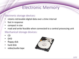
Mechanical storage devices:
• CD
• DVD
• floppy disk
• hard disk
• video/audio tape
4/22
Types of electronic memory
Types of memory
Non-volatile memory
ROM
EPROM WORM
Hybrid
Flash EEPROM FeROM
Volatile memory
(RAM)
DRAM SRAM
5/22
Transistor-type polymer memories
• Application of organic transistors in memories
• Simple fabrication process of OTFTs
• Low cost
• Light weight
• mechanical flexibility of organic materials
6/22
Device structures
• Design features similar to MOSFET
Main component:
1. source (S), drain (D) and gate (G)
2. dielectric layer
3. active semiconductor layer
7/22
Device structures
• Electrodes : Au for polymer-based FETs  ohmic
contact with conjugated polymers
• Dielectric : inorganic or polymeric insulator
• Semiconductor : conjugated molecule or polymer
• Substrate : glass, wafer, or plastic
8/22
Operating principle
• Control over the source–drain current in OFETs via a
third terminal  applications in switches, shift
registers and logic elements  volatile
• An additional voltage, between the gate and the
semiconductor channel to alter the charge
distribution  nonvolatile
Writing : VG = 200V and VD = 0V
Reading : VG =0V and VD =−30V
Erasing : VG =−100V and VD =0V
9/22
Operating principle
10/22
Nonvolatile memory with graphene
• Graphene :
– Transparency
– Conduction properties
– Solution possibility
Multilayer graphene film (MLG) as interlayer
between insulating polyimide (PI) layers
WORM type characteristics
ON/OFF ratio of over 6
10
11/22
Nonvolatile memory with graphene
Fabrication:
12/22
Nonvolatile memory with graphene
80 nm
3 nm
13/22
Nonvolatile memory with graphene
WORM memory type
14/22
One Diode-One Resistor Cell Array for Memory
15/22
Photochromic Transduction Layers in Memory
 utilization of photochromic materials (PCM), as
switching/transduction layers
Closed molecular
Open isomer
•The open isomer is converted to the
closed form via a UV-induced reaction
•The closed structure can be returned to
the open configuration via visible light
excitation
16/22
o Black curve  open isomers
o Gray curves  closed isomers
o red-shift in absorption bands by the identity of the R and R’ moieties
 Minimum barriers from HTM (and ETM) into the PCM in the ON state (closed)
 Maximum barriers from HTM (and ETM) into the PCM in the OFF state (open)
Photochromic Transduction Layers in Memory
17/22
1. ITO anode
2. PEDOT:PSS hole-
injection layer
3. Crosslinked
triphenylamine dimer
(XTPD) derivatives as
hole transport layers
4. XDTE
phototransduction
layer
5. Poly (spirofluorene)
emission and electron
transport layer
6. Ba cathode
7. Al top contact
Light-emitting organic memory
18/22
Light-emitting organic memory
19/22
Conclusion
 polymer memories, an alternative to the conventional
memory technologies due to miniaturizing from micro to
nanoscale
challenges:
switching and transport properties
validation of transport properties
 the exclusion of electrode reactions
Characteristics:
Low cost
low processing temperature
potential for flexible devices
20/22
Organic Memristor
21/22
References
[1]. Qi-Dan Linga, Der-Jang Liawb, Chunxiang Zhuc, Daniel Siu-Hung Chanc,
En-Tang Kanga, Koon-Gee Neoha, “Polymer electronic memories:
Materials, devices and mechanisms” , 2008
[2]. Yongsung Ji, Minhyeok Choe, Byungjin Cho, Sunghoon Song,
Jongwon Yoon, Heung Cho Ko and Takhee Lee, “Organic nonvolatile memory
devices with charge trapping multilayer graphene film” , 2012
[3]. Tae-Wook Kim, David F. Zeigler, Orb Acton, Hin-Lap Yip, Hong Ma, and
Alex K.-Y. Jen, “All-Organic Photopatterned One Diode-One Resistor Cell
Array for Advanced Organic Nonvolatile Memory Applications” , 2012
[4]. R. Clayton Shallcross, Philipp Zacharias, Anne Köhnen, Peter O.Körner,
Eduard Maibach , and Klaus Meerholz, “Photochromic Transduction Layers
in Organic Memory Elements” , 2013
22/22

Organic memories

  • 1.
    Spring 2015 Organic Memories Dr.Farhad Akbari Boroumand By: Atiyeh Koohi Saadi
  • 2.
    2/22 Outline • Electronic Memory •Types of electronic memory • Transistor-type polymer memories – Device structures – Operating principle • Nonvolatile memory with graphene • One Diode-One Resistor Cell Array for Memory • Photochromic Transduction Layers in Memory – Light-emitting organic memory • Conclusion
  • 3.
    3/22 Electronic Memory Electronic storagedevices: • retains retrievable digital data over a time interval • fast in response • compact in size • read and write feasible when connected to a central processing unit Mechanical storage devices: • CD • DVD • floppy disk • hard disk • video/audio tape
  • 4.
    4/22 Types of electronicmemory Types of memory Non-volatile memory ROM EPROM WORM Hybrid Flash EEPROM FeROM Volatile memory (RAM) DRAM SRAM
  • 5.
    5/22 Transistor-type polymer memories •Application of organic transistors in memories • Simple fabrication process of OTFTs • Low cost • Light weight • mechanical flexibility of organic materials
  • 6.
    6/22 Device structures • Designfeatures similar to MOSFET Main component: 1. source (S), drain (D) and gate (G) 2. dielectric layer 3. active semiconductor layer
  • 7.
    7/22 Device structures • Electrodes: Au for polymer-based FETs  ohmic contact with conjugated polymers • Dielectric : inorganic or polymeric insulator • Semiconductor : conjugated molecule or polymer • Substrate : glass, wafer, or plastic
  • 8.
    8/22 Operating principle • Controlover the source–drain current in OFETs via a third terminal  applications in switches, shift registers and logic elements  volatile • An additional voltage, between the gate and the semiconductor channel to alter the charge distribution  nonvolatile Writing : VG = 200V and VD = 0V Reading : VG =0V and VD =−30V Erasing : VG =−100V and VD =0V
  • 9.
  • 10.
    10/22 Nonvolatile memory withgraphene • Graphene : – Transparency – Conduction properties – Solution possibility Multilayer graphene film (MLG) as interlayer between insulating polyimide (PI) layers WORM type characteristics ON/OFF ratio of over 6 10
  • 11.
    11/22 Nonvolatile memory withgraphene Fabrication:
  • 12.
    12/22 Nonvolatile memory withgraphene 80 nm 3 nm
  • 13.
    13/22 Nonvolatile memory withgraphene WORM memory type
  • 14.
    14/22 One Diode-One ResistorCell Array for Memory
  • 15.
    15/22 Photochromic Transduction Layersin Memory  utilization of photochromic materials (PCM), as switching/transduction layers Closed molecular Open isomer •The open isomer is converted to the closed form via a UV-induced reaction •The closed structure can be returned to the open configuration via visible light excitation
  • 16.
    16/22 o Black curve open isomers o Gray curves  closed isomers o red-shift in absorption bands by the identity of the R and R’ moieties  Minimum barriers from HTM (and ETM) into the PCM in the ON state (closed)  Maximum barriers from HTM (and ETM) into the PCM in the OFF state (open) Photochromic Transduction Layers in Memory
  • 17.
    17/22 1. ITO anode 2.PEDOT:PSS hole- injection layer 3. Crosslinked triphenylamine dimer (XTPD) derivatives as hole transport layers 4. XDTE phototransduction layer 5. Poly (spirofluorene) emission and electron transport layer 6. Ba cathode 7. Al top contact Light-emitting organic memory
  • 18.
  • 19.
    19/22 Conclusion  polymer memories,an alternative to the conventional memory technologies due to miniaturizing from micro to nanoscale challenges: switching and transport properties validation of transport properties  the exclusion of electrode reactions Characteristics: Low cost low processing temperature potential for flexible devices
  • 20.
  • 21.
    21/22 References [1]. Qi-Dan Linga,Der-Jang Liawb, Chunxiang Zhuc, Daniel Siu-Hung Chanc, En-Tang Kanga, Koon-Gee Neoha, “Polymer electronic memories: Materials, devices and mechanisms” , 2008 [2]. Yongsung Ji, Minhyeok Choe, Byungjin Cho, Sunghoon Song, Jongwon Yoon, Heung Cho Ko and Takhee Lee, “Organic nonvolatile memory devices with charge trapping multilayer graphene film” , 2012 [3]. Tae-Wook Kim, David F. Zeigler, Orb Acton, Hin-Lap Yip, Hong Ma, and Alex K.-Y. Jen, “All-Organic Photopatterned One Diode-One Resistor Cell Array for Advanced Organic Nonvolatile Memory Applications” , 2012 [4]. R. Clayton Shallcross, Philipp Zacharias, Anne Köhnen, Peter O.Körner, Eduard Maibach , and Klaus Meerholz, “Photochromic Transduction Layers in Organic Memory Elements” , 2013
  • 22.