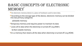
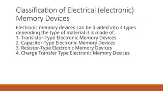
MODULE 2
MATERIALS FOR MEMORY
AND DISPLAY SYSTEMS
BASIC CONCEPTS OF ELECTRONIC
MEMORY
An electronic memory device is a piece of hardware used to store data.
According to the storage type of the device, electronic memory can be divided
into two primary categories
a)Volatile memory:
Temporary memory and requires power to maintain its data
 Loses all its data when the electricity is turned off. (e.g RAM )
b) Non-volatile memory
It is a memory that retains all the data when electricity is turned off. (e.g ROM)
1. Primary/main memory: Primary memory is the internal memory of the computer and can be
directly accessed by the processor.
This is further divided into two parts:-
Random Access Memory (RAM):
 It is a type of volatile memory commonly used in computers.
 RAM allows a computer to quickly access and store information for immediate
use. However, since it requires power to maintain its data, RAM is cleared when
power is turned off, resulting in the loss of any unsaved data
There are two types of RAM:
STATIC RAM (SRAM)
Uses a transistor to store
data
The word “static” refers
that the memory retains its
contents as long as the
power is supplied so that’s
why we can say this is volatile
in nature.
SRAM does not need to be
refreshed periodically .
SRAM is faster but more
DYNAMIC RAM (DRAM)
It is a type of volatile memory that
uses a capacitor to store data
 It is called "dynamic" because it
needs to be constantly refreshed to
maintain the data.
 DRAM is cheaper than other
types of memory and is
commonly used as the main
memory in computers.
However, it is slower than other
types of memory and needs to be
Read-only memory (ROM)
 ROM only allows read-only operations.
It is a non-volatile memory that retains all the data when
electricity is turned off.
It is a type of computer memory used to store permanent
data that cannot be changed.
 Data is written to ROM during manufacturing and cannot
be changed afterward
There are 3 types of ROM: PROM, EPROM and EEPROM
a. PROM-Programmable Read Only
memory
When the data is stored we have no right to change or alter any data to it and is
non-volatile in nature.
In this the data is written by Manufacturer company.
 In general PC’s mainly PROM is used because we don’t have to alter any data
to it .
It contains BIOS of system.
t is used to store data bases other massive data where information has to
be preserved for a long period of time
b. EPROM -Erasable programmable read only memory
EPROM is a memory device whose content can be erased by exposing it to
UV light.
 It allows users to write new data on it after erasing
c. EEPROM- Electrically Erasable PROM
It is known as “the type of ROM which can be erased by electrical charges.
EEPROM can be erased one byte at anytime rather than erasing the entire
chip by ultra
violet rays
2. External/secondary memory:
It is a non-volatile memory which is not directly accessed by CPU.
 It refers to the various storage media on which a computer can
store data and programs.
The Secondary storage media can be fixed or removable.
 Fixed Storage media is an internal storage medium like a
hard disk that is fixed inside the computer.
A storage medium that is portable and can be taken outside the
computer is termed removable storage media. Ex.CD, USB, External
hard disk
Classification of Electrical (electronic)
Memory Devices
Electronic memory devices can be divided into 4 types
depending the type of material it is made of.
1. Transistor-Type Electronic Memory Devices
2. Capacitor-Type Electronic Memory Devices
3. Resistor-Type Electronic Memory Devices
4. Charge Transfer Type Electronic Memory Devices
Transistor-Type Electronic Memory
oTransistors are made from silicon, a semiconductor.
oIt is converted to p-type and n-type semiconductor by doping
trivalent and pentavalent impurities.
oA transistor is a miniature electronic component that can
work either as an amplifier or a switch.
oA computer memory chip consists of billions of transistors;
each transistor is working as a switch, which can be switched
ON or OFF.
oEach transistor can be in two different states and store two
different numbers, ZERO and ONE. Since chip is made of
billions of such transistors and can store billions of Zeros and
Capacitor-Type Electronic Memory
oA capacitor consists of two metal plates which are capable of storing an
electric charge. It is used to store data.
oIt is like a battery that holds data based on energy. If the capacitor is charged,
it holds the binary numeral, “1” and holds “0” when the cell is discharged.
oIf the parallel plates of a capacitor are separated by dielectric layer, charges
dissipate slowly and memory would be volatile.
oOn the other hand, if the medium between the electrodes is ferroelectric in
nature, can maintain permanent electric polarization that can be repeatedly
switched between two stable states (bistable) by an external electric field.
Thus, memory based on ferroelectric capacitors (FeRAM) is non-volatile
memory.
Resistor-Type Electronic Memory
• Memory devices containing switchable resistive materials.
•Resistor-type electronic memory usually has a simple structure,
having a metal-insulator-metal structure generally referred as
MIM structure.
• The structure comprises of an insulating layer (I) sandwiched
between the two metal (M) electrodes and supported on a
substrate (glass, silicon wafer, plastic or metal foil). Initially, the
device is under high resistance state or “OFF” and logically
“0”state, when resistance changed or under external applied field
changes to low resistance state or “ON” logical value “1”.
ChargeTransferEffectsTypeElectronic
Memory
•A charge transfer (CT) complex is defined as an electron
donor– acceptor (D–A) complex,
characterized by an electronic transition to an excited state
in which a partial transfer of charge
occurs from the donor moiety to the acceptor moiety.
•The conductivity of a CT complex is dependent on the ionic
binding between the D–A components.
Types of organic memory devices
If organic molecular material used to store the data is
called organic–based memory device.
There are three types of organic memory devices
1.Organic molecular memory devices
2.Polymeric molecules
3.Organic-Inorganic hybrid materials
1. Organic molecular
memory devices
Organic electronic memory devices based on organic
molecules were first reported in several acene derivatives.
Eg: naphthalene, anthracene, tetracene, pentacene, perylene.
The p-Type Organic Semiconductor Material-
“Pentacene”
Pentacene is a polycyclic, linear aromatic hydrocarbon
formed by the fusion of five benzene rings.
The extended π-system allows the continuous delocalization
of π-electrons and there is a lateral overlapping of pi-electrons
between the molecules.
These molecules show bistable states when external field is
applied i.e. ON and OFF state.
Possesses holes as major charge carrier is called p-type
semiconductor.
The n-type organic semiconducting material -Perfluoropentacene
When all the hydrogen atom of pentacene is replaced by Fluorine atoms, it formed Perfluoropentacene.
Basically Fluorine is electron withdrawing nature.
Hence it convers this molecules into n-type semiconductor.
2. Polymeric Molecules
Polymer used for organic memory device is Polyimide (PI) with Donor-Triphenylamine and
Acceptor- phthalimide.
Charge transfer from D to A forming D-A
Complex.
Creates a dipole moment and changes from low conducting state to high conducting state and
stores memory
3.Organic-Inorganic hybrid
 Organic layers containing inorganic materials like
fullerene, QD, CNT, nanoparticles, Graphene.
A. Organic-Carbon allotrope hybrid materials:
•Polymers containing electron donors such as
thiophene,fluorine,aniline derivatives with fullerenes as
electron acceptor.
•Voltage applied transfers electron from donor to acceptor
creating dipole moment thus storing information.
B. Organic-Inorganic nanocomposite hybrid materials:
•Polymer Organic layers containing inorganic
materials like QD, metal and metal oxide
nanoparticles.
•Ex: thin film of 8-hydroxyquinoline with gold
nanoparticles sandwiched between metal
electrodes of gold and aluminium.
PHOTOACTIVE AND
ELECTROACTIVE MATERIALS
•Organic semiconductors composed of used in electronic and
optoelectronic devices are called as electro active and Photoactive
materials.
•Photoactive and electro active organic materials are the
semiconductors composed of π-electron systems.
Photoactive materials:

Photoactive materials, also known as photosensitive materials, respond to and interact with light or
electromagnetic radiation in various ways.

These materials can absorb, emit, or manipulate light, making them valuable in a wide range of applications.

Here are some common types of photoactive materials and their applications:
1. Photovoltaic Materials: These materials, such as silicon-based solar cells or organic photovoltaics,
convert sunlight into electrical energy.
2. Photoluminescent Materials: These materials absorb light and re-emit it as visible light.
3. Photochromic Materials: These materials change their color or optical properties when exposed to
light.
4. Photosensitive Semiconductors: Used in digital cameras and image sensors, they can capture and
convert light into electrical signals.
5. Photocatalytic Materials: These materials can trigger chemical reactions when exposed to light.
Titanium dioxide (TiO2) is an example used in air and water purification systems.

Electroactive materials respond to an applied electrical field or current by changing their properties,
such as shape, size, conductivity, or optical characteristics.

Here are some examples and their uses:
•Piezoelectric Materials: These materials generate an electric charge when mechanically stressed and
vice versa. They are used in sensors, actuators, ultrasound devices, and even some musical instruments.
•Electrochromic Materials: These materials change their color or opacity in response to an electrical
stimulus.
•Ionic Conductors: These materials allow the movement of ions in response to an applied voltage. They
are crucial in batteries, fuel cells, and electrochemical sensors.
Electroactive materials:
Working:
Photoactive and electroactive material absorb and emit light in the UV(100-
400nm)to IR(700-1000nm)region.
Display system (OLED) consisting of photoactive and electroactive material absorb
light and allows an electron to jump from HOMO( highest occupied molecular
orbital) of a Donor to LUMO(least unoccupied molecular orbital) of an Acceptor.
Light emitting layer is made of photoactive and electroactive material
When electrons move from cathode, anode allows movement of holes towards light
emitting layer under an applied field.
Electron-hole pairs are created at the Light- Emitting-Layer and energy is released
due to recombination.
This energy is sufficient to excite an electron from HOMO to LUMO in the light
emitting layer made of photoactive and electroactive materials.
There is a re-emission of light while electron is returning to HOMO level. This light
is extracted by a transparent substrate placed adjacent to either of the electrode.
OPTOELECTRONIC DEVICES
A hardware device that converts electrical energy into light and
light into electric signals through semiconductors.
Optoelectronic devices are primarily transducers i.e. they can
convert one energy form to another.
 They can also detect light and transform light signals to electrical
signals for processing by a computer.
WORKING PRINCIPLE
 Photon has an energy larger than the
energy a gap, the photon will be
absorbed by the semiconductor exciting
an electron from an valence band into the
conduction band.
When the excited electron is returning to
valence band, extra photon energy is
emitted in the form a light.
Organic materials for Optoelectronic devices [Light absorbing materials –
Polythiophenes -P3HT]
Polythiophenes are environmentally and thermally stable material.
Properties:
Semiconducting polymer with high stability and exhibits conductivity due to holes therefore
considered as p-type semiconductor.
Great capability as light-absorbing materials.
P3HT has a crystalline structure and good charge-transport(conductivity) properties
required for Optoelectronics.
Fundamental bandgap of P3HT is 490nm visible region, corresponding to π →π*
transition, giving electron-hole pair.
Used in photovoltaic devices, lithium battery,fabrication of memory devices.
Nanomaterials
Nano materials can absorb and emit light at specific wavelengths important for
designing devices that can detect or produce specific colors of light.
Various nanomaterials used in optoelectronics are:
1. Quantum dots:
Quantum dots are materials like cadmium selenide or zinc sulfide.
Quantum dots are used to convert electrical energy to light energy or vice versa.
 When a voltage is applied to a quantum dot, electrons and holes are produced,
and when these carriers recombine, they emit light. This process is known as
electroluminescence.
The properties of these materials can be tuned by changing their size and
composition, which allows quantum dots to absorb and emit light at specific
wavelengths.
 Used in photovoltaic cells or LED lights and displays.
2.Silicon nanocrystals (SiNCs):
• They can absorb light across a broad spectrum and generate multiple excitons per absorbed photon,
leading to higher power conversion efficiencies of more than 60%.
• Silicon Nano crystal has wider bandgap energy due to quantum confinement.
• Si-NCs exhibit tuneable electronic structure
• Larger surface area-volume ratio
• Si NCs shows higher light emission property (Photoluminescence)
• Si NCs are used in the construction of novel solar cells, photodetectors and optoelectronic synaptic
devices.
• Easily doped.
LIGHT EMITTING MATERIAL-PVK
POLY(9-VINYL CARBAZOLE)
• Electron acceptor converts UV into electricity.
• Hydrophobic, thermally stable
• Easily form coating on glass substrates.
• Used in OLED,memory devices,fabrication of
LED and laser printers.
• With perovskite used in solar cells.
Liquid Crystals
Liquid Crystal is a unique state of matter in which the degree of molecular
ordering lies intermediate between highly ordered crystalline solid state and
completely disordered liquid state.
The liquid crystal state is also referred to as mesophase. The compounds which
exhibit mesophase are also called mesogens.
 These are the state of matter which flow like liquid but have some degree of
ordering in arrangement like solids.
Liquid crystals exhibit optical anisotropy, i.e., they possess different optical
properties when light is incident in different directions.
Classification
Liquid crystals are classified into two main categories, namely
(i) Thermotropic Liquid Crystals: The class of compounds that exhibit liquid
crystalline behaviour on variation of temperature.
(a)Smectic Mesophase:
 These are formed at low temperature.
 Smectic liquid crystals are a type of liquid crystal with a layered structure
within each layer orienting themselves in the same direction layers can slide
with each other hence they are soap like called as smectic.
e.g:, octyl cyanobiphenyl (8CB) is an example of a liquid crystal compound
that exhibits the smectic phase at a temperature of 27-28º C.
(b) Nematic Liquid Crystals:
• Made up of long, thread-like molecules hence called
nematic.
• In this layer pattern vanishes molecules are free to
move around but move in same direction.
• Thus in this phase molecules maintain orientational
order but positional order is lost.
• Their fluidity is similar to liquid crystals but they can
change their orientation in the presence of external
electric field. Hence these are used in LCDs.
e.g:, Pentyl cyanobiphenyl (5CB) is an example of a liquid
crystal compound that exhibits the nematic phase at a
temperature of 20-35º C.
(c) Chiral Nematic or Cholesteric:
The molecules in cholesteric liquid crystals are
arranged in a spiral pattern hence they are liquid
crystals with a helical structure.
Presence of helical structure is the reason for its optical
activity.
The pitch of the helix (i.e., the distance required for
one complete turn of the spiral) determines the
wavelength of light that is reflected.
E.g., Cholesteryl benzoate is an example of a liquid
crystal compound that exhibits the Cholesteric phase at a
temperature of 145-178º C.
(d) Discotic Liquid Crystal:
These molecules have disk like or plate like structure.
 Disc-shaped molecules have a tendency to lie on top of
one another forming columns that are oriented
perpendicular to the layers.
e.g Hexabenzocoronene (HBC) is an example of a liquid
crystal compound that exhibits the discotic phase at a
temperature of 100-400º C.
(ii) Lyotropic liquid crystals:
 The compounds which transforms into liquid crystal phase
when mixed with solvent.
 These form ordered structures in both polar and nonpolar
solvents.
 They are obtained from mixing a compound in a solvent and
concentration is varied till liquid crystal phase is obtained.
E.g., Soap- water mixture.
Applications of liquid
crystals in LCD:
LCD consists of two polarized glass pieces.
Two electrodes, one is positive and the other one is
negative.
External potential is applied to LCD through this
electrodes and it is made up of indium-tin-oxide
. Liquid crystal layer of about 10μm- 20μm is
placed between two glass sheets.
The light is passed or blocked by changing the
polarization.
WorkingprincipleofLCD
• An LCD consists of a layer of liquid crystal material sandwiched between two transparent electrodes.
• When an electric field is applied to the liquid crystal, it twists the orientation of the liquid crystal molecules,
which changes the polarization of the light passing through the liquid crystal.
• Polarizing filter is placed in front of and behind the liquid crystal layer to control the orientation of the light
passing through it.
• The LCD also has a backlight, which shines light through the liquid crystal layer to produce an image.
• The LCD can display images in colour by using filters that absorb different colours of light. Each pixel of an
LCD contains three sub-pixels that can produce red, green, and blue colours. By adjusting the voltage
applied to each sub-pixel, the LCD can create millions of different colours.
• Overall, the working principle of an LCD is based on the manipulation of light using liquid crystals and
polarizing filters to create images.
• When the external bias is applied the molecular arrangement is disturbed and that area looks dark and
the other area looks clear.
• In the segment arrangement the conducting segment looks dark and the other segment looks clear. To
display number 2 the segments A, B, G, E, D are energized.

ElectronicsbasicandgoodhitMODULE2-1.pptx

  • 1.
    MODULE 2 MATERIALS FORMEMORY AND DISPLAY SYSTEMS
  • 2.
    BASIC CONCEPTS OFELECTRONIC MEMORY An electronic memory device is a piece of hardware used to store data. According to the storage type of the device, electronic memory can be divided into two primary categories a)Volatile memory: Temporary memory and requires power to maintain its data  Loses all its data when the electricity is turned off. (e.g RAM ) b) Non-volatile memory It is a memory that retains all the data when electricity is turned off. (e.g ROM)
  • 4.
    1. Primary/main memory:Primary memory is the internal memory of the computer and can be directly accessed by the processor. This is further divided into two parts:- Random Access Memory (RAM):  It is a type of volatile memory commonly used in computers.  RAM allows a computer to quickly access and store information for immediate use. However, since it requires power to maintain its data, RAM is cleared when power is turned off, resulting in the loss of any unsaved data
  • 5.
    There are twotypes of RAM: STATIC RAM (SRAM) Uses a transistor to store data The word “static” refers that the memory retains its contents as long as the power is supplied so that’s why we can say this is volatile in nature. SRAM does not need to be refreshed periodically . SRAM is faster but more DYNAMIC RAM (DRAM) It is a type of volatile memory that uses a capacitor to store data  It is called "dynamic" because it needs to be constantly refreshed to maintain the data.  DRAM is cheaper than other types of memory and is commonly used as the main memory in computers. However, it is slower than other types of memory and needs to be
  • 6.
    Read-only memory (ROM) ROM only allows read-only operations. It is a non-volatile memory that retains all the data when electricity is turned off. It is a type of computer memory used to store permanent data that cannot be changed.  Data is written to ROM during manufacturing and cannot be changed afterward There are 3 types of ROM: PROM, EPROM and EEPROM
  • 7.
    a. PROM-Programmable ReadOnly memory When the data is stored we have no right to change or alter any data to it and is non-volatile in nature. In this the data is written by Manufacturer company.  In general PC’s mainly PROM is used because we don’t have to alter any data to it . It contains BIOS of system. t is used to store data bases other massive data where information has to be preserved for a long period of time
  • 8.
    b. EPROM -Erasableprogrammable read only memory EPROM is a memory device whose content can be erased by exposing it to UV light.  It allows users to write new data on it after erasing c. EEPROM- Electrically Erasable PROM It is known as “the type of ROM which can be erased by electrical charges. EEPROM can be erased one byte at anytime rather than erasing the entire chip by ultra violet rays
  • 9.
    2. External/secondary memory: Itis a non-volatile memory which is not directly accessed by CPU.  It refers to the various storage media on which a computer can store data and programs. The Secondary storage media can be fixed or removable.  Fixed Storage media is an internal storage medium like a hard disk that is fixed inside the computer. A storage medium that is portable and can be taken outside the computer is termed removable storage media. Ex.CD, USB, External hard disk
  • 10.
    Classification of Electrical(electronic) Memory Devices Electronic memory devices can be divided into 4 types depending the type of material it is made of. 1. Transistor-Type Electronic Memory Devices 2. Capacitor-Type Electronic Memory Devices 3. Resistor-Type Electronic Memory Devices 4. Charge Transfer Type Electronic Memory Devices
  • 11.
    Transistor-Type Electronic Memory oTransistorsare made from silicon, a semiconductor. oIt is converted to p-type and n-type semiconductor by doping trivalent and pentavalent impurities. oA transistor is a miniature electronic component that can work either as an amplifier or a switch. oA computer memory chip consists of billions of transistors; each transistor is working as a switch, which can be switched ON or OFF. oEach transistor can be in two different states and store two different numbers, ZERO and ONE. Since chip is made of billions of such transistors and can store billions of Zeros and
  • 12.
    Capacitor-Type Electronic Memory oAcapacitor consists of two metal plates which are capable of storing an electric charge. It is used to store data. oIt is like a battery that holds data based on energy. If the capacitor is charged, it holds the binary numeral, “1” and holds “0” when the cell is discharged. oIf the parallel plates of a capacitor are separated by dielectric layer, charges dissipate slowly and memory would be volatile. oOn the other hand, if the medium between the electrodes is ferroelectric in nature, can maintain permanent electric polarization that can be repeatedly switched between two stable states (bistable) by an external electric field. Thus, memory based on ferroelectric capacitors (FeRAM) is non-volatile memory.
  • 13.
    Resistor-Type Electronic Memory •Memory devices containing switchable resistive materials. •Resistor-type electronic memory usually has a simple structure, having a metal-insulator-metal structure generally referred as MIM structure. • The structure comprises of an insulating layer (I) sandwiched between the two metal (M) electrodes and supported on a substrate (glass, silicon wafer, plastic or metal foil). Initially, the device is under high resistance state or “OFF” and logically “0”state, when resistance changed or under external applied field changes to low resistance state or “ON” logical value “1”.
  • 15.
    ChargeTransferEffectsTypeElectronic Memory •A charge transfer(CT) complex is defined as an electron donor– acceptor (D–A) complex, characterized by an electronic transition to an excited state in which a partial transfer of charge occurs from the donor moiety to the acceptor moiety. •The conductivity of a CT complex is dependent on the ionic binding between the D–A components.
  • 16.
    Types of organicmemory devices If organic molecular material used to store the data is called organic–based memory device. There are three types of organic memory devices 1.Organic molecular memory devices 2.Polymeric molecules 3.Organic-Inorganic hybrid materials
  • 17.
    1. Organic molecular memorydevices Organic electronic memory devices based on organic molecules were first reported in several acene derivatives. Eg: naphthalene, anthracene, tetracene, pentacene, perylene. The p-Type Organic Semiconductor Material- “Pentacene” Pentacene is a polycyclic, linear aromatic hydrocarbon formed by the fusion of five benzene rings. The extended π-system allows the continuous delocalization of π-electrons and there is a lateral overlapping of pi-electrons between the molecules. These molecules show bistable states when external field is applied i.e. ON and OFF state. Possesses holes as major charge carrier is called p-type semiconductor.
  • 18.
    The n-type organicsemiconducting material -Perfluoropentacene When all the hydrogen atom of pentacene is replaced by Fluorine atoms, it formed Perfluoropentacene. Basically Fluorine is electron withdrawing nature. Hence it convers this molecules into n-type semiconductor.
  • 19.
    2. Polymeric Molecules Polymerused for organic memory device is Polyimide (PI) with Donor-Triphenylamine and Acceptor- phthalimide. Charge transfer from D to A forming D-A Complex. Creates a dipole moment and changes from low conducting state to high conducting state and stores memory
  • 20.
    3.Organic-Inorganic hybrid  Organiclayers containing inorganic materials like fullerene, QD, CNT, nanoparticles, Graphene. A. Organic-Carbon allotrope hybrid materials: •Polymers containing electron donors such as thiophene,fluorine,aniline derivatives with fullerenes as electron acceptor. •Voltage applied transfers electron from donor to acceptor creating dipole moment thus storing information.
  • 21.
    B. Organic-Inorganic nanocompositehybrid materials: •Polymer Organic layers containing inorganic materials like QD, metal and metal oxide nanoparticles. •Ex: thin film of 8-hydroxyquinoline with gold nanoparticles sandwiched between metal electrodes of gold and aluminium.
  • 22.
    PHOTOACTIVE AND ELECTROACTIVE MATERIALS •Organicsemiconductors composed of used in electronic and optoelectronic devices are called as electro active and Photoactive materials. •Photoactive and electro active organic materials are the semiconductors composed of π-electron systems.
  • 23.
    Photoactive materials:  Photoactive materials,also known as photosensitive materials, respond to and interact with light or electromagnetic radiation in various ways.  These materials can absorb, emit, or manipulate light, making them valuable in a wide range of applications.  Here are some common types of photoactive materials and their applications: 1. Photovoltaic Materials: These materials, such as silicon-based solar cells or organic photovoltaics, convert sunlight into electrical energy. 2. Photoluminescent Materials: These materials absorb light and re-emit it as visible light. 3. Photochromic Materials: These materials change their color or optical properties when exposed to light. 4. Photosensitive Semiconductors: Used in digital cameras and image sensors, they can capture and convert light into electrical signals. 5. Photocatalytic Materials: These materials can trigger chemical reactions when exposed to light. Titanium dioxide (TiO2) is an example used in air and water purification systems.
  • 24.
     Electroactive materials respondto an applied electrical field or current by changing their properties, such as shape, size, conductivity, or optical characteristics.  Here are some examples and their uses: •Piezoelectric Materials: These materials generate an electric charge when mechanically stressed and vice versa. They are used in sensors, actuators, ultrasound devices, and even some musical instruments. •Electrochromic Materials: These materials change their color or opacity in response to an electrical stimulus. •Ionic Conductors: These materials allow the movement of ions in response to an applied voltage. They are crucial in batteries, fuel cells, and electrochemical sensors. Electroactive materials:
  • 25.
    Working: Photoactive and electroactivematerial absorb and emit light in the UV(100- 400nm)to IR(700-1000nm)region. Display system (OLED) consisting of photoactive and electroactive material absorb light and allows an electron to jump from HOMO( highest occupied molecular orbital) of a Donor to LUMO(least unoccupied molecular orbital) of an Acceptor. Light emitting layer is made of photoactive and electroactive material When electrons move from cathode, anode allows movement of holes towards light emitting layer under an applied field. Electron-hole pairs are created at the Light- Emitting-Layer and energy is released due to recombination. This energy is sufficient to excite an electron from HOMO to LUMO in the light emitting layer made of photoactive and electroactive materials. There is a re-emission of light while electron is returning to HOMO level. This light is extracted by a transparent substrate placed adjacent to either of the electrode.
  • 26.
    OPTOELECTRONIC DEVICES A hardwaredevice that converts electrical energy into light and light into electric signals through semiconductors. Optoelectronic devices are primarily transducers i.e. they can convert one energy form to another.  They can also detect light and transform light signals to electrical signals for processing by a computer.
  • 27.
    WORKING PRINCIPLE  Photonhas an energy larger than the energy a gap, the photon will be absorbed by the semiconductor exciting an electron from an valence band into the conduction band. When the excited electron is returning to valence band, extra photon energy is emitted in the form a light.
  • 28.
    Organic materials forOptoelectronic devices [Light absorbing materials – Polythiophenes -P3HT] Polythiophenes are environmentally and thermally stable material. Properties: Semiconducting polymer with high stability and exhibits conductivity due to holes therefore considered as p-type semiconductor. Great capability as light-absorbing materials. P3HT has a crystalline structure and good charge-transport(conductivity) properties required for Optoelectronics. Fundamental bandgap of P3HT is 490nm visible region, corresponding to π →π* transition, giving electron-hole pair. Used in photovoltaic devices, lithium battery,fabrication of memory devices.
  • 29.
    Nanomaterials Nano materials canabsorb and emit light at specific wavelengths important for designing devices that can detect or produce specific colors of light. Various nanomaterials used in optoelectronics are: 1. Quantum dots: Quantum dots are materials like cadmium selenide or zinc sulfide. Quantum dots are used to convert electrical energy to light energy or vice versa.  When a voltage is applied to a quantum dot, electrons and holes are produced, and when these carriers recombine, they emit light. This process is known as electroluminescence. The properties of these materials can be tuned by changing their size and composition, which allows quantum dots to absorb and emit light at specific wavelengths.  Used in photovoltaic cells or LED lights and displays.
  • 30.
    2.Silicon nanocrystals (SiNCs): •They can absorb light across a broad spectrum and generate multiple excitons per absorbed photon, leading to higher power conversion efficiencies of more than 60%. • Silicon Nano crystal has wider bandgap energy due to quantum confinement. • Si-NCs exhibit tuneable electronic structure • Larger surface area-volume ratio • Si NCs shows higher light emission property (Photoluminescence) • Si NCs are used in the construction of novel solar cells, photodetectors and optoelectronic synaptic devices. • Easily doped.
  • 31.
    LIGHT EMITTING MATERIAL-PVK POLY(9-VINYLCARBAZOLE) • Electron acceptor converts UV into electricity. • Hydrophobic, thermally stable • Easily form coating on glass substrates. • Used in OLED,memory devices,fabrication of LED and laser printers. • With perovskite used in solar cells.
  • 32.
    Liquid Crystals Liquid Crystalis a unique state of matter in which the degree of molecular ordering lies intermediate between highly ordered crystalline solid state and completely disordered liquid state. The liquid crystal state is also referred to as mesophase. The compounds which exhibit mesophase are also called mesogens.  These are the state of matter which flow like liquid but have some degree of ordering in arrangement like solids. Liquid crystals exhibit optical anisotropy, i.e., they possess different optical properties when light is incident in different directions.
  • 33.
    Classification Liquid crystals areclassified into two main categories, namely (i) Thermotropic Liquid Crystals: The class of compounds that exhibit liquid crystalline behaviour on variation of temperature. (a)Smectic Mesophase:  These are formed at low temperature.  Smectic liquid crystals are a type of liquid crystal with a layered structure within each layer orienting themselves in the same direction layers can slide with each other hence they are soap like called as smectic. e.g:, octyl cyanobiphenyl (8CB) is an example of a liquid crystal compound that exhibits the smectic phase at a temperature of 27-28º C.
  • 34.
    (b) Nematic LiquidCrystals: • Made up of long, thread-like molecules hence called nematic. • In this layer pattern vanishes molecules are free to move around but move in same direction. • Thus in this phase molecules maintain orientational order but positional order is lost. • Their fluidity is similar to liquid crystals but they can change their orientation in the presence of external electric field. Hence these are used in LCDs. e.g:, Pentyl cyanobiphenyl (5CB) is an example of a liquid crystal compound that exhibits the nematic phase at a temperature of 20-35º C.
  • 35.
    (c) Chiral Nematicor Cholesteric: The molecules in cholesteric liquid crystals are arranged in a spiral pattern hence they are liquid crystals with a helical structure. Presence of helical structure is the reason for its optical activity. The pitch of the helix (i.e., the distance required for one complete turn of the spiral) determines the wavelength of light that is reflected. E.g., Cholesteryl benzoate is an example of a liquid crystal compound that exhibits the Cholesteric phase at a temperature of 145-178º C.
  • 36.
    (d) Discotic LiquidCrystal: These molecules have disk like or plate like structure.  Disc-shaped molecules have a tendency to lie on top of one another forming columns that are oriented perpendicular to the layers. e.g Hexabenzocoronene (HBC) is an example of a liquid crystal compound that exhibits the discotic phase at a temperature of 100-400º C.
  • 37.
    (ii) Lyotropic liquidcrystals:  The compounds which transforms into liquid crystal phase when mixed with solvent.  These form ordered structures in both polar and nonpolar solvents.  They are obtained from mixing a compound in a solvent and concentration is varied till liquid crystal phase is obtained. E.g., Soap- water mixture.
  • 38.
    Applications of liquid crystalsin LCD: LCD consists of two polarized glass pieces. Two electrodes, one is positive and the other one is negative. External potential is applied to LCD through this electrodes and it is made up of indium-tin-oxide . Liquid crystal layer of about 10μm- 20μm is placed between two glass sheets. The light is passed or blocked by changing the polarization.
  • 40.
    WorkingprincipleofLCD • An LCDconsists of a layer of liquid crystal material sandwiched between two transparent electrodes. • When an electric field is applied to the liquid crystal, it twists the orientation of the liquid crystal molecules, which changes the polarization of the light passing through the liquid crystal. • Polarizing filter is placed in front of and behind the liquid crystal layer to control the orientation of the light passing through it. • The LCD also has a backlight, which shines light through the liquid crystal layer to produce an image. • The LCD can display images in colour by using filters that absorb different colours of light. Each pixel of an LCD contains three sub-pixels that can produce red, green, and blue colours. By adjusting the voltage applied to each sub-pixel, the LCD can create millions of different colours. • Overall, the working principle of an LCD is based on the manipulation of light using liquid crystals and polarizing filters to create images. • When the external bias is applied the molecular arrangement is disturbed and that area looks dark and the other area looks clear. • In the segment arrangement the conducting segment looks dark and the other segment looks clear. To display number 2 the segments A, B, G, E, D are energized.