Download to read offline

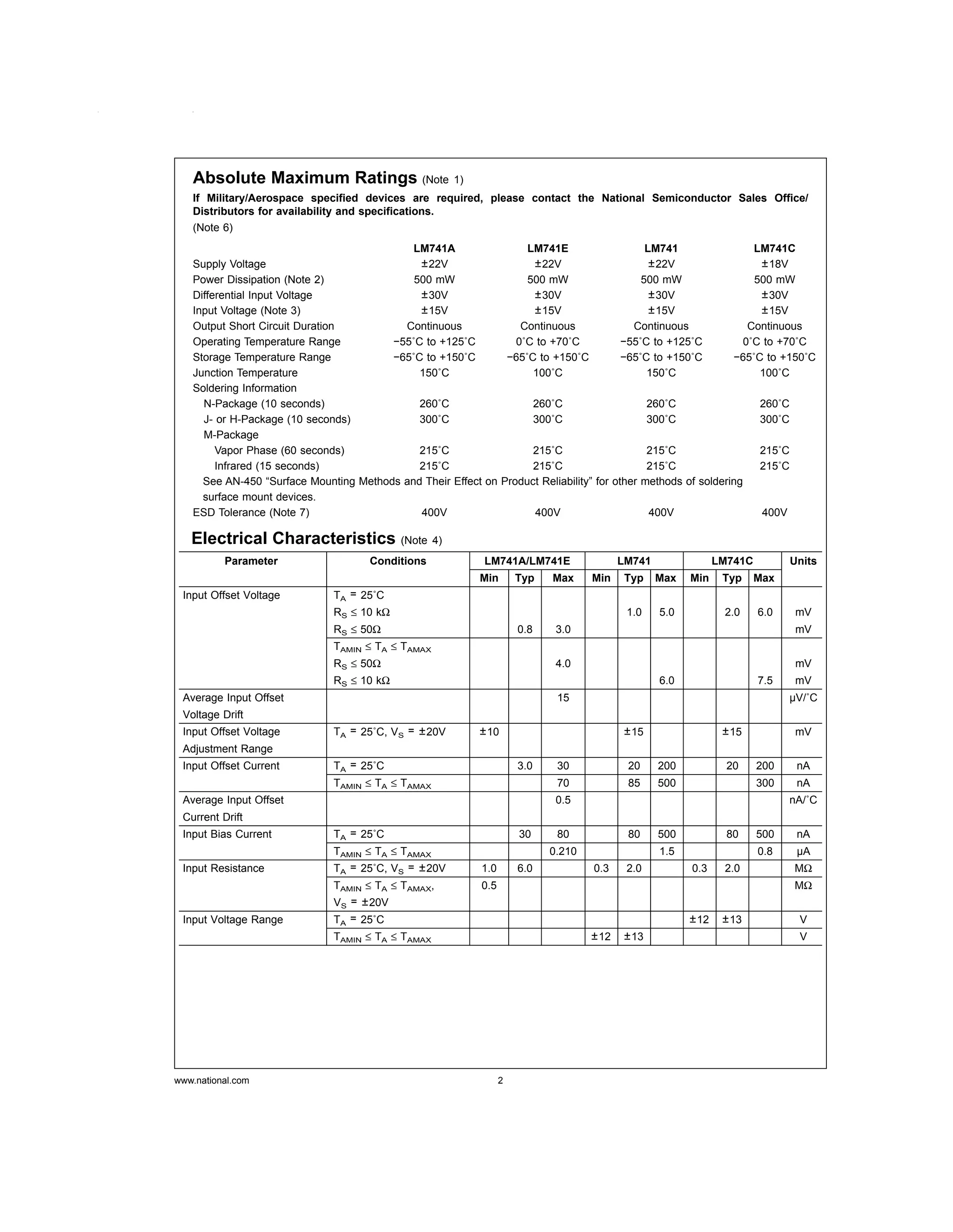


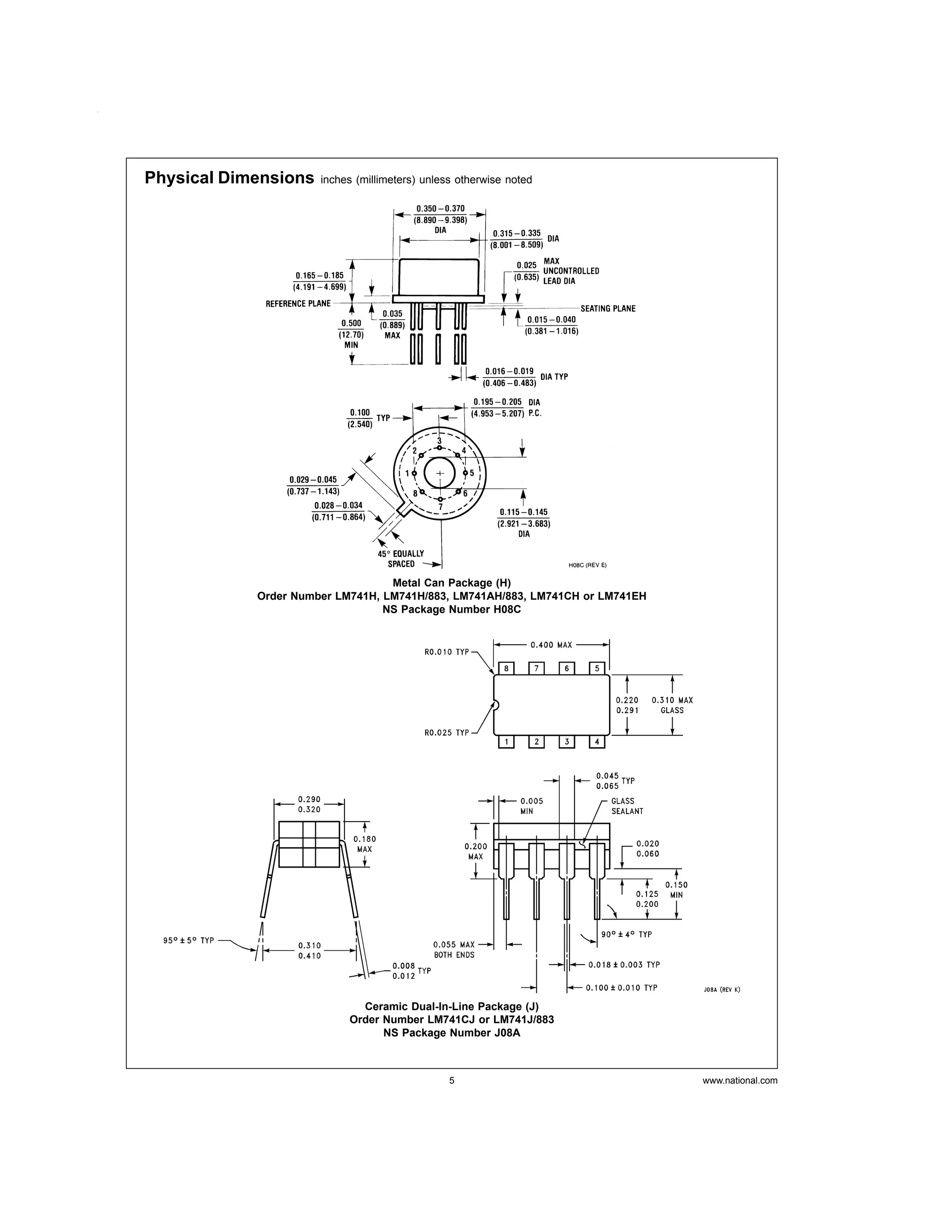

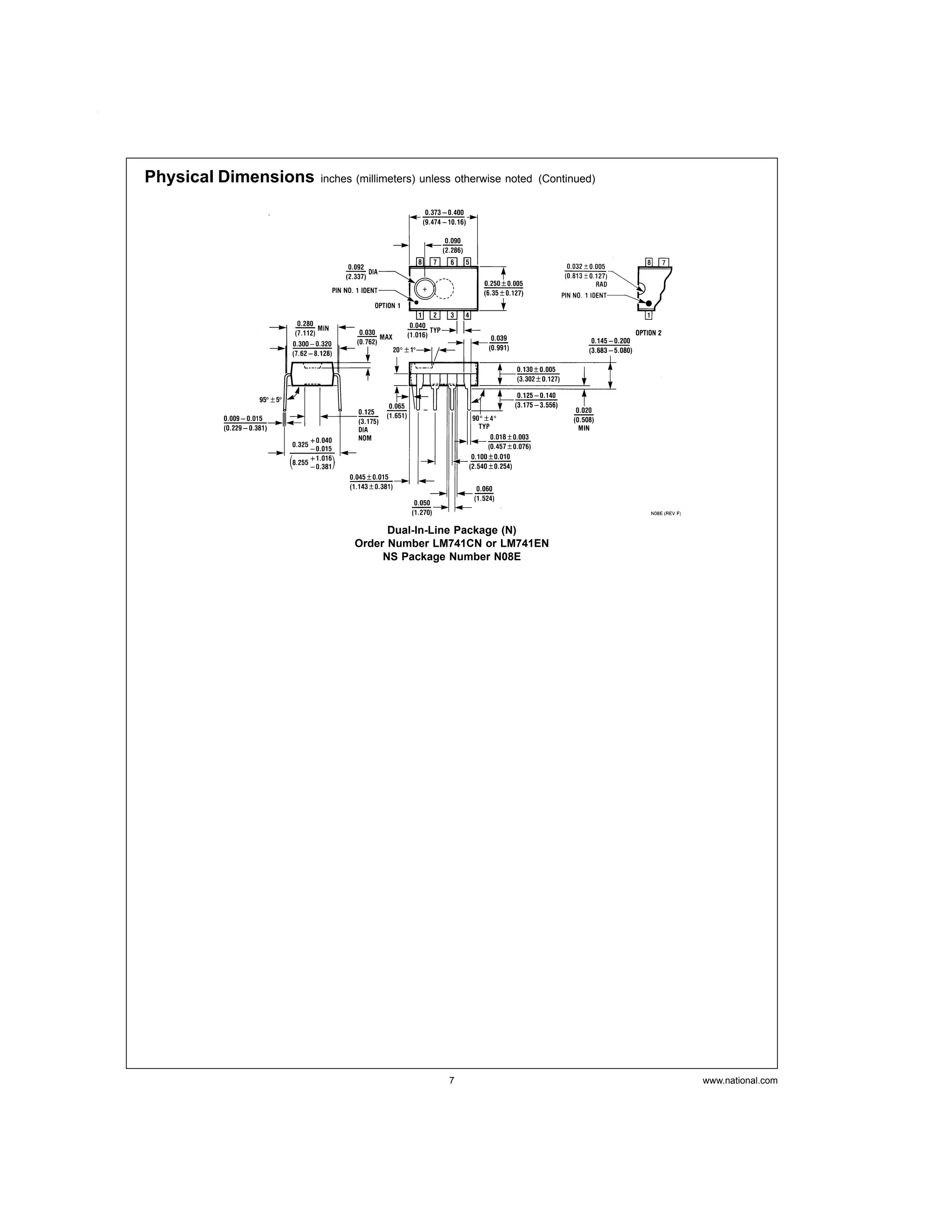

The document provides information about the LM741 operational amplifier, including: 1) It describes the LM741 as a general purpose operational amplifier that is a direct replacement for previous models and offers features like overload protection. 2) It provides the schematic diagram and pin connections for the LM741 in different package types. 3) It lists the electrical characteristics and specifications for the LM741 like voltage range, gain, bandwidth, power requirements, and packaging dimensions.


