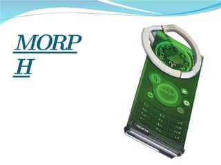
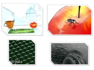
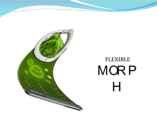
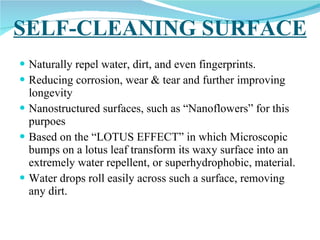
1. Morph is a concept phone developed by Nokia that utilizes nanotechnology to enable novel sensing, interface, and energy harvesting capabilities. It can detect chemicals, harvest solar energy through "nanowire grass", and has a self-cleaning surface.
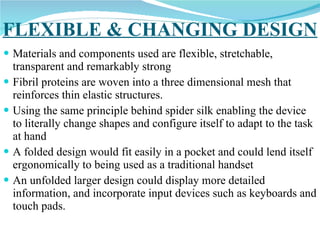
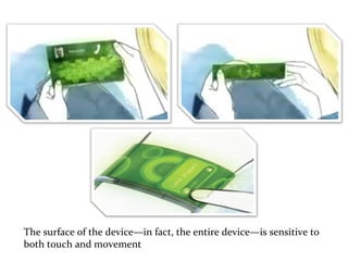
2. The device would be flexible, stretchable, and transparent using nanoscale electronics and biomimetic materials. Its entire surface would be a touch-sensitive interface.
3. Key challenges include ensuring a reliable power source and addressing health and environmental safety concerns around nanoparticle inhalation.