Downloaded 329 times


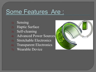
![2. HAPTIC SURFACE
Touch sensitive and responsive [haptic] surface of NOKIA morph is provided
by large area sensing surfaces using piezoelectric nanowire arrays.
ZnO nanowires are used to produce the piezoelectric nanowire arrays.
Buttons on the device surface are real 3D forms.](https://image.slidesharecdn.com/morphlatest-130927225646-phpapp01/85/Morph-latest-12-320.jpg)


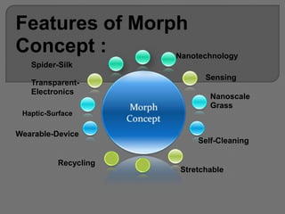
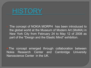
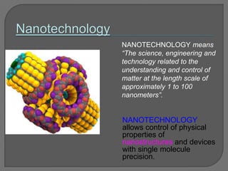
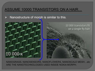
The document summarizes the theoretical Nokia Morph device concept which was presented at the Museum of Modern Art in 2008. The Morph concept demonstrates how future mobile devices could be stretchable, flexible, transparent and self-cleaning using nanotechnology. It would have sensing, haptic, self-cleaning and transparent display capabilities and use novel materials like nanograss, nanofibers and ZnO nanowires. However, the Morph would also face challenges like high initial costs, manufacturing difficulties, and material stability issues that must still be addressed.


